


CTLST CAT28F001TI-90TT, CAT28F001TI-90BT, CAT28F001TI-70TT, CAT28F001TI-70BT, CAT28F001TI-15TT Datasheet
...
|
|
|
|
|
|
CAT28F001 |
|
Licensed Intel |
1 Megabit CMOS Boot Block Flash Memory |
|
second source |
|
|
FEATURES
■Fast Read Access Time: 70/90/120/150 ns
■On-Chip Address and Data Latches
■Blocked Architecture
—One 8 KB Boot Block w/ Lock Out
•Top or Bottom Locations
—Two 4 KB Parameter Blocks
—One 112 KB Main Block
■Low Power CMOS Operation
■12.0V ± 5% Programming and Erase Voltage
■Automated Program & Erase Algorithms
■High Speed Programming
■Commercial, Industrial and Automotive Temperature Ranges
■Deep Powerdown Mode
—0.05 μA ICC Typical
—0.8 μA IPP Typical
■Hardware Data Protection
■Electronic Signature
■100,000 Program/Erase Cycles and 10 Year Data Retention
■JEDEC Standard Pinouts:
—32 pin DIP
—32 pin PLCC
—32 pin TSOP
■Reset/Deep Power Down Mode
DESCRIPTION
The CAT28F001 is a high speed 128K X 8 bit electrically erasable and reprogrammable Flash memory ideally suited for applications requiring in-system or after sale code updates.
The CAT28F001 has a blocked architecture with one 8 KB Boot Block, two 4 KB Parameter Blocks and one 112 KB Main Block. The Boot Block section can be at the top or bottom of the memory map and includes a reprogramming write lock out feature to guarantee data integrity. It is designed to contain secure code which will bring up the system minimally and download code to other locations of CAT28F001.
The CAT28F001 is designed with a signature mode which allows the user to identify the IC manufacturer and device type. The CAT28F001 is also designed with onChip Address Latches, Data Latches, Programming and Erase Algorithms.
The CAT28F001 is manufactured using Catalyst’s advanced CMOS floating gate technology. It is designed to endure 100,000 program/erase cycles and has a data retention of 10 years. The device is available in JEDEC approved 32-pin plastic DIP, PLCC or TSOP packages.
BLOCK DIAGRAM |
|
|
|
|
|
|
|
|
|
ADDRESS |
|
|
|
I/O0–I/O7 |
|
|
|
|
|
|
|
|
|
|
|
COUNTER |
|
|
|
|
|
|
|
|
|
|
|
I/O BUFFERS |
|
|
WRITE STATE |
|
ERASE VOLTAGE |
|
|
||
|
MACHINE |
|
|
SWITCH |
|
|
|
|
|
|
|
|
|
|
STATUS |
RP |
|
|
|
|
|
|
REGISTER |
WE |
COMMAND |
PROGRAM VOLTAGE |
CE, OE LOGIC |
DATA |
SENSE |
||
|
|||||||
|
REGISTER |
SWITCH |
|
LATCH |
AMP |
||
|
|
|
|||||
CE |
|
|
|
|
|
|
COMPARATOR |
OE |
|
|
|
|
|
|
|
|
|
LATCH |
|
|
|
Y-GATING |
|
|
|
|
|
|
|
||
|
|
ADDRESS |
Y-DECODER |
|
|
||
A0–A16 |
|
|
|
|
112K-BYTE MAIN BLOCK |
||
|
|
|
|
|
8K-BYTE BOOT BLOCK |
||
|
|
|
X-DECODER |
4K-BYTE PARAMETER BLOCK |
|||
|
VOLTAGE VERIFY |
|
4K-BYTE PARAMETER BLOCK |
||||
|
|
|
|
|
|
|
|
|
SWITCH |
|
|
|
|
|
|
|
|
|
|
|
|
|
28F001 F01 |
© 1998 by Catalyst Semiconductor, Inc. |
Doc. No. 25071-00 2/98 F-1 |
Characteristics subject to change without notice |
1 |
CAT28F001
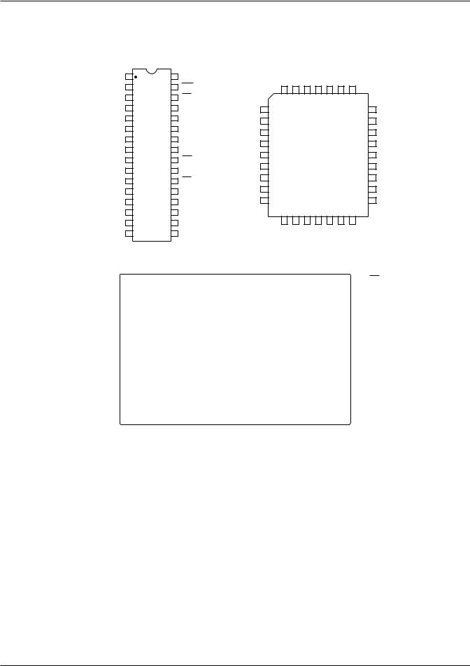
PIN CONFIGURATION
DIP Package (P)
VPP |
1 |
32 |
VCC |
A16 |
2 |
31 |
WE |
A15 |
3 |
30 |
RP |
A12 |
4 |
29 |
A14 |
A7 |
5 |
28 |
A13 |
A6 |
6 |
27 |
A8 |
A5 |
7 |
26 |
A9 |
A4 |
8 |
25 |
A11 |
A3 |
9 |
24 |
OE |
A2 |
10 |
23 |
A10 |
A1 |
11 |
22 |
CE |
A0 |
12 |
21 |
I/O7 |
I/O0 |
13 |
20 |
I/O6 |
I/O1 |
14 |
19 |
I/O5 |
I/O2 |
15 |
18 |
I/O4 |
VSS |
16 |
17 |
I/O3 |
PLCC Package (N)
|
12 |
15 |
16 |
PP |
CC |
|
WE |
|
RP |
|
|
|
|
|
|
|
|
|
|||||||
|
A |
A |
A |
V |
V |
|
|
|
|
|
||
|
4 |
3 |
2 |
1 |
32 31 30 |
|
|
|
||||
A7 |
5 |
|
|
|
|
|
|
29 |
A14 |
|||
A6 |
6 |
|
|
|
|
|
|
28 |
A13 |
|||
A5 |
7 |
|
|
|
|
|
|
27 |
A8 |
|||
A4 |
8 |
|
|
|
|
|
|
26 |
A9 |
|||
A3 |
9 |
|
|
|
|
|
|
25 |
A11 |
|||
A2 |
10 |
|
|
|
|
|
|
24 |
OE |
|
||
A1 |
11 |
|
|
|
|
|
|
23 |
A10 |
|||
A0 |
12 |
|
|
|
|
|
|
22 |
|
|
|
|
|
|
|
|
|
|
|
|
28F001 F02CE |
||||
I/O0 |
13 |
|
|
|
|
|
|
21 |
I/O7 |
|||
|
14 15 16 17 18 19 20 |
|
|
|
||||||||
|
1 |
2 |
SS |
3 |
4 |
5 |
6 |
|
|
|
||
|
I/O |
I/O |
V |
I/O |
I/O |
|
I/O |
|
I/O |
|
|
|
TSOP Package (Standard Pinout) (T)
A11 |
|
|
1 |
32 |
|
|
OE |
||||||
|
|
|
|
||||||||||
|
|
A9 |
|
2 |
31 |
|
|
A10 |
|||||
|
|
|
|||||||||||
|
|
A8 |
|
|
3 |
30 |
|
|
|
CE |
|
||
|
|
|
|
||||||||||
A13 |
|
4 |
29 |
|
|
I/O7 |
|||||||
|
|
|
|||||||||||
A14 |
|
5 |
28 |
|
|
I/O6 |
|||||||
|
|
|
|||||||||||
|
|
RP |
|
|
|
6 |
27 |
|
|
I/O5 |
|||
|
|
|
|||||||||||
|
WE |
|
|
|
7 |
26 |
|
|
I/O4 |
||||
|
|
|
|
||||||||||
VCC |
|
8 |
25 |
|
|
I/O3 |
|||||||
|
|
|
|||||||||||
VPP |
|
9 |
24 |
|
|
VSS |
|||||||
|
|
|
|||||||||||
A16 |
|
10 |
23 |
|
|
I/O2 |
|||||||
|
|
|
|||||||||||
A15 |
|
11 |
22 |
|
|
I/O1 |
|||||||
|
|
|
|||||||||||
A12 |
|
12 |
21 |
|
|
I/O0 |
|||||||
|
|
|
|||||||||||
|
|
A7 |
|
13 |
20 |
|
|
A0 |
|||||
|
|
|
|||||||||||
|
|
A6 |
|
14 |
19 |
|
|
A1 |
|||||
|
|
|
|||||||||||
|
|
A5 |
|
15 |
18 |
|
|
A2 |
|||||
|
|
|
|||||||||||
|
|
A4 |
|
16 |
17 |
|
|
A3 |
|||||
|
|
|
|||||||||||
PIN FUNCTIONS
Pin Name |
Type |
Function |
|
|||||||
|
|
|
|
|
|
|
|
|
|
|
|
A0–A16 |
Input |
Address Inputs for |
|
||||||
|
|
|
|
|
|
|
|
|
memory addressing |
|
|
|
|
|
|
|
|
|
|
|
|
|
I/O0–I/O7 |
I/O |
Data Input/Output |
|
||||||
|
|
|
|
|
|
|
|
|
|
|
|
|
|
|
|
|
|
Input |
Chip Enable |
|
|
|
CE |
|
|
|||||||
|
|
|
|
|
|
|
|
|
|
|
|
|
|
|
|
|
|
Input |
Output Enable |
|
|
|
OE |
|
||||||||
|
|
|
|
|
|
|
|
|
|
|
|
|
|
|
|
|
Input |
Write Enable |
|
||
|
WE |
|
||||||||
|
|
|
|
|
|
|
|
|
|
|
|
VCC |
|
Voltage Supply |
|
||||||
|
|
|
|
|
|
|
|
|
|
|
|
VSS |
|
Ground |
|
||||||
|
|
|
|
|
|
|
|
|
|
|
|
VPP |
|
Program/Erase |
|
||||||
|
|
|
|
|
|
|
|
|
Voltage Supply |
28F001 F03 |
|
|
|
|
|
|
|
|
|
|
|
|
|
|
|
Input |
Power Down |
|
||||
|
RP |
|
||||||||
|
|
|
|
|
|
|
|
|
|
|
Doc. No. 25071-00 2/98 F-1 |
2 |
|

CAT28F001
ABSOLUTE MAXIMUM RATINGS* |
*COMMENT |
Temperature Under Bias ................... |
–55°C to +95°C |
|
Storage Temperature ....................... |
–65°C to +150°C |
|
Voltage on Any Pin with |
|
|
Respect to Ground(1) ........... |
–2.0V to +VCC + 2.0V |
|
(Except A9, RP, OE, VCC and VPP) |
|
|
Voltage on Pin A9, RP AND OE with |
|
|
Respect to Ground(1) ................... |
–2.0V to +13.5V |
|
VPP with Respect to Ground |
|
|
during Program/Erase(1) .............. |
–2.0V to +14.0V |
|
VCC with Respect to Ground(1) ............ |
|
–2.0V to +7.0V |
Package Power Dissipation |
|
|
Capability (TA = 25°C) .................................. |
|
1.0 W |
Lead Soldering Temperature (10 secs) |
............ 300°C |
|
Output Short Circuit Current(2) ........................ |
|
100 mA |
RELIABILITY CHARACTERISTICS
Stresses above those listed under “Absolute Maximum Ratings” may cause permanent damage to the device. These are stress ratings only, and functional operation of the device at these or any other conditions outside of those listed in the operational sections of this specification is not implied. Exposure to any absolute maximum rating for extended periods may affect device performance and reliability.
Symbol |
Parameter |
Min. |
Max. |
Units |
Test Method |
|
|
|
|
|
|
NEND(3) |
Endurance |
100K |
|
Cycles/Byte |
MIL-STD-883, Test Method 1033 |
TDR(3) |
Data Retention |
10 |
|
Years |
MIL-STD-883, Test Method 1008 |
VZAP(3) |
ESD Susceptibility |
2000 |
|
Volts |
MIL-STD-883, Test Method 3015 |
ILTH(3)(4) |
Latch-Up |
100 |
|
mA |
JEDEC Standard 17 |
CAPACITANCE TA = 25°C, f = 1.0 MHz
|
|
|
Limits |
|
|
|
|
|
|
|
|
|
|
Symbol |
Test |
Min |
|
Max. |
Units |
Conditions |
|
|
|
|
|
|
|
CIN(3) |
Input Pin Capacitance |
|
|
8 |
pF |
VIN = 0V |
COUT(3) |
Output Pin Capacitance |
|
|
12 |
pF |
VOUT = 0V |
CVPP(3) |
VPP Supply Capacitance |
|
|
25 |
pF |
VPP = 0V |
Note:
(1)The minimum DC input voltage is –0.5V. During transitions, inputs may undershoot to –2.0V for periods of less than 20 ns. Maximum DC voltage on output pins is VCC +0.5V, which may overshoot to VCC + 2.0V for periods of less than 20ns.
(2)Output shorted for no more than one second. No more than one output shorted at a time.
(3)This parameter is tested initially and after a design or process change that affects the parameter.
(4)Latch-up protection is provided for stresses up to 100 mA on address and data pins from –1V to VCC +1V.
3 |
Doc. No. 25071-00 2/98 F-1 |

CAT28F001
D.C. OPERATING CHARACTERISTICS
VCC = +5V ±10%, unless otherwise specified
|
|
|
|
Limits |
|
|
|
|
|
|
|
|
|
|
|
|
|
|
|
|
|
|
|
|
|
|
|
|
|
|
|
|
|
|
|
|
|
|
|
|
|
Symbol |
Parameter |
Min. |
Max. |
Unit |
|
|
|
|
|
|
Test Conditions |
|||||||||
|
|
|
|
|
|
|
|
|
|
|
|
|
|
|
|
|
|
|
|
|
ILI |
Input Leakage Current |
|
|
±1.0 |
μA |
|
VIN = VCC or VSS |
|||||||||||||
|
|
|
|
|
|
|
VCC = 5.5V |
|||||||||||||
|
|
|
|
|
|
|
|
|
|
|
|
|
|
|
|
|
|
|
|
|
ILO |
Output Leakage Current |
|
|
±10 |
μA |
|
VOUT = VCC or VSS, |
|||||||||||||
|
|
|
|
|
|
|
VCC = 5.5V |
|||||||||||||
|
|
|
|
|
|
|
|
|
|
|
|
|
|
|
|
|
|
|
|
|
ISB1 |
VCC Standby Current CMOS |
|
|
100 |
μA |
|
|
|
= VCC ±0.2V = |
|
|
|
||||||||
|
|
|
CE |
RP |
|
|||||||||||||||
|
|
|
|
|
|
|
VCC = 5.5V |
|||||||||||||
ISB2 |
VCC Standby Current TTL |
|
|
1.5 |
mA |
|
|
|
|
|
= |
|
= VIH, VCC = 5.5V |
|||||||
|
|
|
|
CE |
RP |
|||||||||||||||
|
|
|
|
|
|
|
|
|
|
|
|
|
|
|
|
|
|
|
|
|
IPPD |
VPP Deep Powerdown Current |
|
|
1.0 |
μA |
|
|
|
|
|
|
= GND±0.2V |
||||||||
|
|
|
RP |
|||||||||||||||||
|
|
|
|
|
|
|
|
|
|
|
|
|
|
|
|
|
|
|
|
|
ICC1 |
VCC Active Read Current |
|
|
30 |
mA |
|
VCC = 5.5V, |
|
= VIL, |
|||||||||||
|
|
|
CE |
|||||||||||||||||
|
|
|
|
|
|
|
IOUT = 0mA, f = 8 MHz |
|||||||||||||
ICC2(1) |
VCC Programming Current |
|
|
20 |
mA |
|
VCC = 5.5V, |
|||||||||||||
|
|
|
|
|
|
|
Programming in Progress |
|||||||||||||
|
|
|
|
|
|
|
|
|
|
|
|
|
|
|
|
|
|
|
|
|
ICC3(1) |
VCC Erase Current |
|
|
20 |
mA |
|
VCC = 5.5V, |
|||||||||||||
|
|
|
|
|
|
|
Erase in Progress |
|||||||||||||
|
|
|
|
|
|
|
|
|
|
|
|
|
|
|
|
|
|
|
|
|
IPPS |
VPP Standby Current |
|
|
±10 |
μA |
|
VPP < VCC |
|||||||||||||
|
|
|
|
200 |
μA |
|
VPP > VCC |
|||||||||||||
|
|
|
|
|
|
|
|
|
|
|
|
|
|
|
|
|
|
|
|
|
IPP1 |
VPP Read Current |
|
|
200 |
μA |
|
VPP = VPPH |
|||||||||||||
|
|
|
|
|
|
|
|
|
|
|
|
|
|
|
|
|
|
|
|
|
IPP2(1) |
VPP Programming Current |
|
|
30 |
mA |
|
VPP = VPPH, |
|||||||||||||
|
|
|
|
|
|
|
Programming in Progress |
|||||||||||||
|
|
|
|
|
|
|
|
|
|
|
|
|
|
|
|
|
|
|
|
|
IPP3(1) |
VPP Erase Current |
|
|
30 |
mA |
|
VPP = VPPH, |
|||||||||||||
|
|
|
|
|
|
|
Erase in Progress |
|||||||||||||
|
|
|
|
|
|
|
|
|
|
|
|
|
|
|
|
|
|
|
|
|
VIL |
Input Low Level |
–0.5 |
0.8 |
V |
|
|
|
|
|
|
|
|
|
|
|
|
|
|
|
|
|
|
|
|
|
|
|
|
|
|
|
|
|
|
|
|
|
|
|
|
|
VOL |
Output Low Level |
|
|
0.45 |
V |
|
IOL = 5.8mA, VCC = 4.5V |
|||||||||||||
|
|
|
|
|
|
|
|
|
|
|
|
|
|
|
|
|
|
|
|
|
VIH |
Input High Level |
2.0 |
|
VCC+0.5 |
V |
|
|
|
|
|
|
|
|
|
|
|
|
|
|
|
VOH |
Output High Level |
2.4 |
|
|
V |
|
IOH = 2.5mA, VCC = 4.5V |
|||||||||||||
|
|
|
|
|
|
|
|
|
|
|
|
|
|
|
|
|
|
|
|
|
VID |
A9 Signature Voltage |
11.5 |
|
13.0 |
V |
|
A9 = VID |
|||||||||||||
|
|
|
|
|
|
|
|
|
|
|
|
|
|
|
|
|
|
|
|
|
IID |
A9 Signature Current |
|
|
500 |
μA |
|
A9 = VID |
|||||||||||||
ICCD |
VCC Deep Powerdown Current |
|
|
1.0 |
μA |
|
|
|
|
|
|
= GND±0.2V |
||||||||
|
|
|
RP |
|||||||||||||||||
|
|
|
|
|
|
|
|
|
|
|
|
|
|
|
|
|
|
|
|
|
ICCES |
VCC Erase Suspend Current |
|
|
10 |
mA |
|
Erase Suspended |
|
= VIH |
|||||||||||
|
|
CE |
||||||||||||||||||
|
|
|
|
|
|
|
|
|
|
|
|
|
|
|
|
|
|
|
|
|
IPPES |
VPP Erase Suspend Current |
|
|
300 |
μA |
|
Erase Suspended VPP=VPPH |
|||||||||||||
Note:
(1) This parameter is tested initially and after a design or process change that affects the parameter.
Doc. No. 25071-00 2/98 F-1 |
4 |
|
|
|
|
|
|
|
|
|
|
|
|
|
|
|
|
|
|
|
|
|
|
|
|
|
|
|
|
|
|
|
|
|
|
|
|
|
|
|
|
|
|
|
|
|
|
|
|
|
|
|
|
CAT28F001 |
|||
|
SUPPLY CHARACTERISTICS |
|
|
|
|
|
|
|
|
|
|
|
|
|
|
|
|
|
|
|
|
|
|
|
|
|
|
|||||||||||||||||||||||||||
|
|
|
|
|
|
|
|
|
|
|
|
|
|
|
|
|
|
|
|
|
|
|
|
|
|
|
|
|
|
|
|
|
|
|
|
|
|
|
|
|
|
|
|
|
|
|
|
|
|
|
|
|
||
|
|
|
|
|
|
|
|
|
|
|
|
|
|
|
|
|
|
|
|
|
|
|
|
|
|
|
|
|
|
|
|
|
|
|
Limits |
|
|
|
|
|
|
|
|
|
|
|
|
|
||||||
|
|
|
|
|
|
|
|
|
|
|
|
|
|
|
|
|
|
|
|
|
|
|
|
|
|
|
|
|
|
|
|
|
|
|
|
|
|
|
|
|
|
|
|
|
|
|
|
|
|
|
|
|
|
|
|
Symbol |
|
|
|
|
|
|
|
|
|
|
|
|
|
|
|
|
|
|
Parameter |
|
|
|
|
Min |
|
|
|
|
|
Max. |
|
|
|
|
|
Unit |
|
|
|||||||||||||||
|
|
|
|
|
|
|
|
|
|
|
|
|
|
|
|
|
|
|
|
|
|
|
|
|
|
|
|
|
|
|
|
|
|
|
|
|
|
|
|
|
|
|
|
|
|
|
|
|
|
|
|
|
|
|
|
VLKO |
|
|
|
|
|
|
|
|
|
VCC Erase/Write Lock Voltage |
|
|
|
|
2.5 |
|
|
|
|
|
|
|
|
|
|
|
|
|
|
|
|
|
V |
|
|
||||||||||||||||||
|
|
|
|
|
|
|
|
|
|
|
|
|
|
|
|
|
|
|
|
|
|
|
|
|
|
|
|
|
|
|
|
|
|
|
|
|
|
|
|
|
|
|
|
|
|
|
|
|
|
|
|
|
|
|
|
VCC |
|
|
|
|
|
|
|
|
|
VCC Supply Voltage |
|
|
|
|
4.5 |
|
|
|
|
|
|
|
5.5 |
|
|
|
|
|
|
V |
|
|
|||||||||||||||||||||
|
|
|
|
|
|
|
|
|
|
|
|
|
|
|
|
|
|
|
|
|
|
|
|
|
|
|
|
|
|
|
|
|
|
|
|
|
|
|
|
|
|
|
|
|
|
|
|
|
|
|
|
|
|
|
|
VPPL |
|
|
|
|
|
|
|
|
|
VPP During Read Operations |
|
|
|
|
0 |
|
|
|
|
|
|
|
6.5 |
|
|
|
|
|
|
V |
|
|
|||||||||||||||||||||
|
|
|
|
|
|
|
|
|
|
|
|
|
|
|
|
|
|
|
|
|
|
|
|
|
|
|
|
|
|
|
|
|
|
|
|
|
|
|
|
|
|
|
|
|
|
|
|
|
|
|
|
|
|
|
|
VPPH |
|
|
|
|
|
|
|
|
|
VPP During Erase/Program |
|
|
|
|
11.4 |
|
|
|
|
|
|
|
12.6 |
|
|
|
|
|
V |
|
|
||||||||||||||||||||||
|
|
|
|
|
|
|
|
|
|
|
|
|
|
|
|
|
|
|
|
|
|
|
|
|
|
|
|
|
|
|
|
|
|
|
|
|
|
|
|
|
|
|
|
|
|
|
|
|
|
|
|
|
|
|
|
VHH |
|
|
|
|
|
|
|
|
|
|
|
|
|
|
|
|
|
|
|
|
11.4 |
|
|
|
|
|
|
|
12.6 |
|
|
|
|
|
V |
|
|
||||||||||||||||
|
|
|
|
|
|
|
|
|
|
RP, OE Unlock Voltage |
|
|
|
|
|
|
|
|
|
|
|
|
|
|
|
|
|
|
||||||||||||||||||||||||||
|
|
|
|
|
|
|
|
|
|
|
|
|
|
|
|
|
|
|
|
|
|
|
|
|
|
|
|
|
|
|
|
|
|
|
|
|
|
|
|
|
|
|
|
|
|
|
|
|
|
|
|
|
|
|
|
A.C. CHARACTERISTICS, Read Operation |
|
|
|
|
|
|
|
|
|
|
|
|
|
|
|
|
|
|
|
|
|
|
|
|
|
|
|||||||||||||||||||||||||||
|
VCC = +5V ±10%, unless otherwise specified |
|
|
|
|
|
|
|
|
|
|
|
|
|
|
|
|
|
|
|
|
|
|
|
|
|
|
|||||||||||||||||||||||||||
|
JEDEC |
|
Standard |
|
|
|
|
|
|
|
|
|
|
|
|
|
|
|
|
|
|
|
28F001-70(8) |
28F001-90(7) |
|
|
28F001-12(7) |
|
|
28F001-15(7) |
|
|
||||||||||||||||||||||
|
Symbol |
|
Symbol |
|
|
|
|
|
|
|
|
|
|
|
Parameter |
|
Min. |
Max. |
Min. |
Max. |
|
|
Min. |
Max. |
|
Min. |
Max. |
Unit |
||||||||||||||||||||||||||
|
|
|
|
|
|
|
|
|
|
|
|
|
|
|
|
|
|
|
|
|
|
|
|
|
|
|
|
|
|
|
|
|
|
|
|
|
|
|
|
|
|
|
|
|
|
|
|
|
|
|||||
|
tAVAV |
|
tRC |
Read Cycle Time |
|
70 |
|
|
|
90 |
|
|
|
|
|
120 |
|
|
|
|
|
150 |
|
ns |
||||||||||||||||||||||||||||||
|
|
|
|
|
|
|
|
|
|
|
|
|
|
|
|
|
|
|
|
|
|
|
|
|
|
|
|
|
|
|
|
|
|
|
|
|
|
|
|
|
|
|
|
|
|
|
|
|
|
|
||||
|
tELQV |
|
tCE |
|
|
|
|
|
|
|
|
|
Access Time |
|
|
|
|
|
|
90 |
|
|
|
|
|
|
|
|
|
120 |
|
|
|
|
150 |
ns |
||||||||||||||||||
|
|
CE |
|
|
70 |
|
|
|
|
|
|
|
|
|
|
|
|
|
||||||||||||||||||||||||||||||||||||
|
|
|
|
|
|
|
|
|
|
|
|
|
|
|
|
|
|
|
|
|
|
|
|
|
|
|
|
|
|
|
|
|
|
|
|
|
|
|
|
|
|
|
|
|
|
|
|
|
|
|
||||
|
tAVQV |
|
tACC |
Address Access Time |
|
|
|
70 |
|
|
90 |
|
|
|
|
|
|
|
|
|
120 |
|
|
|
|
150 |
ns |
|||||||||||||||||||||||||||
|
|
|
|
|
|
|
|
|
|
|
|
|
|
|
|
|
|
|
|
|
|
|
|
|
|
|
|
|
|
|
|
|
|
|
|
|
|
|
|
|
|
|
|
|
|
|
|
|
|
|
||||
|
tGLQV |
|
tOE |
|
|
|
|
|
|
|
|
|
|
|
|
|
|
|
|
|
35 |
|
|
|
|
|
|
|
|
|
50 |
|
|
|
|
55 |
ns |
|||||||||||||||||
|
|
|
OE |
Access Time |
|
|
|
27 |
|
|
|
|
|
|
|
|
|
|
|
|
|
|
|
|
||||||||||||||||||||||||||||||
|
|
|
|
|
|
|
|
|
|
|
|
|
|
|
|
|
|
|
|
|
|
|
|
|
|
|
|
|
|
|
|
|
|
|
|
|
|
|
|
|
|
|
|
|
|
|
|
|
|
|
|
|||
|
- |
|
|
tOH |
|
|
|
|
|
|
|
|
|
|
|
|
|
|
|
|
|
|
|
|
|
|
|
|
|
|
|
|
|
|
|
|
|
|
|
|
|
|
|
|
|
|
|
|||||||
|
|
|
Output Hold from Address OE/CE |
Change |
|
0 |
|
|
|
0 |
|
|
|
|
|
|
|
0 |
|
|
|
|
|
|
0 |
|
ns |
|||||||||||||||||||||||||||
|
|
|
|
|
|
|
|
|
|
|
|
|
|
|
|
|
|
|
|
|
|
|
|
|
|
|
|
|
|
|
|
|
|
|
|
|
|
|
|
|
|
|
|
|
|
|
|
|
|
|
|
|||
|
tGLQX |
|
tOLZ(1)(6) |
|
|
|
|
|
|
to Output in Low-Z |
|
0 |
|
|
|
0 |
|
|
|
|
|
|
|
0 |
|
|
|
|
|
|
0 |
|
ns |
|||||||||||||||||||||
|
|
OE |
|
|
|
|
|
|
|
|
|
|
|
|
|
|
|
|
||||||||||||||||||||||||||||||||||||
|
tELQX |
|
tLZ(1)(6) |
|
|
|
|
|
|
|
|
|
0 |
|
|
|
0 |
|
|
|
|
|
|
|
0 |
|
|
|
|
|
|
0 |
|
ns |
||||||||||||||||||||
|
|
|
CE |
to Output in Low-Z |
|
|
|
|
|
|
|
|
|
|
|
|
|
|
|
|
||||||||||||||||||||||||||||||||||
|
tGHQZ |
|
tDF(1)(2) |
|
|
|
|
|
|
|
|
|
|
|
|
30 |
|
|
|
|
|
|
|
|
|
30 |
|
|
|
|
30 |
ns |
||||||||||||||||||||||
|
|
|
OE |
High to Output High-Z |
|
|
|
30 |
|
|
|
|
|
|
|
|
|
|
|
|
|
|
|
|
||||||||||||||||||||||||||||||
|
tEHQZ |
|
tHZ(1)(2) |
|
|
|
High to Output High-Z |
|
|
|
|
|
|
35 |
|
|
|
|
|
|
|
|
|
55 |
|
|
|
|
55 |
ns |
||||||||||||||||||||||||
|
|
CE |
|
|
55 |
|
|
|
|
|
|
|
|
|
|
|
|
|
||||||||||||||||||||||||||||||||||||
|
tPHQV |
|
tPWH |
|
|
|
|
|
600 |
|
|
600 |
|
|
|
|
|
|
|
600 |
|
|
|
|
600 |
ns |
||||||||||||||||||||||||||||
|
|
|
RP |
High to Output Delay |
|
|
|
|
|
|
|
|
|
|
|
|
|
|
|
|
|
|||||||||||||||||||||||||||||||||
|
|
|
|
|
|
|
|
|
|
|
|
|
|
|
|
|
|
|
|
|
|
|
|
|
|
|
|
|
|
|
|
|
|
|
|
|
|
|
|
|
|
|
|
|||||||||||
|
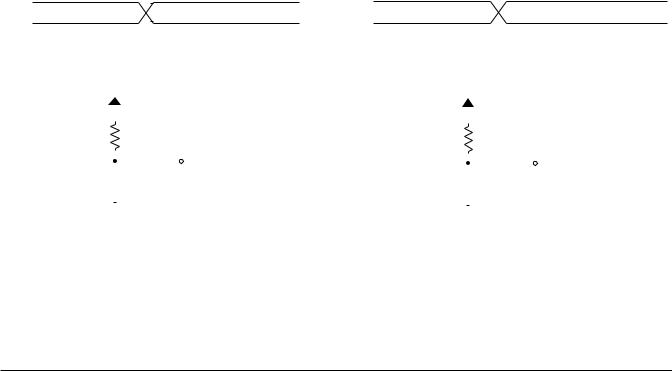
Figure 1. A.C. Testing Input/Output Waveform(3)(4)(5) |
Figure 2. Highspeed A.C. Testing Input/Output |
||||||||||||||||||||||||||||||||||||||||||||||||||||
|
|
|
|
|
|
|
|
|
|
|
|
|
|
|
|
|
|
|
|
|
|
|
|
|
|
|
|
|
|
|
|
|
Waveform(3)(4)(5) |
|
|
|
|
|
|
|
|
|||||||||||||
|
2.4 V |
|
|
|
|
|
|
|
|
|
|
|
|
|
|
|
|
2.0 V |
|
3.0 V |
|
|
|
|
|
|
|
|
|
|
|
|
|
|
|
|
|
|
|
|
|
|
||||||||||||
|
|
|
|
|
|
|
|
|
|
|
|
|
|
|
|
|
|
|
|
|
|
|
|
|
|
|
|
|
|
|
|
|
|
|
|
|
|
|
|
|
|
|
|
|
|
|||||||||
|
INPUT PULSE LEVELS |
|
|
|
|
|
|
|
|
|
|
|
|
|
REFERENCE POINTS |
|
|
|
INPUT PULSE LEVELS |
|
|
|
|
1.5 V |
|
|
REFERENCE POINTS |
|
|
|||||||||||||||||||||||||
|
|
|
|
|
|
|
|
|
|
|
|
|
|
|
|
|
|
|
|
|
|
|
|
|
||||||||||||||||||||||||||||||
|
0.45 V |
|
|
|
|
|
|
|
|
|
|
|
|
|
|
|
|
0.8 V |
|
0.0 V |
|
|
|
|
|
|
|
|
|
|
|
|
|
|
|
|
|
|
|
|
|
|
||||||||||||
|
|
|
|
|
|
|
|
|
|
|
|
|
|
|
|
|
|
|
|
|
|
|
|
|
|
|
|
|
|
|
|
|
|
|
|
|
|
|
|
|
|
|
|
|
|
|
|
|
||||||
|
|
|
|
|
|
|
|
|
|
|
|
|
|
|
|
|
|
|
|
|
|
|
|
5108 FHD F03 |
|
Testing Load Circuit (example) |
|
|
|
|
5108 FHD F03A |
|||||||||||||||||||||||
|
Testing Load Circuit (example) |
|
|
|
|
|
|
|
|
|||||||||||||||||||||||||||||||||||||||||||||
|
|
|
|
|
1.3V |
|
|
|
|
|
|
|
|
|
|
|
|
|
|
|
|
|
|
|
|
|
|
|
|
|
1.3V |
|
|
|
|
|
|
|
|
|
|
|
|
|
|
|
||||||||
|
|
|
|
|
|
|
|
|
|
1N914 |
|
|
|
|
|
|
|
|
|
|
|
1N914 |
|
|
|
|
|
|
|
|
||||||||||||||||||||||||
|
|
|
|
|
|
|
|
|
|
|
|
|
|
|
|
|
|
|
|
|
|
|
|
|
|
|
|
|
||||||||||||||||||||||||||
|
|
|
|
|
|
|
|
|
|
|
|
|
|
|
|
|
|
|
|
|
|
|
|
|
|
|
|
|
||||||||||||||||||||||||||
|
|
|
|
|
|
|
|
|
|
3.3K |
|
|
|
|
|
|
|
|
|
|
|
3.3K |
|
|
|
|
|
|
|
|
||||||||||||||||||||||||
|
DEVICE |
|
|
|
|
|
|
|
|
|
|
|
|
|
|
|
|
|
|
|
|
|
OUT |
|
|
DEVICE |
|
|
|
|
|
|
|
|
|
|
|
|
|
|
|
|
|
|
|
|
|
|
||||||
|
UNDER |
|
|
|
|
|
|
|
|
|
|
|
|
|
|
|
|
|
|
|
|
|
|
|
UNDER |
|
|
|
|
|
|
|
|
|
|
|
|
|
OUT |
|
|
|||||||||||||
|
|
|
|
|
|
|
|
|
|
|
|
|
|
|
|
|
|
|
|
|
|
|
|
|
|
|
|
|
|
|
|
|
|
|
|
|
|
|||||||||||||||||
|
|
|
|
|
|
|
|
|
|
|
|
|
|
|
|
|
|
|
|
|
|
|
|
|
|
|
|
|
|
|
|
|
|
|
|
|
|
|
|
|||||||||||||||
|
TEST |
|
|
|
|
|
|
|
CL = 100 pF |
|
|
|
TEST |
|
|
|
|
|
|
|
|
|
|
|
|
|
|
|
|
|
|
|
|
|
|
|||||||||||||||||||
|
|
|
|
|
|
|
|
|
|
|
|
|
|
|
|
|
|
|
|
|
C |
L |
= 30 pF |
|
|
|
|
|
|
|
|
|||||||||||||||||||||||
|
|
|
|
|
|
|
|
|
|
|
|
|
|
|
|
|
|
|
|
|
|
|
|
|
|
|
|
|
||||||||||||||||||||||||||
|
|
|
|
|
|
|
|
|
|
|
|
|
|
|
|
|
|
|
|
|
|
|
|
|
|
|
|
|
||||||||||||||||||||||||||
|
|
|
|
|
|
|
|
|
|
|
|
|
|
|
|
|
|
|
|
|
|
|
CL INCLUDES JIG CAPACITANCE |
|
|
|
|
|
|
|
|
|
|
|
|
|
|
|
|
|
C |
L |
INCLUDES JIG CAPACITANCE |
|||||||||||
|
|
|
|
|
|
|
|
|
|
|
|
|
|
|
|
|
|
|
|
|
|
|
|
|
|
|
|
|
|
|
|
|
|
|
|
|
|
|
||||||||||||||||
|
|
|
|
|
|
|
|
|
|
|
|
|
|
|
|
|
|
|
|
|
|
|
|
|
|
|
|
|
|
|
|
|
|
|
|
|
|
|
|
|||||||||||||||
|
|
|
|
|
|
|
|
|
|
|
|
|
|
|
|
|
|
|
|
|
|
|
|
|
5108 FHD F04 |
|
|
|
|
|
|
|
|
|
|
|
|
|
|
|
|
|
|
|
|
|
|
5108 FHD F05 |
||||||
|
|
|
|
|
|
|
|
|
|
|
|
|
|
|
|
|
|
|
|
|
|
|
|
|
|
|
|
|
|
|
|
|
|
|
|
|
|
|
|
|
|
|
|
|
|
|
|
|||||||
Note:
(1)This parameter is tested initially and after a design or process change that affects the parameter.
(2)Output floating (High-Z) is defined as the state where the external data line is no longer driven by the output buffer.
(3)Input Rise and Fall Times (10% to 90%) < 10 ns.
(4)Input Pulse Levels = 0.45V and 2.4V. For High Speed Input Pulse Levels 0.0V and 3.0V.
(5)Input and Output Timing Reference = 0.8V and 2.0V. For High Speed Input and Output Timing Reference = 1.5V.
(6)Low-Z is defined as the state where the external data may be driven by the output buffer but may not be valid.
(7)For load and reference points, see Fig. 1
(8)For load and reference points, see Fig. 2
5 |
Doc. No. 25071-00 2/98 F-1 |

CAT28F001
A.C. CHARACTERISTICS, Program/Erase Operation
VCC = +5V ±10%
JEDEC |
Standard |
|
|
|
|
|
|
|
|
|
|
|
|
|
|
|
|
|
|
|
|
|
28F001-70 |
28F001-90 |
28F001-12 |
28F001-15 |
|
||||
|
|
|
|
|
|
|
|
|
|
|
|
|
|
|
|
|
|
|
|
|
|
|
|
|
|
|
|
|
|
|
|
Symbol |
Symbol |
|
Parameter |
Min. |
Max. |
Min. |
Max. |
Min. |
Max. |
Min. |
Max. |
Unit |
|||||||||||||||||||
|
|
|
|
|
|
|
|
|
|
|
|
|
|
|
|
|
|
|
|
|
|
|
|
|
|
|
|
|
|
|
|
tAVAV |
tWC |
|
Write Cycle Time |
70 |
|
90 |
|
120 |
|
150 |
|
ns |
|||||||||||||||||||
|
|
|
|
|
|
|
|
|
|
|
|
|
|
|
|
|
|
|
|
|
|
|
|
|
|
|
|
|
|
|
|
|
|
|
|
|
|
|
|
|
|
|
|
|
|
|
|
|
|
|
|
|
|
|
|
|
|
|
|||||
tAVWH |
tAS |
|
Address Setup to WE Going High |
35 |
|
40 |
|
40 |
|
40 |
|
ns |
|||||||||||||||||||
|
|
|
|
|
|
|
|
|
|
|
|
|
|
|
|
|
|
|
|
|
|
|
|
|
|
|
|
|
|
|
|
|
|
|
|
|
|
|
|
|
|
|
|
|
|
|
|
|
|
|
|
|
|
|
|
|
|
|
|
|
|
|
|
tWHAX |
tAH |
|
Address Hold Time from WE Going High |
10 |
|
10 |
|
10 |
|
10 |
|
ns |
|||||||||||||||||||
|
|
|
|
|
|
|
|
|
|
|
|
|
|
|
|
|
|
|
|
|
|
|
|
|
|
|
|
|
|
|
|
|
|
|
|
|
|
|
|
|
|
|
|
|
|
|
|
|
|
|
|
|
|
|
|
|
|
||||||
tDVWH |
tDS |
|
Data Setup Time to WE Going High |
35 |
|
40 |
|
40 |
|
40 |
|
ns |
|||||||||||||||||||
|
|
|
|
|
|
|
|
|
|
|
|
|
|
|
|
|
|
|
|
|
|
|
|
|
|
|
|
|
|
|
|
|
|
|
|
|
|
|
|
|
|
|
|
|
|
|
|
10 |
|
|
|
|
|
|
|
|
|||||||
tWHDX |
tDH |
|
Data Hold Time from |
WE |
|
Going High |
|
10 |
|
10 |
|
10 |
|
ns |
|||||||||||||||||
|
|
|
|
|
|
|
|
|
|
|
|
|
|
|
|
|
|
|
|
|
|
|
|
|
|
|
|
|
|
|
|
tELWL |
tCS |
|
|
|
|
|
|
|
|
|
|
|
|
0 |
|
0 |
|
0 |
|
0 |
|
ns |
|||||||||
|
CE |
Setup Time to |
WE |
Going Low |
|
|
|
|
|||||||||||||||||||||||
|
|
|
|
|
|
|
|
|
|
|
|
|
|
|
|
|
|
|
|
|
|
|
|
|
|
|
|
|
|
|
|
|
|
|
|
|
|
|
|
|
|
|
|
|
|
0 |
|
|
|
|
|
|
|
|
|||||||||
tWHEH |
tCH |
|
CE |
|
Hold Time from WE Going High |
|
0 |
|
0 |
|
0 |
|
ns |
||||||||||||||||||
|
|
|
|
|
|
|
|
|
|
|
|
|
|
|
|
|
|
|
|
|
|
|
|
|
|
|
|
|
|
|
|
|
|
|
|
|
|
|
|
|
|
|
35 |
|
|
|
|
|
|
|
|
||||||||||||
tWLWH |
tWP |
|
WE Pulse Width |
|
40 |
|
40 |
|
40 |
|
ns |
||||||||||||||||||||
|
|
|
|
|
|
|
|
|
|
|
|
|
|
|
|
|
|
|
|
|
|
|
|
|
|
|
|
|
|
|
|
|
|
|
|
|
|
|
|
|
|
|
10 |
|
|
|
|
|
|
|
|
||||||||||||
tWHWL |
tWPH |
|
WE High Pulse Width |
|
10 |
|
10 |
|
10 |
|
ns |
||||||||||||||||||||
|
|
|
|
|
|
|
|
|
|
|
|
|
|
|
|
|
|
|
|
|
|
|
|
|
|
|
|
|
|
|
|
tWHGL |
— |
|
Write Recovery Time Before Read |
0 |
|
0 |
|
0 |
|
0 |
|
μs |
|||||||||||||||||||
|
|
|
|
|
|
|
|
|
|
|
|
|
|
|
|
|
|
|
|
|
|
|
|
|
|
|
|
|
|
|
|
|
tPS(1) |
|
|
|
|
|
|
|
480 |
|
|
|
|
|
|
|
|
||||||||||||||
tPHWL |
|
RP High Recovery to WE Going Low |
|
480 |
|
480 |
|
480 |
|
ns |
|||||||||||||||||||||
|
tPHS(1) |
|
|
|
|
|
|
|
|
100 |
|
|
|
|
|
|
|
|
|||||||||||||
tPHHWH |
|
RP VHH Setup to WE Going High |
|
100 |
|
100 |
|
100 |
|
ns |
|||||||||||||||||||||
|
tVPS(1) |
|
|
|
|
100 |
|
|
|
|
|
|
|
|
|||||||||||||||||
tVPWH |
|
VPP Setup to WE Going High |
|
100 |
|
100 |
|
100 |
|
ns |
|||||||||||||||||||||
tWHQV1 |
— |
|
Duration of Programming Operations |
15 |
|
15 |
|
15 |
|
15 |
|
μs |
|||||||||||||||||||
|
|
|
|
|
|
|
|
|
|
|
|
|
|
|
|
|
|
|
|
|
|
|
|
|
|
|
|
|
|
|
|
tWHQV2 |
— |
|
Duration of Erase Operations (Boot) |
1.3 |
|
1.3 |
|
1.3 |
|
1.3 |
|
Sec |
|||||||||||||||||||
|
|
|
|
|
|
|
|
|
|
|
|
|
|
|
|
|
|
|
|
|
|
|
|
|
|
|
|
|
|
|
|
tWHQV3 |
— |
|
Duration of Erase Operations (Parameter) |
1.3 |
|
1.3 |
|
1.3 |
|
1.3 |
|
Sec |
|||||||||||||||||||
|
|
|
|
|
|
|
|
|
|
|
|
|
|
|
|
|
|
|
|
|
|
|
|
|
|
|
|
|
|
|
|
tWHQV4 |
— |
|
Duration of Erase Operations (Main) |
3 |
|
3 |
|
3 |
|
3 |
|
Sec |
|||||||||||||||||||
|
|
|
|
|
|
|
|
|
|
|
|
|
|
|
|
|
|
|
|
|
|
|
|
|
|
|
|
|
|
|
|
tQVVL |
tVPH(1) |
|
VPP Hold from Valid Status Reg Data |
0 |
|
0 |
|
0 |
|
0 |
|
ns |
|||||||||||||||||||
|
tPHH(1) |
|
|
|
|
|
|
|
|
|
|
|
|
|
|
|
|
|
|
|
|
|
|
|
|||||||
tQVPH |
|
RP VHH Hold from Status Reg Data |
0 |
|
0 |
|
0 |
|
0 |
|
ns |
||||||||||||||||||||
tPHBR(1) |
— |
|
Boot Block Relock Delay |
|
100 |
|
100 |
|
100 |
|
100 |
ns |
|||||||||||||||||||
|
|
|
|
|
|
|
|
|
|
|
|
|
|
|
|
|
|
|
|
|
|
|
|
|
|
|
|
|
|
||
tGHHWL |
— |
|
OE VHH Setup to WE Going Low |
480 |
|
480 |
|
480 |
|
480 |
|
ns |
|||||||||||||||||||
|
|
|
|
|
|
|
|
|
|
|
|
|
|
|
|
|
|
|
|
|
|
|
|
|
|
|
|
|
|
|
|
|
|
|
|
|
|
|
|
|
|
|
|
|
|
|
|
|
|
|
|
|
|
|
|
|
|
|
|
|
|
||
tWHGH |
— |
|
OE VHH Hold from WE High |
480 |
|
480 |
|
480 |
|
480 |
|
ns |
|||||||||||||||||||
|
|
|
|
|
|
|
|
|
|
|
|
|
|
|
|
|
|
|
|
|
|
|
|
|
|
|
|
|
|
|
|
Note:
(1) This parameter is tested initially and after a design or process change that affects the parameter.
Doc. No. 25071-00 2/98 F-1 |
6 |
|
 Loading...