


CTLST CAT28C513N-12T, CAT28C513HNI-15T, CAT28C513HNA-15T, CAT28C513HNA-12T, CAT28C513HN-15T Datasheet
...
Advanced
CAT28C512/513
512K-Bit CMOS PARALLEL E2PROM
FEATURES
■Fast Read Access Times: 120/150 ns
■Low Power CMOS Dissipation:
–Active: 50 mA Max. –Standby: 200μA Max.
■Simple Write Operation:
–On-Chip Address and Data Latches –Self-Timed Write Cycle with Auto-Clear
■Fast Write Cycle Time: –5ms Max
■CMOS and TTL Compatible I/O
■Automatic Page Write Operation: –1 to 128 Bytes in 5ms
–Page Load Timer
■End of Write Detection: –Toggle Bit
–DATA Polling
■Hardware and Software Write Protection
■100,000 Program/Erase Cycles
■100 Year Data Retention
■Commercial, Industrial and Automotive Temperature Ranges
DESCRIPTION
The CAT28C512/513 is a fast,low power, 5V-only CMOS parallel E2PROM organized as 64K x 8-bits. It requires a simple interface for in-system programming. On-chip address and data latches, self-timed write cycle with auto-clear and VCC power up/down write protection eliminate additional timing and protection hardware. DATA Polling and Toggle status bits signal the start and end of the self-timed write cycle. Additionally, the CAT28C512/513 features hardware and software write protection.
The CAT28C512/513 is manufactured using Catalyst’s advanced CMOS floating gate technology. It is designed to endure 100,000 program/erase cycles and has a data retention of 100 years. The device is available in JEDEC approved 32-pin DIP, PLCC, 32-pin TSOP and 40-pin TSOP packages.
BLOCK DIAGRAM |
|
|
|
|
A7–A15 |
ADDR. BUFFER |
ROW |
65,536 x 8 |
|
& LATCHES |
DECODER |
E2PROM |
||
|
|
|
ARRAY |
|
VCC |
INADVERTENT |
HIGH VOLTAGE |
128 BYTE PAGE |
|
WRITE |
GENERATOR |
|||
REGISTER |
||||
|
PROTECTION |
|
||
|
|
|
||
CE |
CONTROL |
|
|
|
OE |
|
|
||
WE |
|
|
I/O BUFFERS |
|
|
|
|
||
|
|
DATA POLLING |
|
|
|
TIMER |
AND |
|
|
|
|
TOGGLE BIT |
I/O0–I/O7 |
|
|
|
|
||
A0–A6 |
ADDR. BUFFER |
COLUMN |
|
|
& LATCHES |
|
|||
|
DECODER |
|
||
|
|
|
||
|
|
|
5096 FHD F02 |
© 1998 by Catalyst Semiconductor, Inc. |
1 |
Doc. No. 25074-00 2/98 |
Characteristics subject to change without notice |
|
CAT28C512/513 Advanced
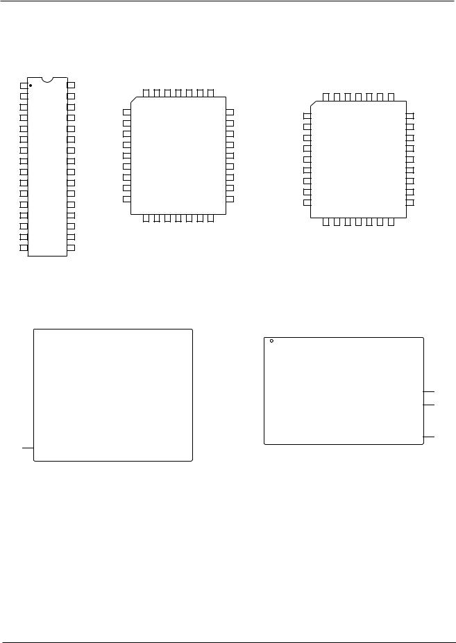
PIN CONFIGURATION
|
|
DIP Package (P) |
|
PLCC Package (N) |
|
|
PLCC Package (N) |
|
|||||||||||||||
NC |
1 |
32 |
VCC |
|
12 |
15 |
NC |
NC |
CC |
WE |
NC |
|
|
7 |
12 |
14 |
15 |
CC |
WE |
13 |
|
||
|
A |
A |
V |
|
|
A |
A |
A |
A |
V |
A |
|
|||||||||||
NC |
2 |
31 |
WE |
|
4 |
3 |
2 |
1 |
32 31 30 |
|
|
|
|
|
|
|
|
|
|
||||
A15 |
3 |
30 |
NC |
A7 |
A14 |
|
4 |
3 |
2 |
1 |
32 31 30 |
|
|||||||||||
5 |
|
|
|
|
|
29 |
A6 |
A8 |
|||||||||||||||
A12 |
4 |
29 |
A14 |
A6 |
6 |
|
|
|
|
|
28 |
A13 |
5 |
|
|
|
|
|
29 |
||||
A |
7 |
5 |
28 |
A |
13 |
|
|
|
|
|
A5 |
6 |
|
|
|
|
|
28 |
A9 |
||||
A5 |
7 |
|
|
|
|
|
27 |
A8 |
|
|
|
|
|
||||||||||
A |
6 |
27 |
A |
|
|
|
|
|
A4 |
7 |
|
|
|
|
|
27 |
A11 |
||||||
6 |
8 |
A4 |
8 |
|
|
|
|
|
26 |
A9 |
|
|
|
|
|
||||||||
|
7 |
26 |
|
CAT28C512 |
A3 |
8 |
CAT28C513 |
26 |
NC |
||||||||||||||
A5 |
A9 |
A3 |
9 |
25 |
|
||||||||||||||||||
A4 |
8 |
25 |
A11 |
TOP VIEW |
|
A11 |
A2 |
9 |
TOP VIEW |
|
25 |
OE |
|||||||||||
A2 |
10 |
|
|
|
|
|
24 |
OE |
A1 |
10 |
|
|
|
|
|
24 |
A10 |
||||||
A3 |
9 |
24 |
OE |
A1 |
11 |
|
|
|
|
|
23 |
A10 |
|
|
|
|
|
||||||
A2 |
10 |
23 |
A10 |
|
|
|
|
|
A0 |
11 |
|
|
|
|
|
23 |
CE |
||||||
A0 |
12 |
|
|
|
|
|
22 |
CE |
|
12 |
|
|
|
|
|
22 |
|||||||
A1 |
11 |
22 |
CE |
I/O0 |
13 |
|
|
|
|
|
21 |
|
NC |
|
|
|
|
|
I/O7 |
||||
|
|
|
|
|
I/O7 |
13 |
|
|
|
|
|
21 |
|||||||||||
A0 |
12 |
21 |
I/O7 |
|
|
|
|
|
I/O0 |
|
|
|
|
|
I/O6 |
||||||||
|
14 15 16 17 18 19 20 |
|
14 15 16 17 18 19 20 |
||||||||||||||||||||
I/O0 |
13 |
20 |
I/O6 |
|
|
|
|
|
|
|
|
|
|
|
|||||||||
|
|
|
|
|
|
|
|
|
|
|
|
|
|
|
|
|
|
||||||
I/O1 |
14 |
19 |
I/O5 |
|
1 |
2 |
SS |
3 |
4 |
5 |
6 |
|
|
1 |
2 |
SS |
NC |
3 |
4 |
5 |
|
||
I/O2 |
15 |
18 |
I/O4 |
|
|
|
|
||||||||||||||||
|
I/O |
I/O |
V |
I/O |
I/O |
I/O |
I/O |
|
|
I/O |
I/O |
V |
I/O |
I/O |
I/O |
|
|||||||
VSS |
16 |
17 |
I/O3 |
|
|
|
|
|
|
|
|
5096 FHD F01 |
|
|
|
|
|
|
|
|
|
||
TSOP Package (10mm X 14mm) (T14) |
TSOP Package (8mmx20mm) (T) |
A11 

 1
1 
A9  2
2
A8 

 3
3
A13 

 4 A14
4 A14 

 5 NC
5 NC 

 6 NC
6 NC 

 7 NC
7 NC 

 8
8
WE  9
9
VCC 

 10 NC
10 NC 

 11
11
NC 

 12 NC
12 NC 

 13 NC
13 NC 

 14 A15

 15 A12

 16
16
A7  17 A6
17 A6  18 A5
18 A5  19 A4
19 A4 

 20
20
CAT28C512
TOP VIEW
40 |
|
|
|
|
|
|
OE |
|
|
|
|
|
|
|
|
|
|
|
|
|
|
|
|
|
|||
39 |
|
|
|
|
|
|
A10 |
A11 |
|
|
|
1 |
|
38 |
|
|
|
|
|
|
CE |
|
|
|
|||
37 |
|
|
|
|
|
|
I/O7 |
A9 |
|
|
|
2 |
|
36 |
|
|
|
|
|
|
I/O6 |
A8 |
|
|
|
3 |
|
|
|
|
|
|
|
|
A13 |
|
|
|
4 |
||
35 |
|
|
|
|
|
|
I/O5 |
A14 |
|
|
|
5 |
|
|
|
|
|
|
|
|
|
|
|
||||
34 |
|
|
|
|
|
|
I/O4 |
NC |
|
|
|
6 |
|
33 |
|
|
|
|
|
|
I/O3 |
|
|
|
7 |
||
32 |
|
|
|
|
|
|
WE |
|
|
|
|||
|
|
|
|
|
|
NC |
VCC |
|
|
|
8 |
||
31 |
|
|
|
|
|
|
NC |
|
|
|
|||
30 |
|
|
|
|
|
|
VSS |
NC |
|
|
|
9 |
|
29 |
|
|
|
|
|
|
NC |
|
|
|
10 |
||
28 |
|
|
|
|
|
|
NC |
A15 |
|
|
|
11 |
|
|
|
|
|
|
|
NC |
|
|
|
||||
27 |
|
|
|
|
|
|
I/O2 |
A12 |
|
|
|
12 |
|
26 |
|
|
|
|
|
|
A7 |
|
|
|
13 |
||
25 |
|
|
|
|
|
|
I/O1 |
A6 |
|
|
|
14 |
|
|
|
|
|
|
|
|
I/O0 |
A5 |
|
|
|
15 |
|
|
|
|
|
|
|
|
|
|
|
||||
24 |
|
|
|
|
|
|
A0 |
|
|
|
|
|
16 |
23 |
|
|
|
|
|
|
A1 |
A4 |
|
||||
|
|
|
|
|
|
|
|
||||||
22 |
|
|
|
|
|
|
A2 |
|
|
|
|
|
|
|
|
|
|
|
|
|
|
|
|
|
|
||
21 |
|
|
|
|
|
|
A3 |
|
|
|
|
|
|
|
|
|
|
|
|
|
|
|
|
|
|
||
CAT28C512
TOP VIEW
32 

 OE
OE
31  A10
A10
30 

 CE
CE
29 

 I/O7
I/O7
28  I/O6
I/O6
27  I/O5
I/O5
26  I/O4
I/O4
25  I/O3
I/O3
24 

 Vss
Vss
23 

 I/O2
I/O2
22  I/O1
I/O1
21 

 I/O0
I/O0
20  A0
A0
19 

 A1
A1
18  A2
A2
17 

 A3
A3
PIN FUNCTIONS
Pin Name |
Function |
Pin Name |
Function |
|
|
|
|
A0–A15 |
Address Inputs |
WE |
Write Enable |
|
|
|
|
I/O0–I/O7 |
Data Inputs/Outputs |
VCC |
5V Supply |
|
|
|
|
CE |
Chip Enable |
VSS |
Ground |
|
|
|
|
OE |
Output Enable |
NC |
No Connect |
|
|
|
|
Doc. No. 25074-00 2/98 |
2 |
|

Advanced |
CAT28C512/513 |
ABSOLUTE MAXIMUM RATINGS* |
*COMMENT |
Temperature Under Bias ................. |
–55°C to +125°C |
|
Storage Temperature ....................... |
–65°C to +150°C |
|
Voltage on Any Pin with |
|
|
Respect to Ground(2) ........... |
–2.0V to +VCC + 2.0V |
|
VCC with Respect to Ground ............... |
|
–2.0V to +7.0V |
Package Power Dissipation |
|
|
Capability (Ta = 25°C) ................................... |
|
1.0W |
Lead Soldering Temperature (10 secs) |
............ 300°C |
|
Output Short Circuit Current(3) ........................ |
|
100 mA |
RELIABILITY CHARACTERISTICS
Stresses above those listed under “Absolute Maximum Ratings” may cause permanent damage to the device. These are stress ratings only, and functional operation of the device at these or any other conditions outside of those listed in the operational sections of this specification is not implied. Exposure to any absolute maximum rating for extended periods may affect device performance and reliability.
Symbol |
Parameter |
Min. |
Max. |
Units |
Test Method |
|
|
|
|
|
|
NEND(1) |
Endurance |
104 or 105 |
|
Cycles/Byte |
MIL-STD-883, Test Method 1033 |
TDR(1) |
Data Retention |
100 |
|
Years |
MIL-STD-883, Test Method 1008 |
VZAP(1) |
ESD Susceptibility |
2000 |
|
Volts |
MIL-STD-883, Test Method 3015 |
ILTH(1)(4) |
Latch-Up |
100 |
|
mA |
JEDEC Standard 17 |
D.C. OPERATING CHARACTERISTICS
VCC = 5V ±10%, unless otherwise specified.
|
|
|
Limits |
|
|
|
|
|
|
|
|
|
|
Symbol |
Parameter |
Min. |
Typ. |
Max. |
Units |
Test Conditions |
|
|
|
|
|
|
|
ICC |
VCC Current (Operating, TTL) |
|
|
50 |
mA |
CE = OE = VIL, f=6MHz |
|
|
|
|
|
|
All I/O’s Open |
|
|
|
|
|
|
|
ICCC(5) |
VCC Current (Operating, CMOS) |
|
|
25 |
mA |
CE = OE = VILC, f=6MHz |
|
|
|
|
|
|
All I/O’s Open |
|
|
|
|
|
|
|
ISB |
VCC Current (Standby, TTL) |
|
|
3 |
mA |
CE = VIH, All I/O’s Open |
ISBC(6) |
VCC Current (Standby, CMOS) |
|
|
200 |
μA |
CE = VIHC, |
|
|
|
|
|
|
All I/O’s Open |
|
|
|
|
|
|
|
ILI |
Input Leakage Current |
-10 |
|
10 |
μA |
VIN = GND to VCC |
ILO |
Output Leakage Current |
-10 |
|
10 |
μA |
VOUT = GND to VCC, |
|
|
|
|
|
|
CE = VIH |
VIH(6) |
High Level Input Voltage |
2 |
|
VCC +0.3 |
V |
|
VIL(5) |
Low Level Input Voltage |
-1 |
|
0.8 |
V |
|
VOH |
High Level Output Voltage |
2.4 |
|
|
V |
IOH = –400μA |
VOL |
Low Level Output Voltage |
|
|
0.4 |
V |
IOL = 2.1mA |
VWI |
Write Inhibit Voltage |
3.5 |
|
|
V |
|
|
|
|
|
|
|
|
Note:
(1)This parameter is tested initially and after a design or process change that affects the parameter.
(2)The minimum DC input voltage is –0.5V. During transitions, inputs may undershoot to –2.0V for periods of less than 20 ns. Maximum DC voltage on output pins is VCC +0.5V, which may overshoot to VCC +2.0V for periods of less than 20 ns.
(3)Output shorted for no more than one second. No more than one output shorted at a time.
(4)Latch-up protection is provided for stresses up to 100mA on address and data pins from –1V to VCC +1V.
(5)VILC = –0.3V to +0.3V.
(6)VIHC = VCC –0.3V to VCC +0.3V.
3 |
Doc. No. 25074-00 2/98 |
|
 Loading...