


Do not disconnect modules when they are energized!
Repairs on power supply section are to be carried out only with isolating transformer.
Ne pas retirer les modules lorsqu' ils sont sous tension. N'effectuer les travaux de maintenance sur la partie reliée au secteur (Switch Mode) qu'au travers d'un transformateur d'isolement.
Module nicht bei eingeschaltetem Gerät entfernen!
Servicearbeiten am Netzteil nur unter Verwendung eines Regeltrenntrafos durchführen.
Non scollegare le piastre quando sono alimentate!
Per le riparazioni sulla sezione alimentatore, utilizzare un trasformatore isolatore.
No desconectar los módulos cuando están activados. Las reparaciones en la sección de alimentación de energía deben ser ejecutadas solamente con un transformador de separación.
 Indicates critical safety components, and identical components should be used for replacement. Only then can the operational safety be garanteed.
Le remplacement des éléments de sécurité (repérés avec le symbole  ) par des composants non homologués selon la
Norme CEI 65 entraine la non-conformité de l'appareil. Dans ce cas, la responsabilité du fabricant n'est plus engagée.
Wenn Sicherheitsteile (mit dem Symbol  gekennzeichnet) nicht durch Original - Ersatzteile ersetzt werden, erlischt die Haftung des Herstellers.
La sostituzione dei componenti di sicurezza (evidenziati con il segno  ) con componenti non omologati secondo la norma CEI 65 comporta la non conformitá dell'apparecchio. In tal caso è "esclusa la responsabilità " del costruttore.
La sustitución de elementos de seguridad (marcados con el simbolo  ) por componentes no homologados segun la norma CEI 65, provoca la no conformidad del aparato. En ese caso, el fabricante cesa de ser responsable.
MEASUREMENT CONDITIONS - CONDITIONS DE MESURES - MESSBEDINGUNGEN
CONDIZIONI DI MISURA - CONDICIONES DE MEDIDAS
RECEIVER :
On UHF,input level : 1 mV, bar test pattern : - PAL, I standard, 100% white.
Via the scart socket, input level : 1 Vpp, bar test pattern :
Colour, contrast and brightness at mid-position, sound at minimum. Programme selected : PR 01.
DC voltages measured between the point and earth using a digital voltmeter.
RECEPTEUR :
En UHF, niveau d'entrée 1 mV mire de barres - SECAM, Norm L, Blanc 100%.
Par la prise Péritélévision, niveau d'entrée 1 Vcc, mire de barres .
Couleur, contraste, lumière à mi-course, son minimum. Programme affecté PR 01.
Tensions continues relevées par rapport à la masse avec un voltmètre numérique.
EMPFÄNGER :
Bei UHF Eingangspegel 1 mV, Farbbalken :
- PAL, Norm G, Weiss 100%.
Über die Scartbuchse : Eingangspegel 1 Vss, Farbbalken :
Farbe, Kontrast, Helligkeit in der Mitte des Bereichs, Ton auf Minimum. Zugeordnetes Programm PR 01.
Gleichspannungen mit einem digitalen Voltmeter zur Masse gemessen.
RICEVITORE :
In UHF, livello d'entrata 1 mV, monoscopio barre : - PAL, norma G. bianco 100%.
Via SCART, livello d'entrata 1 Vpp, monoscopio barre :
Colore, Contrasto, Luminositá media, Suono minimo.
Programma selezionato PR 01.
Tensioni continue rilevate rispetto alla massa con un voltmetro digitale.
RECEPTOR :
En UHF, nivel de entrada 1 mV, mira de barras : - PAL, norma G, blanco 100%.
Por la toma Peritelevision, nivel de entrada 1 Vpp mira de barra.
Color, Contraste, luz a mitad de carrera, Sonido minimo.
Programa afectado PR 01.
Tensiones continuas marcadas en relacion a la masa con un voltimetro digital.

 20
20
19 


 18
18
17 


 16
16
15 

13 


 14
14

 12
12
11 


 10
10
9
 8
8
7
 6
6
5
 4
4
3
 2
2
1
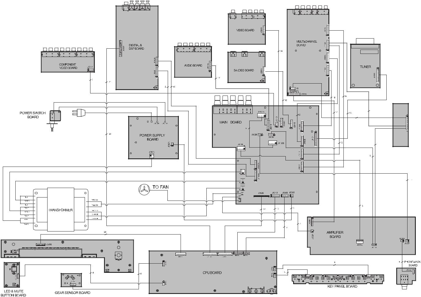
NOTE : MAIN ... etc. identifies each pcb module.
NOTE : MAIN ... etc. repères des platines constituant l'appareil.
HINWEIS : MAIN ... usw. Kennzeichnung der Platinen, aus denen das Gerät zusammengesetzt ist.
NOTA : MAIN ... ecc. sigla delle piastre dell' apparecchio.
NOTA : MAIN ... etc. marcas de las
placas que constituyen el aparato.
|
|
|
|
|
|
|
ENGLISH |
FRANÇAIS |
DEUTSCH |
ITALIANO |
ESPAÑOL |
|
|
|
|
|
|
|
|
|
|
|
|
1 |
|
|
|
|
|
|
AUDIO "R" |
AUDIO "D" |
AUDIO "R" |
AUDIO "D" |
AUDIO "D" |
|
|
|
|
|
|
||||||
2 |
|
|
|
|
|
|
AUDIO "R" |
AUDIO "D" |
AUDIO "R" |
AUDIO "D" |
AUDIO "D" |
|
|
|
|
|
|
||||||
3 |
|
|
|
|
|
|
AUDIO "L" |
AUDIO "G" |
AUDIO "L" |
AUDIO "S" |
AUDIO "I" |
|
|
|
|
|
|
||||||
4 |
|
|
|
|
|
|
AUDIO |
AUDIO |
AUDIO |
AUDIO |
AUDIO |
|
|
|
|
|
|
||||||
|
|
|
|
|
|
||||||
5 |
|
|
|
|
|
|
"BLUE" |
"BLEU" |
"BLAU" |
"BLU" |
"AZUL" |
|
|
|
|
|
|
||||||
|
|
|
|
|
|
||||||
6 |
|
|
|
|
|
|
AUDIO "L" MONO |
AUDIO "G" MONO |
AUDIO "L" MONO |
AUDIO "S" MONO |
AUDIO "I" MONO |
|
|
|
|
|
|
||||||
7 |
|
|
|
|
|
|
"BLUE" |
"BLEU" |
"BLAU" |
BLU |
AZUL |
|
|
|
|
|
|
||||||
8 |
|
|
|
|
|
|
SLOW SWITCH |
COMMUT. LENTE |
AV |
"COMMUTAZIONE |
"CONMUTACION |
|
|
|
|
|
|
UMSCHALTUNG |
LENTA" |
LENTA" |
|||
9 |
|
|
|
|
|
|
"GREEN" |
"VERT" |
"GRÜN" |
"VERDE" |
"VERDE" |
|
|
|
|
|
|
||||||
|
|
|
|
|
|
||||||
10 |
NC |
|
|
|
|
|
|||||
11 |
|
|
|
|
|
|
"GREEN" |
"VERT" |
"GRÜN" |
"VERDE" |
"VERDE" |
|
|
|
|
|
|
||||||
12 |
NC |
|
|
|
|
|
|||||
13 |
|
|
|
|
|
|
"RED" |
"ROUGE" |
"ROT" |
"ROSSO" |
"ROJA" |
|
|
|
|
|
|
||||||
|
|
|
|
|
|
||||||
14 |
NC |
|
|
|
|
|
|||||
15 |
|
|
|
|
|
|
"RED" |
"ROUGE" |
"ROT" |
"ROSSO" |
"ROJA" |
|
|
|
|
|
|
||||||
16 |
|
|
|
|
|
|
FAST SWITCH |
COMMUT. RAPIDE |
AUSTASTUNG |
"COMMUTAZIONE |
"CONMUTACION |
|
|
|
|
|
|
RAPIDA" |
RAPIDA" |
||||
|
|
|
|
|
|
|
|||||
17 |
|
|
|
|
|
|
VIDEO |
VIDEO |
VIDEO |
VIDEO |
VIDEO |
|
|
|
|
|
|
||||||
|
|
|
|
|
|
|
|
|
|
|
|
18 |
|
|
|
|
|
|
FAST SWITCH |
COMMUT. RAPIDE |
AUSTASTUNG |
"COMMUTAZIONE |
"CONMUTACION |
|
|
|
|
|
|
||||||
|
|
|
|
|
|
RAPIDA" |
RAPIDA" |
||||
|
|
|
|
|
|
|
|||||
19 |
|
|
|
|
|
|
VIDEO |
VIDEO |
VIDEO |
VIDEO |
VIDEO |
|
|
|
|
|
|
||||||
20 |
|
|
|
|
|
|
VIDEO OR "SYNC" |
VIDEO SYNCHRO |
VIDEO ODER |
VIDEO O SINCRO |
VIDEO O SINCRO |
|
|
|
|
|
|
SYNCHRO |
|||||
21 |
|
|
|
|
|
|
PLUG SCREEN |
BLINDAGE PRISE |
ABSCHIRMUNG |
INVOLUCRO METAL- |
BLINDAJE |
|
|
|
|
|
|
BOX |
DES STECKERS |
LICO DELLA PRESA |
DEL ENCHUFE |
||
: INPUT - ENTRÉE - EINGANG - ENTRATA - ENTRADA • |
|
: OUTPUT - SORTIE - AUSGANG - USCITA - SALIDA • |
|
|
: EARTH - MASSE - MASSE - MASSA - MASA |
|
|
|
|
|
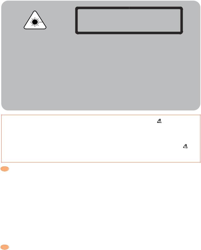
CLASS 1 LASER PRODUCT |
|
|
|
APPAREIL A LASER DE CLASSE 1 |
|
|
|
LASER KLASSE 1 |
|
|
|
APPARECCHIO CON LASER DI CLASSE 1 |
|
|
|
APARATO CON LASER DE CLASE 1 |
|
|
|
|
|
DANGER : |
Invisible laser radiation when open and interlock failed |
||
|
or defeated. Avoid direct exposure to beam. |
||
ATTENTION : |
Le rayon laser est invisible. Eviter l'exposition directe |
||
|
lors de la maintenance. |
||
VORSICHT BEI |
Bei geöffneter Schublade und Defekt der Sicherheits- |
||
REPARATUREN : |
vorrichtungen besteht die Gefahr unsichtbaren |
||
|
Laserlichts. Niemals direkt in den Laserstrahl sehen. |
||
ATTENZIONE : |
Il raggio laser è invisible. Evitare l'esposizione diretta |
||
|
durante la manutenzione. |
||
IMPORTANTE : |
El rayo laser es invisible. Evitar la exposición directa |
||
|
en el momento del mantenimiento. |
||
IMPORTANT SAFETY NOTICE
There are special components used in this equipment which are imporant for safety, these part are marked by  symbol on the schematic circuit diagrams and replacement part list. It is essential that these safety critical components are replaced with the manufacture’s specified parts to prevent electric shock, fire, or other hazards. do not attempt to modify the original design without permission of the manufacturer.
REMARQUES DE SECURITE IMPORTANTE
AVISO IMPORTANTE SOBRE SEGURIDAD
En este equipo se utilizan componentes especiales que son muy importantes para la seguridad, están marcados con el símbolo  en los esquemas eléctricos y en las listas de repuestos. Es fundamental que estos componentes críticos de seguridad, sean reemplazados por las piezas originales indicadas por el fabricante para evitar los peligros de electrocución, de fuego, etc. y no modificar el diseñ o original sin autorización del fabricante.
EN Prevention of electro static discharge (esd) to Electrostatically Sensitive Devices (ESD)
Some semiconductor devices can be damaged easily by static electricity (integrated circuits, some field-effect transistors and semiconductor chip components. The following techniques should be used to help reduce the incidence of component damage caused by static electricity.
1.Immediately before handling any semiconductor component or semiconductor-equipped assembly, drain off any electrostatic charge on your body by touching a known earth ground or wear a discharging wrist strap device, which should be removed for potential shock reasons prior to applying power to the unit under test.
2.After removing an electrical assembly equipped with ESD devices, place the assembly on a conductive surface such as aluminum foil.
3.Use only a grounded-tip soldering iron to solder or unsolder ESD devices.
4.Use only an anti-static solder removal devices.
5.Do not use freon-propelled chemicals.
6.Do not remove a replacement ESD device from its protective package until immediately before your are ready to install it.
7.Immediately before removing the protective materials from the leads of a replacement ESD device, touch the protective material to the chassis or circuit assembly into which the device will be installed.
CAUTION : Be sure no power is applied to the chassis or circuit, and observe all other safety precautions.
8.Minimize bodily motions when handling unpackaged replacement ESD devices
ES Prevención contra descargas electro-státicas (esd) para los DISPOSITIVOS SENSIBLES electrostáticamente (ESD)
Algunos dispositivos semiconductores, pueden ser dañados fácilmente por la electricidad estática (los circuitos integrados, alg unos transistores de Efecto de Campo y los semiconductores "chip"). Las siguientes técnicas pueden ser utilizadas para ayudar a reducir la destrucción de los componentes causada por la electricidad estática.
1.Inmediatamente antes de manejar cualquier componente semiconductor o conjunto equipado con semiconductores, elimine la carga electrostática de su cuerpo tocando alguna toma de tierra conocida o utilizar una correa conductora conectada a una toma de tierra que
se pone en la muñeca la cual debe ser quitada (por razones de seguridad) antes de conectar la alimentación al equipo bajo prue ba.
2.Después de quitar un conjunto equipado con componentes ESD, coloque el conjunto sobre una superficie conductora, como papel aluminio.
3.Utilizar únicamente soldadores con la punta conectada a la toma de tierra para soldar o desoldar componentes ESD.
4.Utilizar solamente soldadores antiestáticos para quitar componentes.
5.No utilizar productos químicos con gas freón como propelente.
6.No sacar de su embalaje protector el nuevo componente ESD hasta inmediatamente antes de estar todo preparado para montarlo.
7.Inmediatamente antes de quitar los materiales de protección de las patillas del componente, tocar el material protector al chasis del conjunto donde se vaya a montar el componente.
CUIDADO : Asegúrese de que la alimentación no esté aplicada al chasis o circuito, y cumpla todas las precauciones de seguridad.
8.Maneje sin movimientos bruscos el componente ESD una vez desempaquetado.
RTDVD1
First issue 02 / 02
WIRING DIAGRAM - SCHEMA D'INTERCONNEXIONS - VERDRAHTUNGSPLAN - DIAGRAMMA DELLE INTERCONNESSIONI - ESQUEMA DE INTERCONEXIONES
2 |
LIMITER |
5 |
|
|
1 |
XJ3


 XJ2
XJ2


 XJ1
XJ1


 XJ4
XJ4


 J605B
J605B

 J8103
J8103
PAV5010
First issue 06 / 03 |
3 |
4 |
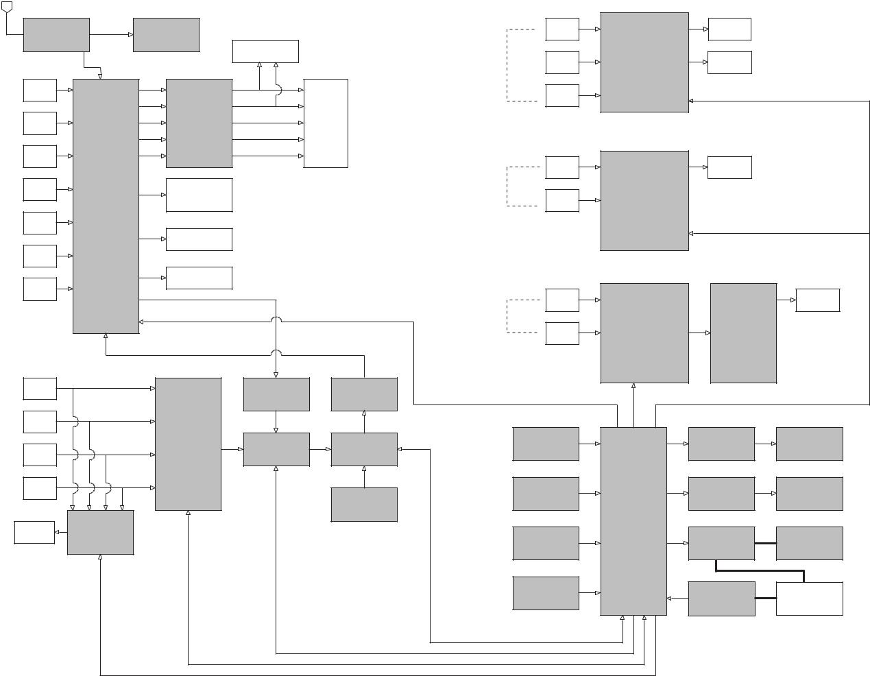
BLOCK DIAGRAM - SCHEMA SYNOPTIQUE - BLOCKSCHALTBILD - SCHEMA A BLOCCHI - ESQUEMA DE BLOQUES
FM ANT
LA 1837 |
|
LC 72131 PLL |
|
|
DVD |
|
VCR OUT |
|
|
AM/FM IF + MPX |
|
|
|
|
|
|
|||
|
|
|
|
|
|
|
|
||
|
|
|
|
HEADPHONE |
|
|
BA7625 |
|
|
|
|
|
|
|
COMPOSITE VIDEO |
VCR |
MON OUT |
|
|
|
|
|
|
|
VIDEO SELECTOR |
|
|||
CD |
|
FR |
|
FR |
|
SAT |
|
|
|
|
|
|
|
|
|
|
|
||
|
|
FL |
|
FL |
|
|
|
|
|
|
|
|
|
|
|
|
|
||
TV |
|
C |
POWER AMP |
C |
SPK OUT |
|
|
|
|
|
|
|
|
|
|
|
|||
|
|
SR |
|
SR |
|
|
|
|
|
SAT |
|
SL |
|
SL |
|
|
|
|
|
|
|
|
|
|
|
|
|
|
|
|
|
|
|
|
|
DVD |
|
MON OUT |
|
VCR |
M61516FP |
|
SUBWOOFER |
|
S-VIDEO |
|
BA7625 |
|
|
|
7.1 CH |
|
LINE OUT |
|
|
SAT |
|
|
|
|
ELECTRONIC |
|
|
|
VIDEO SELECTOR |
|
|
||
|
|
|
|
|
|
|
|
||
DVD |
VOLUME |
|
|
|
|
|
|
|
|
|
|
|
|
|
|
|
|
|
|
|
|
|
TAPE OUT |
|
|
|
|
|
|
TAPE |
|
|
|
|
|
|
|
|
|
5.1 CH |
|
|
VCR OUT |
|
|
|
|
|
|
|
|
|
|
|
|
|
|
|
|
EXT IN |
|
|
|
|
|
DVD |
|
|
MON OUT |
|
|
|
|
|
|
|
|
||
|
|
|
|
|
COMPONENT VIDEO |
|
|
BA7660FS |
|
|
|
|
|
|
|
|
74HC4052 |
|
|
|
|
|
|
|
|
SAT |
3-CH 75 OHM |
|
|
|
|
|
|
|
|
DUAL 4-CH MUX |
|
||
|
|
|
|
|
|
|
DRIVER |
|
|
|
|
|
|
|
|
|
|
|
|
OPT 1 |
|
|
|
CS5333 A/D |
CS4360 D/A |
|
|
|
|
|
|
|
|
|
|
|
|
||
OPT 2 |
|
|
|
|
|
|
|
|
|
|
|
|
CS8415 DIR |
74HC157 |
|
VOLUME |
|
LB1641 |
DOOR |
OPT 3 |
|
|
CS49326 DSP |
ENCODER |
|
MOTOR DRIVER |
|||
|
|
|
2CH SELECTOR |
|
|
||||
|
|
|
|
|
|
|
|
||
COAX |
|
|
|
|
|
REMOTE |
|
PT6305 |
VFD |
|
|
|
|
|
EEPROM |
SENSOR |
|
VFD DRIVER |
|
|
|
|
|
|
|
|
|||
|
|
|
|
|
W27C02 |
|
MCU M6759 |
|
|
|
|
|
|
|
|
|
|
|
|
OPT OUT |
74HC251 |
|
|
|
|
|
|
|
MAIN POWER |
|
|
|
|
|
|
KEY MATRIX |
|
RELAY |
|
|
|
|
|
|
|
|
SUPPLY |
||
|
|
|
|
|
|
|
|
|
|
|
|
|
|
|
|
EEPROM |
|
STANDBY |
|
|
|
|
|
|
|
AC24C16 |
|
AC INPUT |
|
|
|
|
|
|
|
|
POWER SUPPLY |
||
|
|
|
|
|
|
|
|
|
|
|
|
|
5 |
|
|
|
|
6 |
|
PAV5010
First issue 06 / 03
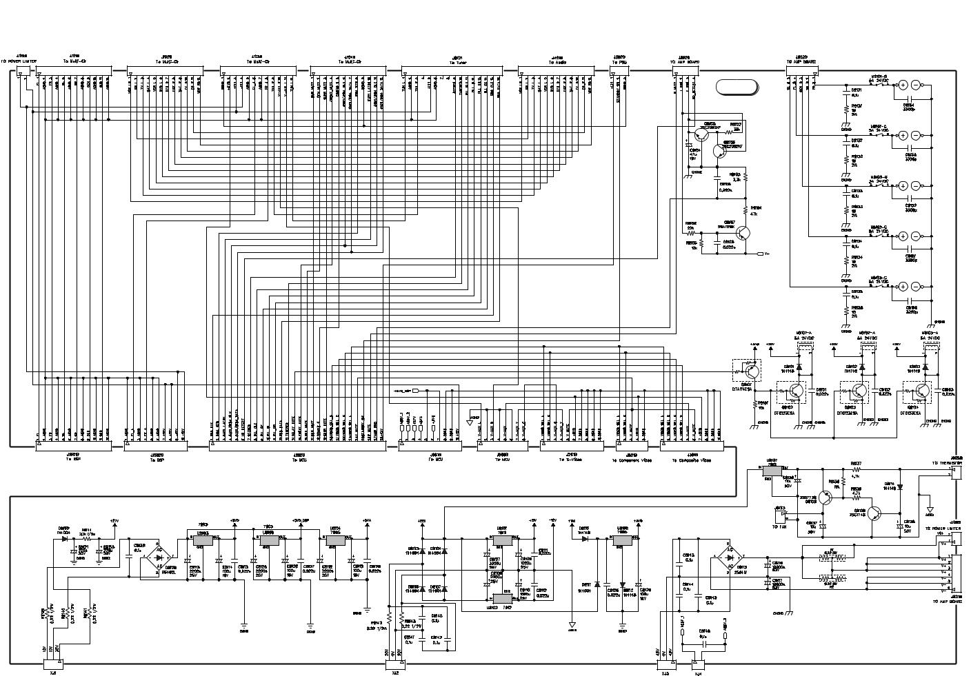
MAIN SCHEMATIC DIAGRAM - SCHEMA DE LA PLATINE PRINCIPALE - GRUNDPLATTE SCHALTBILD - SCHEMA DELLA PIASTRA PRINCIPALEESQUEMA DE LA PLATINA PRINCIPAL
MAIN
0.2
0.0 |
0.0 |
0.0 |
5.0 |
5.0 |
5.0 |
22.0 |
12.0 |
20.0
PAV5010
9 |
10 |
First issue 06 / 03 |
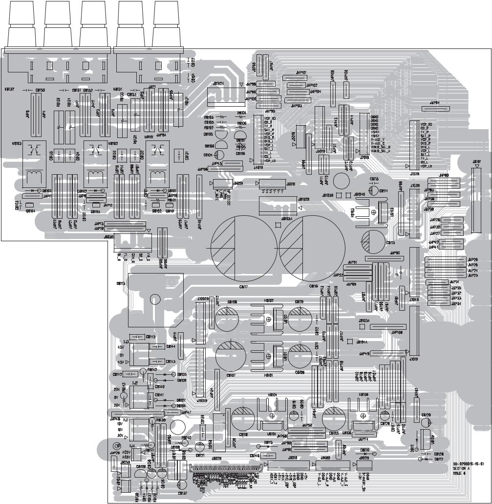
Main P.C.B.
Platine principale
Grundplatte
Piastra principale
Platina principal
E C B |
E C B |
E C B |
E C B |
C |
E |
B |
1 |
3 |
4 |
2 |
C |
|
B |
||
|
||
|
E |
|
|
C |
|
|
E |
|
|
B |
1 |
2 |
B |
E |
C |
3 |
4 |
B |
B |
E |
C |
B |
E |
C |
|
C |
E |
||||
|
|
|
B |
E |
C |
C |
E
B |
PAV5010
First issue 06 / 03 |
11 |
12 |
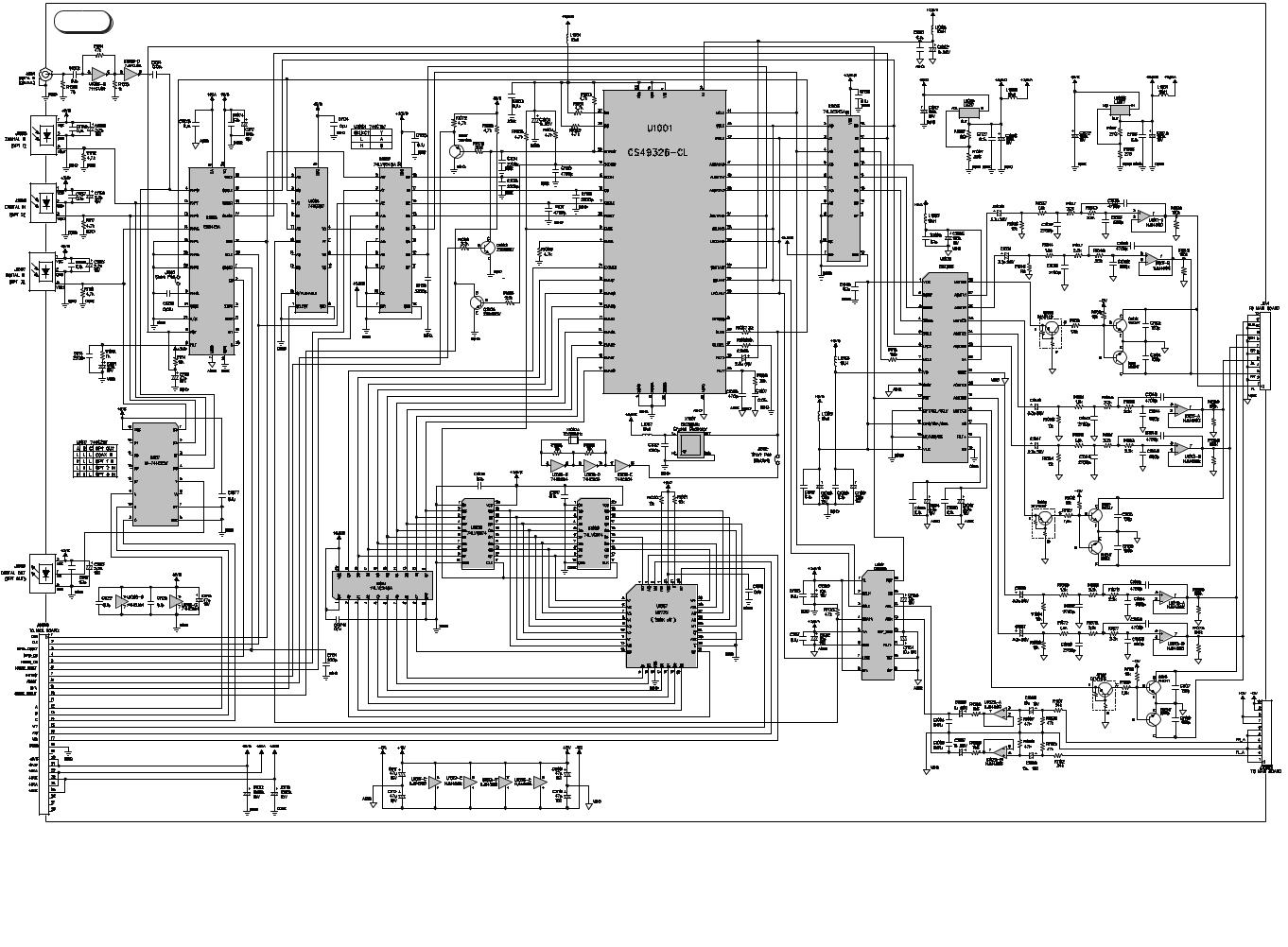
DIGITAL PROCESSING SCHEMATIC DIAGRAM - SCHEMA DU TRAITEMENT DIGITAL - SCHALTBILD DIGITALVERARBEITUNG - SCHEMA ELABORAZIONE DIGITALE - ESQUEMA DEL TRATAMIENTO DIGITAL
DSP
5.0 |
5.0 |
|
|
3.5 |
2.5 |
3.0 |
|
2.2 |
1.2 |
2.4 |
|
2.5
0.1 |
|
0.0 |
|
|
0.0 |
0.7 |
0.0 |
|
|
|
-12 |
|
0.0 |
|
0.0 |
0.0
PAV5010
13 |
14 |
First issue 06 / 03 |

Digital processing P.C.B.
Platine traitement digital
Ltpl. Digitalverarbeitung
Piastra elaborazione digitale
Platina tratamiento digital
ECB |
ECB |
ECB |
ECB |
ECB |
ECB |
ECB |
ECB |
ECB |
PAV5010
First issue 06 / 03
B |
C |
E |
B |
C |
E |
B |
C |
E |
15 |
Solder side |
Côté cuivre |
Lötseite |
Lato saldature |
Lado del cobre |
OUTADJ |
IN |
IN |
OUT |
ADJ |
OUTADJ |
IN |
IN |
OUT |
ADJ |
Component side
Côté composants
Bestückungsseite
Lato componenti
Lado componentes
16
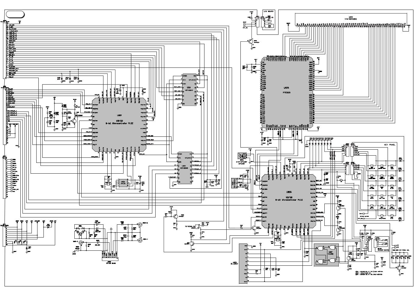
MICROCONTROLLER SCHEMATIC DIAGRAM - SCHEMA MICROCONTROLEUR - SCHALTBILD MICROCONTROLLERSTUFEN - SCHEMA MICROPROCESSORE - ESQUEMA MICROCONTROLADOR
MCU
PAV5010
17 |
18 |
First issue 06 / 03 |
 Loading...