


STRKS-600-PM
Table of contents
 Loading...
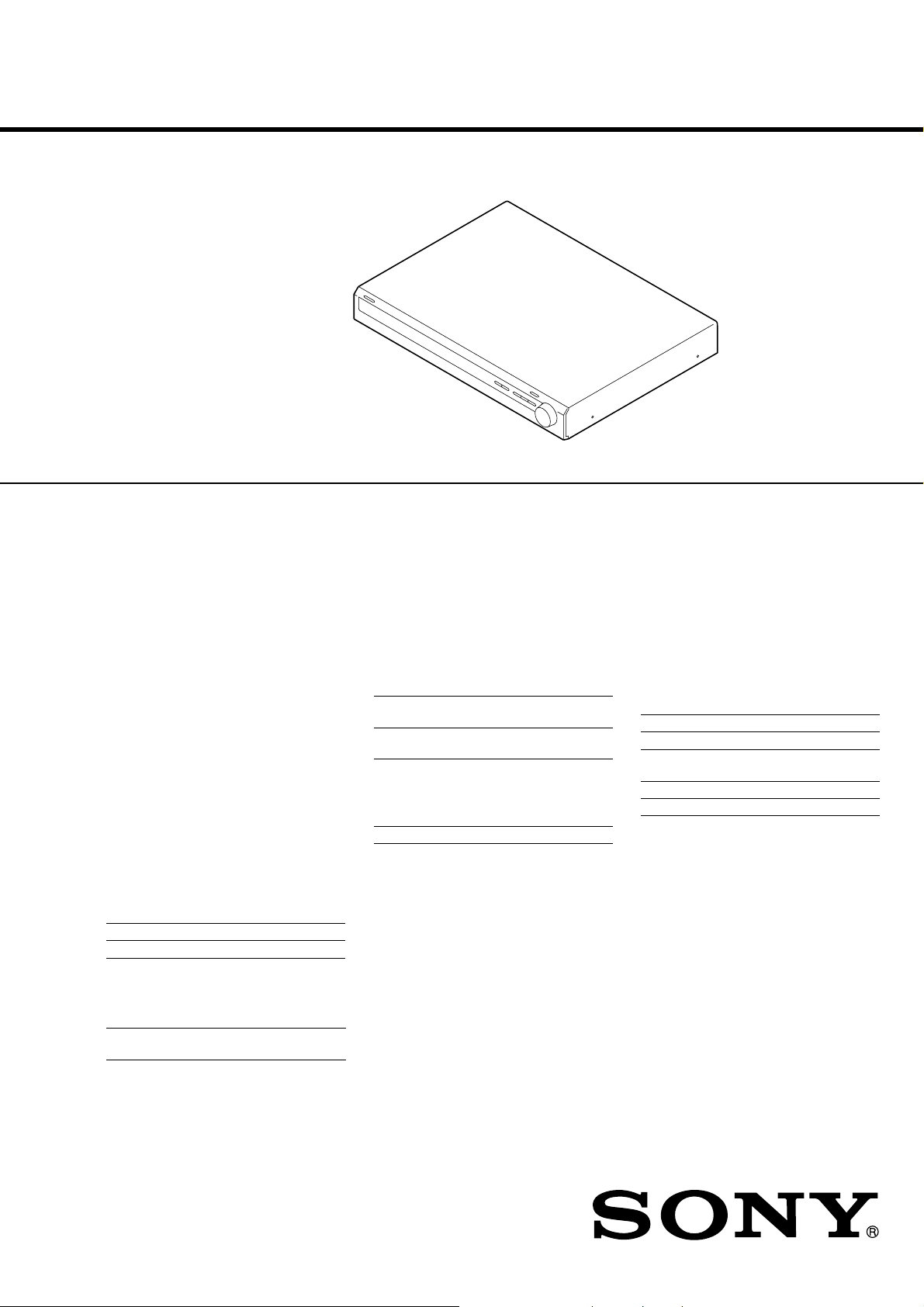
SERVICE MANUAL
Amplifier section
Power Output
1)
Models of area code CEL, CEK
(4 ohms 1 kHz, THD 0.7%)
FRONT
2)
: 70 W/ch
CENTER
2)
: 70 W
SURR
2)
: 70 W/ch
(4 ohms 100 Hz, THD 0.7%)
SUB WOOFER
2)
: 70 W
(4 ohms 1 kHz, THD 10%)
FRONT
2)
: 100 W/ch
CENTER
2)
: 100 W
SURR
2)
: 100 W/ch
(4 ohms 100 Hz, THD 10%)
SUB WOOFER
2)
: 100 W
1) Measured under the following conditions:
2) Depending on the sound field settings and the
source, there may be no sound output.
Inputs (Analog)
Inputs (Digital)
Reproduction frequency range:
28 – 20,000 Hz
Tone
FM tuner section
Tuning range 87.5 - 108.0 MHz
Antenna FM wire antenna
Antenna terminals 75 ohms, unbalanced
Intermediate Frequency 10.7 MHz
AM tuner section
Tuning range
Models of area code CEL, CEK
With 9-kHz tuning scale: 531 - 1,602 kHz
Antenna Loop antenna
Intermediate Frequency 450 kHz
General
Power req uirements
Power consumption
Power consumption (during standby mode)
0.3 W
Dimensions (w/h/d) (Approx.)
430 × 64 × 337 mm
including projecting parts
and controls
Mass (Approx.) 3.3 kg
Area code Power requirements
CEL, CEK 230 V AC, 50 Hz
SA-CD/CD, VIDEO 1, 2 Sensitivity: 1 V
Impedance: 50 kiloohms
DVD (Coaxial) Sensitivity: –
Impedance: 75 ohms
VIDEO 2, SA-CD/CD
(Optical)
Sensitivity: –
Impedance: –
Gain levels ±6 dB, 1 dB step
Area code Power requirements
CEL, CEK 230 V AC, 50/60 Hz
Area code Power consumption
CEL, CEK 110 W
Design and specifications are subject to change
without notice.
FM STEREO/FM-AM RECEIVER
AEP Model
STR-KS600PM/KS600PW
UK Model
STR-KS600PM
SPECIFICATIONS
STR-KS600PM/KS600PW
• STR-KS600PM is the receiver section in HT-SF800M.
• STR-KS600PW is the receiver section in HTP-32SS.
Ver. 1.1 2006.03
9-879-722-02
2006C05-1
© 2006.03
Sony Corporation
Home Audio Division
Published by Sony Techno Create Corporation
This receiver incorporates Dolby* Digital and Pro
Logic Surround and the DTS** Digital Surround
System.
* Manufactured under license from Dolby
Laboratories.
“Dolby”, “Pro Logic” and the double-D symbol are
trademarks of Dolby Laboratories.
**“DTS” and “DTS Digital Surround” are registered
trademarks of Digital Theater Systems, Inc.
– Continued on next page –

2
STR-KS600PM/KS600PW
TABLE OF CONTENTS
1. SERVICING NOTES ............................................... 3
2. GENERAL ................................................................... 4
3. DISASSEMBLY
3-1. Disassembly Flow ........................................................... 6
3-2. Case ................................................................................. 6
3-3. Front Panel Assy.............................................................. 7
3-4. SMPS Board .................................................................... 7
3-5. LINE FILTER Board ....................................................... 8
3-6. D-AMP Board ................................................................. 8
3-7. DIGITAL Board .............................................................. 9
4. TEST MODE.............................................................. 9
5. DIAGRAMS
5-1. Block Diagram – DSP Section – ..................................... 10
5-2. Block Diagram – AUDIO OUT Section –....................... 11
5-3. Block Diagram
– DISPLAY, POWER SUPPLY Section – ....................... 12
5-4. Printed Wiring Board
– DIGITAL Board (Component Side) – .......................... 14
5-5. Printed Wiring Board
– DIGITAL Board (Conductor Side) – ............................ 15
5-6. Schematic Diagram – DIGITAL Board (1/3) – ............... 16
5-7. Schematic Diagram – DIGITAL Board (2/3) – ............... 17
5-8. Schematic Diagram – DIGITAL Board (3/3) – ............... 18
5-9. Printed Wiring Board
– D-AMP Board (Component Side) – ............................. 20
5-10. Printed Wiring Board
– D-AMP Board (Conductor Side) –............................... 21
5-11. Schematic Diagram – D-AMP Board (1/2) – .................. 22
5-12. Schematic Diagram – D-AMP Board (2/2) – .................. 23
5-13. Printed Wiring Boards – DISPLAY Section –................. 24
5-14. Schematic Diagram – DISPLAY Section –..................... 25
5-15. Printed Wiring Board
– SPEAKER OUT, POWER SUPPLY Section (1/2) – ... 26
5-16. Printed Wiring Boards
– SPEAKER OUT, POWER SUPPLY Section (2/2) – ... 27
5-17. Schematic Diagram
– SPEAKER OUT, POWER SUPPLY Section – ............ 28
6. EXPLODED VIEWS
6-1. Cover Section .................................................................. 40
6-2. Chassis Block .................................................................. 41
7. ELECTRICAL PARTS LIST................................ 42
Notes on chip component replacement
• Never reuse a disconnected chip component.
• Notice that the minus side of a tantalum capacitor may be
damaged by heat.
SAFETY-RELATED COMPONENT WARNING!!
COMPONENTS IDENTIFIED BY MARK 0 OR DOTTED LINE
WITH MARK 0 ON THE SCHEMATIC DIAGRAMS AND IN
THE PARTS LIST ARE CRITICAL TO SAFE OPERATION.
REPLACE THESE COMPONENTS WITH SONY P ARTS WHOSE
PART NUMBERS APPEAR AS SHOWN IN THIS MANUAL OR
IN SUPPLEMENTS PUBLISHED BY SONY.
About area codes
The area code of the receiver you purchased is
shown on the lower portion of the rear panel ( see
the illustration below).
Any differences in operation, accordi ng t o the area
code, are clearly indicated in the text, for example,
“Models of area code AA only”.
FRONT R
– +
CENTER
– +
FRONT L
– +
SURR R
+ –
SUBWOOFER
+ –
SURR L
+ –
2-XXX-XXX-XX AA
Area code

3
STR-KS600PM/KS600PW
SECTION 1
SERVICING NOTES
NOTES ON REPLACEMENT OF THE DIGITAL BOARD
New part of EEPROM (IC1131) on the DIGITAL board cannot be
used. Therefore, if the mounted DIGITAL board (A-1097-941-A)
is replaced, exchange new microcomputer and new EEPR OM with
that used before the replacement.
UNLEADED SOLDER
Boards requiring use of unleaded solder are printed with the lead-
free mark (LF) indicating the solder contains no lead.
(Caution: Some printed circuit boards may not come printed with
the lead free mark due to their particular size)
: LEAD FREE MARK
Unleaded solder has the following characteristics.
• Unleaded solder melts at a temperature about 40 °C higher
than ordinary solder.
Ordinary soldering irons can be used but the iron tip has to be
applied to the solder joint for a slightly longer time.
Soldering irons using a temperature regulator should be set to
about 350 °C.
Caution: The printed pattern (copper foil) may peel away if
the heated tip is applied for too long, so be careful!
• Strong viscosity
Unleaded solder is more viscou-s (sticky, less prone to flow)
than ordinary solder so use caution not to let solder bridges
occur such as on IC pins, etc.
• Usable with ordinary solder
It is best to use only unleaded solder but unleaded solder may
also be added to ordinary solder.
4
STR-KS600PM/KS600PW
SECTION 2
GENERAL
This section is extracted from
instruction manual.
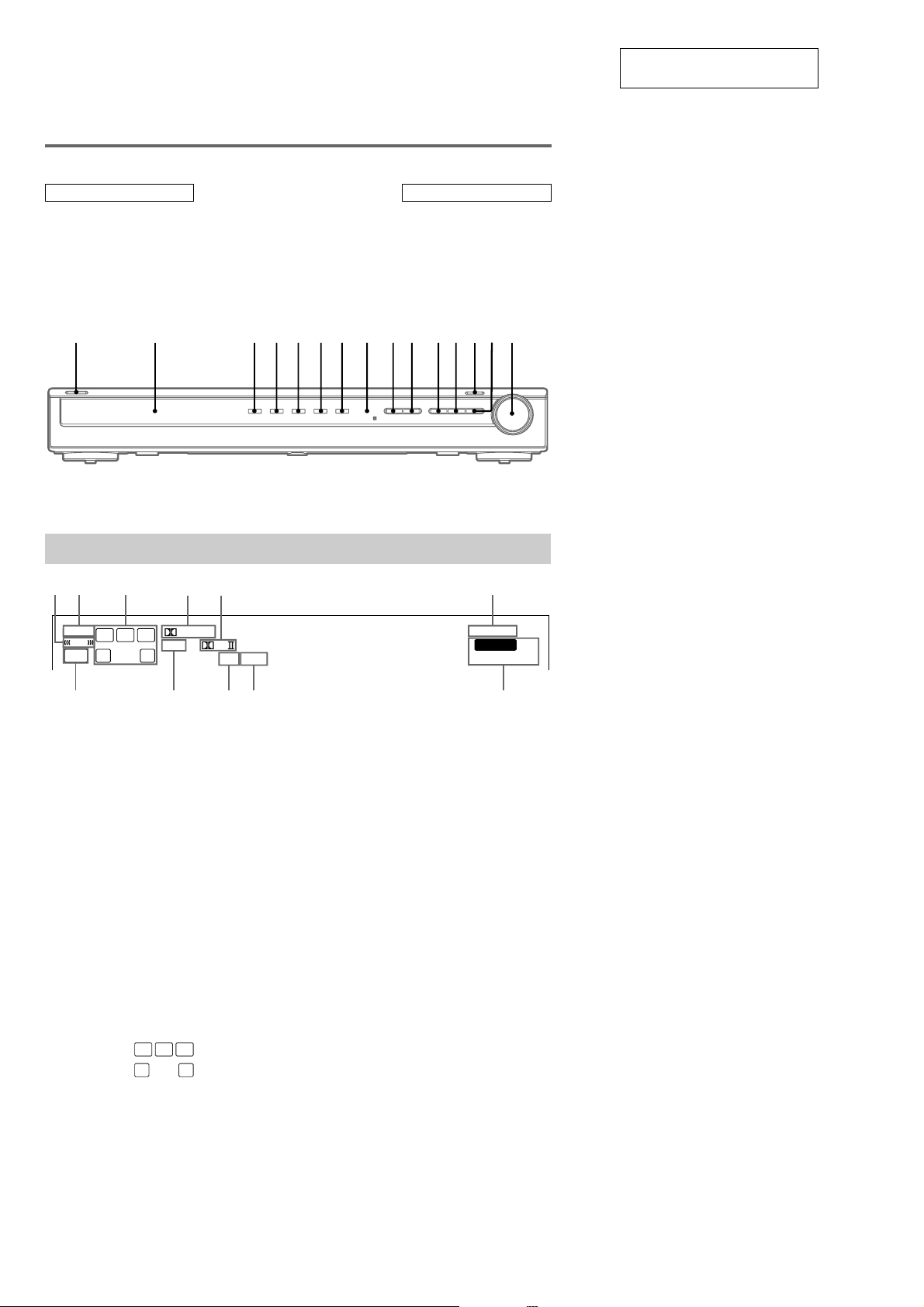
LOCATION OF CONTROLS
Main unit
Display 2
DVD (indicator) 5
INPUT SELECTOR
qd
IR (receptor) 8
MASTER VOLUME qg
MUTING qf
PRESET TUNING + q;
PRESET TUNING – 9
SA-CD/CD (indicator) 6
SOUND FIELD qs
TUNER (indicator) 7
VIDEO 1 (indicator) 3
VIDEO 2 (indicator) 4
?/1 (power) 1
; PLII qa
ALPHABETICAL ORDER
NUMBERS AND SYMBOLS
12 qd qgqs qfqaq;9876543
A LFE: Lights up whe n t he di sc be ing played
back contains the LF E (Low Frequency
Effect) channel and the LFE channel signal is
actually being reproduced.
B SLEEP: Lights up when sleep timer is
activated.
C Playback channel indicators: The letters
(L, C, R, etc.) indi cate the channels being
played back. The boxes around the letters vary
to show how the receiver downmixes the
source sound.
L (Front Left), R (Front Right), C (Center
(monaural)), SL (Surround Left), SR
(Surround Right), S (Surround (monaural or
the surround components obtaine d by Pro
Logic processing))
Example:
Recording format (Front /Surround): 3/2
Sound Field: A.F.D. AUTO
D ; DIGITAL: Lights up when the receiver is
decoding signals recorded in the Dolby Digital
format.
E ; PLII: “; PL” lights up when the receiver
applies Pro Logic processing to 2 channel
signals in order to output the center and
surround channel signals. “; PLII” lights up
when th e Pro Logic II Movie/Music decoder is
activated.
Note
Dolby Pro Logic and Dolby Pro Logic II
decoding do not function for DTS format signals.
F D.RANGE: Lights up when dynami c range
compression is activated.
G Tuner indicators: Lights up when using the
receiver to tune in radio stations, etc.
H COAX: Lights up when the source signal is a
digital signal being input through the COAX
terminal.
I OPT: Lights up when the source signal is a
digital signal being input through the OPT
terminal.
J DTS: Lights up when DTS signals are input.
K SW: Lights up when the audio signal is output
from the SUB WOOFER jack.
About the indications in the display
L
CR
SL S SR
SW
STEREO MONO
D. RANGE
MEMORY
DIGITAL
SLEEP
PL RDS
OPT COAX
LFE
DTS
78qa q; 9
213
4 5
6
L
CR
SL SR
5
STR-KS600PM/KS600PW
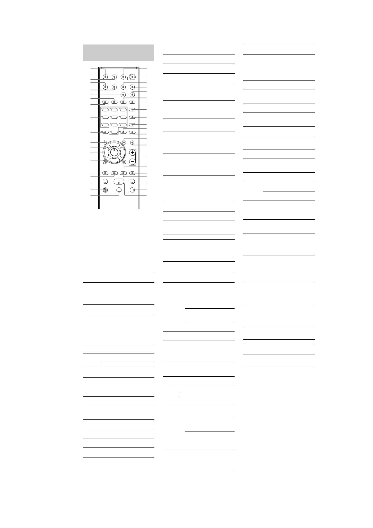
*TheMASTER VOL +, numeric button 5 and H
buttons have a ta c tile dot. Use the tactile dot as a
reference when operating the receiver and other
audio/video components.
Remote button
description
123
46
78
0/10
ENTER
9
SYSTEM STANDBY
TV/VIDEO
SLEEP
TEST
TONE
AV
?/1
VIDEO 1 VIDEO 2 DVD SA-CD/CD
2CH A.F.D.
RETURN/EXIT
TV CH –
PRESET –
TV CH +
PRESET +
TUNING –
TV
TUNING +
REPLAY ADVANCE
c STEP C
DISPLAY
MOVIE MUSIC
MEMORY SHIFT
D.SKIPCLEAR ANGLE
AV
MENU
TOP MENU/
GUIDE MUTING
TV VOL
MASTER VOL
FM MODE
MPX
AUDIO
D.TUNING
ANT
JUMP
SUBTITLE
DUAL MONO
TUNER
MAIN MENU
TV
?/1
?/1
>10
-
F
Gg
f
ENTER
.
HmM
Xx
<
<
>
5
1
3
2
4
ej
ek
el
eh
8
9
q;
qa
qs
qf
qd
qj
qh
qk
w;
wa*
ws
wd
wf
wh
wj
e;
wg
wk
wl
ea
*es
ef
eg
ql
qg*
5
6
7
ed
The tables below show the settings of each
button.
Remote
Button
Operations Function
A.F.D. ef Receiver Selects the decoding
mode for audio sound.
ANGLE
qs
DVD player Selects viewing angle or
changes the angles.
ANT 0 VCR/
Satellite tuner
Selects output signal
from the antenna
terminal: TV signal or
VCR program.
AUDIO
9
DVD player/
Satellite tuner
Changes the sound to
Multiplex or Bilingual
or Multi channel TV
sound.
AV
MENU qd
VCR/
DVD player/
Satellite tuner
Displays menu.
AV ?/1
1
VCR/
CD player/
DVD player/
Satellite tuner/
MD deck
Turns the audio and
video components on or
off.
CLEAR
ea
DVD player/
Satellite tuner
Clears a mistake when
you press the incorrect
numeric buttons or
returns to continuous
playback etc.
DISPLAY
qh
Receiver/
CD player/
VCR/
DVD player/
Satellite tuner/
MD deck
Selects information
displayed on the TV
screen.
D.SKIP
qa
CD player/
DVD player
Skips discs (multi-disc
changer only).
D.TUNING
0
Receiver Enters direct tuning
mode.
DUAL
MONO 8
Receiver Selects the language you
want during digital
broadcast.
DVD 3 Receiver To watch DVD.
ENTER
qa
TV/VCR/
Satellite tuner
After selecting a
channel, disc or track
using the numeric
buttons, press to enter
the value.
Remote
Button
Operations Function
ENTER wl Receiver/
VCR/
DVD player/
Satellite tuner/
CD player/
MD deck
Enters the selection.
FM MODE
9
Receiver Selects FM monaural
or stereo reception.
JUMP qs Satellite tuner Toggles between the
previous and the
current channels.
MAIN
MENU 5
Receiver Selects the menu of
the receiver.
MASTER
VOL +/–
qg
Receiver/TV Adjusts the master
volume of the
receiver.
MEMORY
qa
Receiver Stores the radio
stations.
MOVIE 6 Receiver Selects the pre-
programmed sound
fields for movie.
MPX 9 VCR Select main or sub
language.
MUSIC 7 Receiver Selects the pre-
programmed sound
fields for music.
MUTING qf Receiver Mutes the sound from
the receiver.
PRESET +/–
qjwh
Receiver Selects preset stations.
TV/VCR/
Satellite tuner
Select preset channel.
RETURN/
EXIT wj
DVD player Returns to the
previous menu or
exits the menu.
Satellite tuner Exits the menu.
SA-CD/CD
4
Receiver To listen to Super
Audio CD or compact
disc.
SHIFT qs Receiver Selects a memory
page for presetting
radio stations or
tuning to preset
stations.
Notes
•Some functions explained in this section may not
work depending on the model.
•The above explanation is intended to serve as an
example only. Therefore, depending on the
component the above operation may not be possible
or may operate differently than described.
•When you press input buttons (VIDEO 1, VIDEO 2
or DVD), the input mode of the TV might not switch
to the corresponding input mode that you want. In
this case, press TV/VIDEO button to switch the input
mode of the TV.
•To activate the buttons with orange print ing, press
TV and the button you want simultaneously.
.
Remote
Button
Operations Function
X ws VCR/
CD player/
DVD player/
MD deck/
Tape deck
Pauses playback or
recording. (Also starts
recording with
components in
recording standby.)
x w; VCR/
CD player/
DVD player/
MD deck/
Tape deck
Stops playback.
O wj DVD player Returns to the
previous menu or
exits the menu.
V/v wk Receiver Selects a menu item.
B/b wk Receiver Adjusts or changes
the setting.
V/v/B/b wk VCR/
Satellite tuner/
DVD player
Selects a menu item.
Remote
Button
Operations Function
SLEEP el Receiver Activates the sleep
function and the
duration which the
receiver turns off
automatically.
SUBTITLE
0
DVD player Changes the subtitles.
SYSTEM
STANDBY
(Press AV
?/1 1 and
?/1 2 at
the same
time)
Receiver/
TV/VCR/
CD player/
DVD player/
Satellite tuner/
MD deck
Turns off the receiver
and other Sony audio/
video components.
TEST
TONE ek
Receiver Outputs test tone.
TOP MENU/
GUIDE e;
DVD player Displays DVD title.
Satellite tuner Display guide menu.
TUNER eg Receiver To listen to radio
programs.
TUNING +/–
ql wf
Receiver Scans radio station.
TV wd TV To watch TV
programs.
TV CH +/–
qj wh
TV Selects preset TV
channels.
TV/VIDEO
el
TV Selects input signal:
TV input or video
input.
TV VOL
+/– qg
TV Adjusts the volume of
the TV.
TV ?/1 2 TV Turns the TV on or
off.
VIDEO 1
ej
Receiver To watch VCR.
(VTR mode 3)
VIDEO 2
eh
Receiver To watch VCR.
(VTR mode 1)
Remote
Button
Operations Function
1-9 and
0/10 es
Receiver Use with SHIFT to
preset radio station or
tuning to preset
stations and with
D.TUNING for
direct tuning.
CD player/
DVD player/
MD deck
Selects track
numbers.
0/10 selects track 10.
TV/VCR/
Satellite tuner
Selects channel
numbers.
2CH ed Receiver Selects 2CH
STEREO mode.
>10 ea VCR/
CD player/
DVD player/
Satellite tuner/
MD deck
Selects track
numbers over 10.
-/-- ea TV Selects the channel
entry mode, either
one or two digit.
?/1 2 Receiver Turns the receiver on
or off.
c
STEP
C
REPLAY /
ADVANCE
wg qk
VCR/
DVD player
Replay the previous
scene or fast forward
the current scene.
./>
wh qj
VCR/
CD player/
DVD player
Skips tracks.
m/M
wf ql
DVD player Searches tracks in the
forward or backward
direction.
VCR/
CD player/
MD deck/
Tape deck
Fastforwards or
rewinds.
H wa VCR/
CD player/
DVD player/
MD deck/
Tape deck
Starts playback.
<
<
STR-KS600PM/KS600PW
6
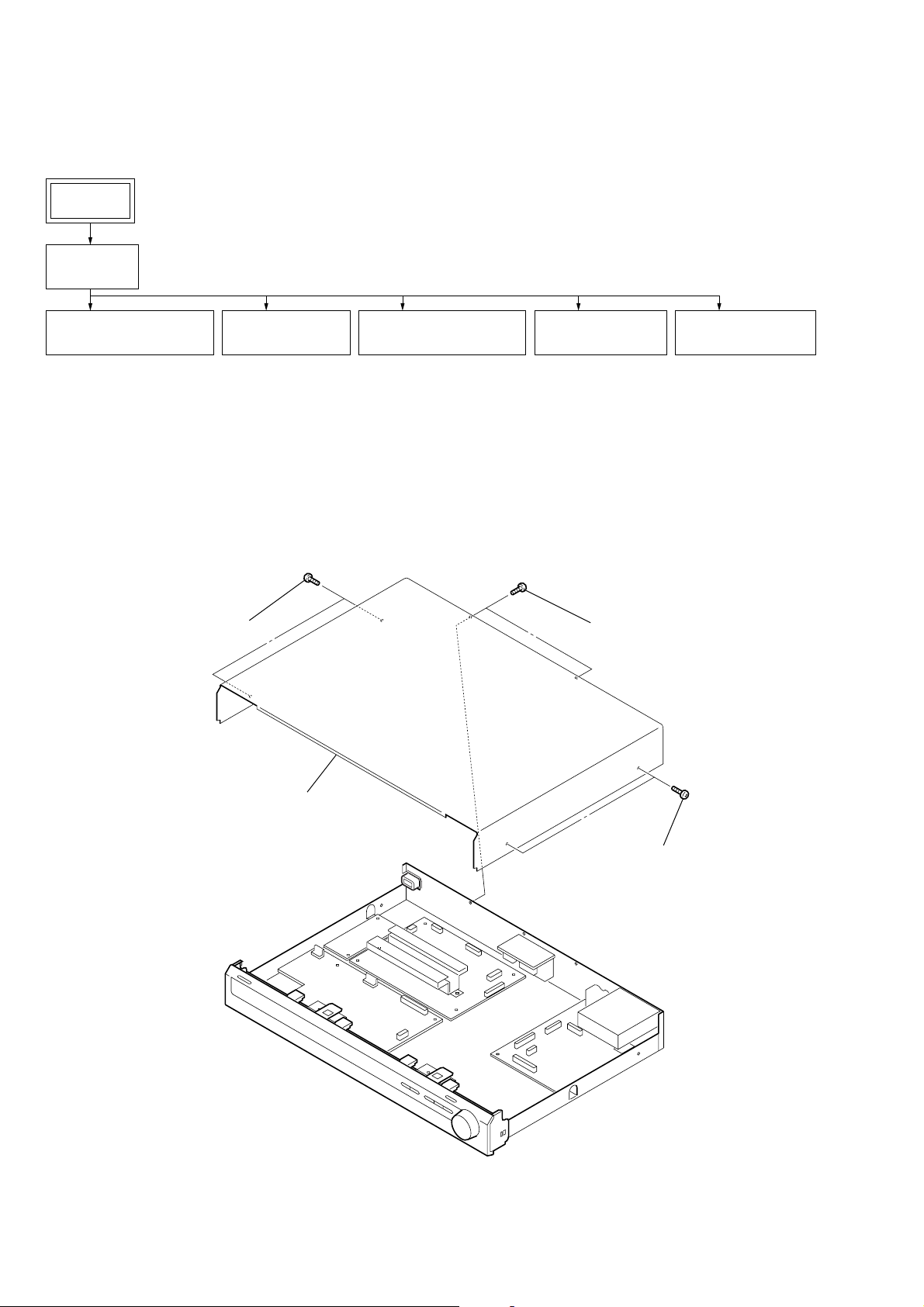
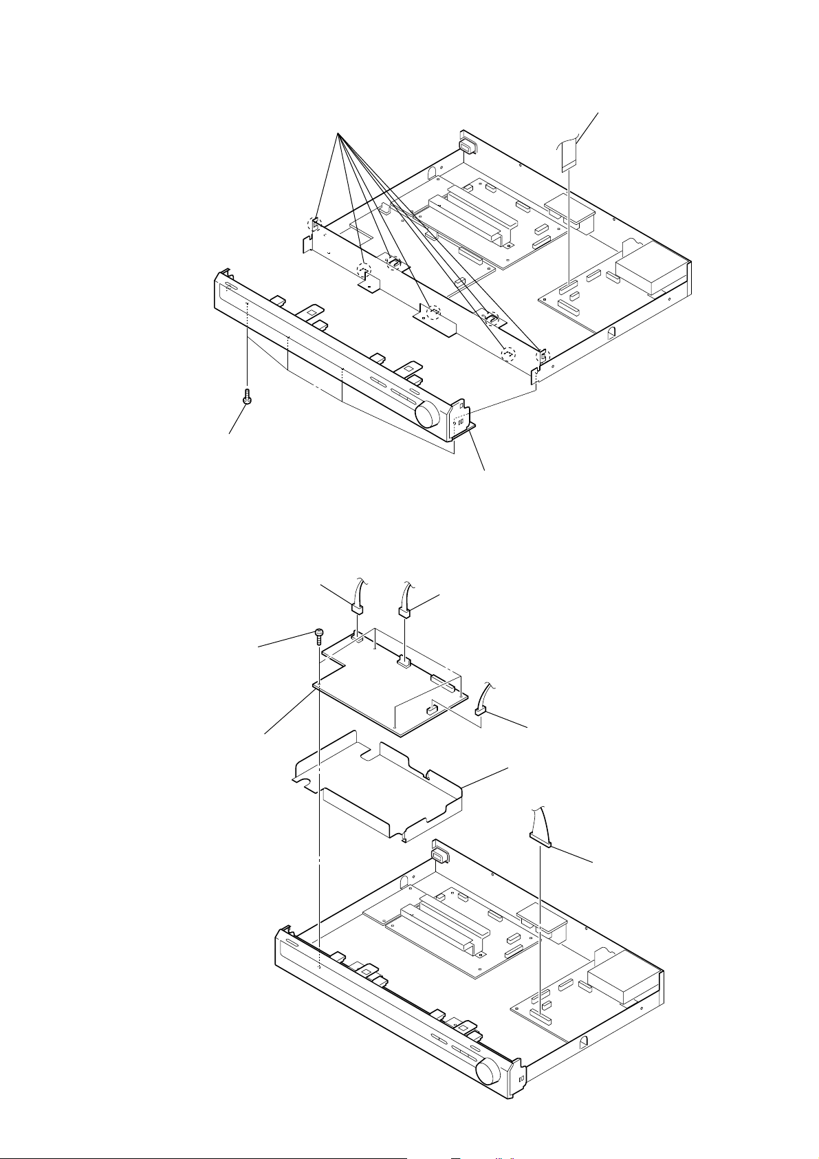
Note: Follow the disassembly procedure in the numerical order given.
3-2. CASE
• This set can be disassembled in the order shown below.
3-1. DISASSEMBLY FLOW
SECTION 3
DISASSEMBLY
3
two tapping screw
s
1
two screws
(BVTP3
×
8)
2
two tapping screws
4
case
3-2. CASE
(Page 6)
SET
3-3. FRONT PANEL ASSY
(Page 7)
3-4. SMPS BOARD
(Page 7)
3-5. LINE FILTER BOARD
(Page 8)
3-6. D-AMP BOARD
(Page 8)
3-7. DIGITAL BOARD
(Page 9)
STR-KS600PM/KS600PW
7
3-3. FRONT PANEL ASSY
3-4. SMPS BOARD
3
seven claws
1
wire (flat type) (17 core
)
(CNS193)
4
front panel assy
2
four screws
(BVTP3
×
8)
1
connector (CNP110)
7
sheet (SMPS)
2
connector (CNP811)
3
connector (CNP900)
4
connector (CNP901)
6
SMPS board
5
four screws
(BVTP3
×
6)
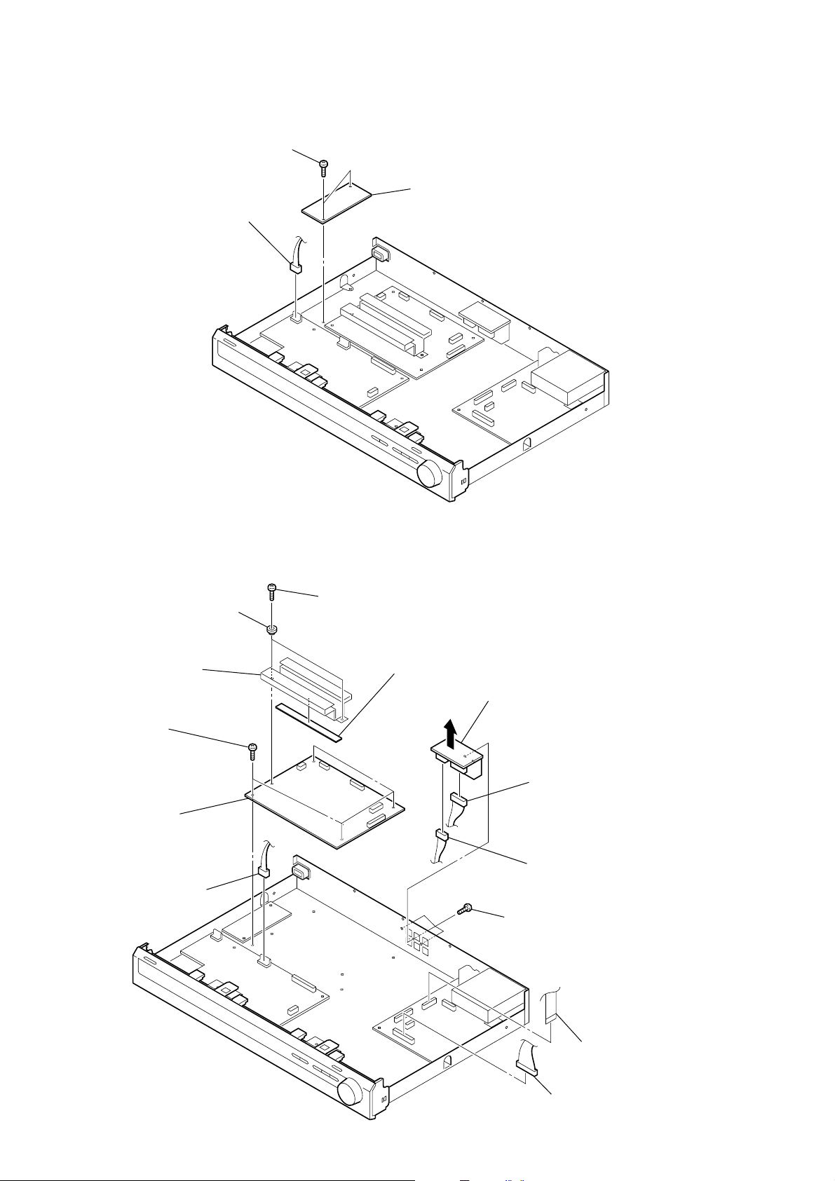
STR-KS600PM/KS600PW
8
3-5. LINE FILTER BOARD
3-6. D-AMP BOARD
0
two 03P insulating bushing
qa
heatsink assy
qs
radiation sheet
qd
four screws
(BVTP3
×
6)
qf
D-AMP board
5
SPK board
2
3
connector
(CNP500)
4
connector
(CNP510)
1
three screws
(BVTP3
×
8)
6
wire (flat type) (25 core)
(CNS1101)
7
connector
(CNP110)
9
two screws
(BVTP3
×
10)
8
connector (CNP900)
1
connector (CNP901)
3
LINE FILTER board
2
two screws
(BVTP3
×
6)
99
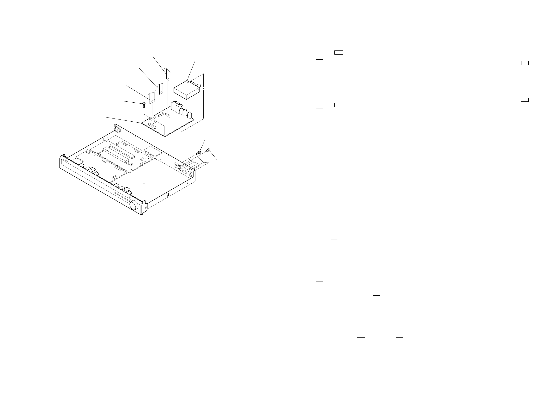
STR-KS600PM/KS600PW
STR-KS600PM/KS600PW
3-7. DIGITAL BOARD
2
three screw
s
(BVTP3
×
8)
6
five screws
(BVTP3
×
8)
8
DIGITAL board
7
two screws
(BVTP3
×
6)
5
wire (flat type) (17 core)
(CNS193)
4
wire (flat type) (25 core)
(CNS1101)
1
wire (flat type) (15 core)
(CNS195)
3
tuner
SECTION 4
TEST MODE
FACTORY PRESET MODE
All preset contents are reset to the default setting.
Procedure:
1. While pressing the PLII and [PRESET TUNING +] buttons,
press the I/1 button to turn on the main power.
2. The message “FACTORY” appears and the present contents
are reset to the default values.
ALL CLEAR MODE
All preset contents are cleared when this mode is activated. Use
this mode before returning the product to clients upon completion
of repair.
Procedure:
1. While pressing the PL II and [PRESET TUNING --] buttons,
press the I/1 button to turn on the main power.
2. The message “CLEARING !” appears and the memories are
reset to the default values.
3. When done, the message “CLEARED” appears.
FL CHECK MODE
All fluorescent segments are tested. When this test is activated, all
segments turn on at the same time, then each segment turns on one
after another.
Procedure:
1. While pressing the [MUTING] and [PRESET TUNING --] buttons,
press the I/1 button to turn on the main power.
2. All segments and all LEDs turn on.
3. Press the [INPUT SELECTOR] button.
4. Half of segments and [VIDEO 1], [SA-CD/CD] LEDs turn on.
5. Press the [INPUT SELECTOR] button once again.
6. Others half of segments and [VIDEO 2], [DVD] LEDs turn on.
7. Press the [INPUT SELECTOR] button once again.
8. All segments and all LEDs turn off.
VERSION MODE
When this mode is used, the model, the destination and the software
version number are displayed.
Procedure:
1. While pressing the [SOUND FIELD] and [PRESET TUNING --]
buttons, press the I/1 button to turn on the main power.
2. The model, the destination and the software version number
appear.
KEY CHECK MODE
This mode is used to check the key.
Procedure:
1. While pressing the [MUTING] and [INPUT SELECTOR] buttons,
press the I/1 button to turn on the main power.
2. The message “REST 06” appears.
3. Every pressing of any button other than the I/1 button counts
down the buttons. The b uttons which are already counted once
are not counted again.
4. When all buttons are pressed, the message “REST 00” appears.
PROTECTOR AUTO OFF MODE
When this mode is used, a protector on state is maintainable.
Procedure:
1. While pressing the [MUTING] and PLII buttons, press the I/1
button to turn on the main power.
2. The message “PROT EVER” appears.
SOUND FIELD CLEAR MODE
The preset sound field is cleared when this mode is activated. Use
this mode before returning the product to clients upon completion
of repair.
Procedure:
1. While pressing the [SOUND FIELD] button, press the I/1
button to turn on the main power.
2. The message “SF. CLR.” appears and initialization is
performed.
RDS AUTOBETICAL MODE
Procedure:
1. While pressing the [INPUT SELECTOR] button, press the I/1
button to turn on the main power.
2. The message “AUTO-BET” appears and scans and stores all
the FM and FM RDS stations in the broadcast area.
3. When done, the message “FINISH” appears.
1010
STR-KS600PM/KS600PW
STR-KS600PM/KS600PW
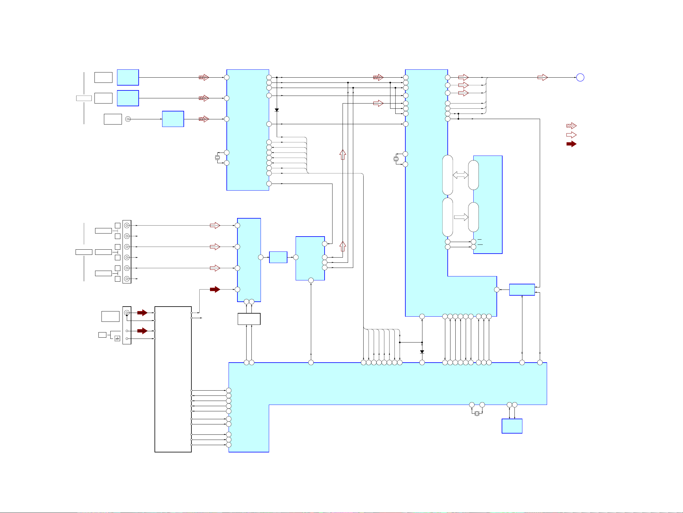
SECTION 5
DIAGRAMS
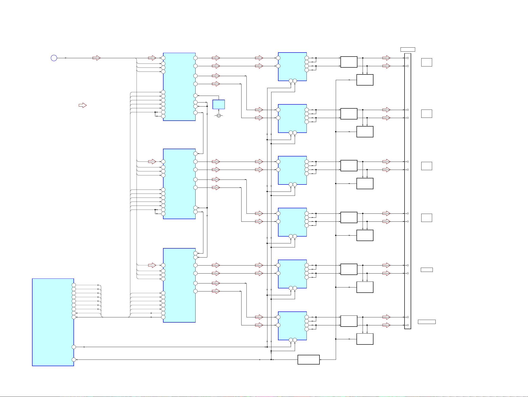
5-1. BLOCK DIAGRAM – DSP Section –
BOOT SELECT
IC1503
LEVEL SHIFT
Q1710, 1711
BUFFER
IC1600
EEPROM
IC1131
SYSTEM CONTROLLER
IC1601 (1/3)
OPTICAL
RECEIVER
IC1700
D1103
CS
6
10
A
9
B
X2
15
X0
12
X1
L CH
R CH
DO/ST
DI
14
X3
11
LIN
1
SDI2
30
BCKI2
29
LRCKI2
28
KFSIO
22
SDI1
18
BCKI1
17
AUDIO
69
LRCKI1
15
DIN0
3
D0
98
D1
97
CLK
95
CE
96
ERROR
99
ANA/DIG
24
18 19 20 4 5 2
7 6 9
XMODE
93
XSTATE
100
DATA0
1
AD_RST
10
SELECT_B
21
SELECT_A
22
88
EXLOCK
59
RSTB
6
CS0
44
SDO1
23
SDO2
24
SDO3
25
SCKOUT
14
BCKO
20
LRCKO
DATA1
DATA1 – DATA3,
SCK, BCK, LRCK
DATA2
DATA3
SCK
BCK
LRCK
19
GP10
67
DOUT
15
SYSCLK
16
BCK
14
LRCK
13
X
13
DO
35
DI
36
CLK
38
CKE
37
ERROR
34
XMODE
48
XSTATE
DIR DO
HDOUT
35
HDIN
33
HCLK
34
HCS
36
HACN
32
DECODE
68
PM
113
XRST
2
GP12
37
DIR DATA0
DIR DI
DIR CLK
DIR CE
DIR ERROR
DIR XMODE
DIR XSTATE
DIR DO
DIR DATA0
DIR DI
DIR CLK
DIR CE
DIR ERROR
DIR XMODE
DIR XSTATE
17
XMCLK
20
DATAO
16
BLK
14
LRCK
15
CKOUT
13
AUDIO
24
OPT IN
SA-CD/CD
OPTICAL
RECEIVER
IC1701
DIN1
4
OPT IN
VIDEO 2
SCHMITT
TRIGGER
IC1702
DIGITAL AUDIO
INTERFACE RECEIVER
IC1301
DIGITAL AUDIO
SIGNAL PROCESSOR
IC1501
DIN2
J1700
5
COAX IN
DVD
FM 75Ω
COAXIAL
86
85
87
89
53
52
43
66
65
WE
17
WE0
45
BST
56
DIGITAL
SA-CD/CD
VIDEO 2AUDIO IN
J1710
FM/AM TUNER PACK
TN1
VIDEO 1
AM
L
R
L
R
L
R
R-CH
R-CH
R-CH
ANALOG AUDIO
INPUT SELECT
IC1710
A/D CONVERTER
IC1602
S-RAM
IC1502
R-CH
21
22
X1301
12.288MHz
XOUT
XIN
9
12
X1502
13.9MHz
MCLK1
MCLK2
FM ANT
GND
AM ANT
GND
CLOCK
CE
MUTE
TUNED
STEREO
RDS DATA
RDS_CL
FM SIG OUT
T_DO
T. DATA
T. CLK
SLATCH
T_MUTE
TUNED
STEREO
RDS DATA
RDS CLK
RDS SIGNAL
108, 107, 105 – 102, 99,
98, 80 – 77, 75 – 72
7 – 10, 13 – 16,
29 – 32, 35 – 38
112, 110, 109, 97 – 92,
82 – 85, 66 – 64
D0 – D15A0 – A15
5 – 1, 44 – 42,
27 – 24, 21 – 18
D0 – D15
A0 – A15
D1301
HDOUT
HDIN
HCLK
HCS
HACN
GP9
PM
XRST
GP12
92
LRCK_SW
3
BST
82 83
X0
X1
34
SDA
33
SCL
X1101
24MHz
A
• SIGNAL PATH
: TUNER
: ANALOG INPUT
: DIGITAL INPUT
• R-ch is omitted due to same as L-ch.
(Page 11)
1111
STR-KS600PM/KS600PW
STR-KS600PM/KS600PW
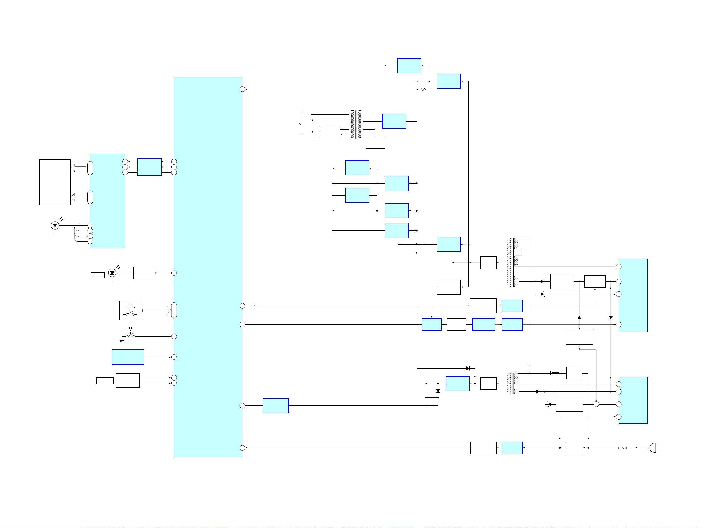
5-2. BLOCK DIAGRAM – AUDIO OUT Section –
• SIGNAL PATH
: AUDIO
/RST
/SD
4 13
DIGITAL POWER AMP
IC102
2
PWM_BP
TM500
(+)
(–)
29
OUT_B
25
OUT_A
30
OUT_B
26
OUT_A
STREAM PROCESSOR
IC108
31
DATA
36
XFSIIN
30
BCK
23
SCLATCH
27
INIT
19
SOFTMUTE
21
SCDT
29
LRCK
22
SCSHIFT
LATCH1
INIT
SOFTMUTE
SCDT
SHIFT
6
OUTR1
11
OUTL1
4
OUTR2
17
PWM_AP
9
OUTL2
38
FSOI
OVER LOAD
DETECT
Q103, 104
LOW-PASS
FILTER
FRONT
L
FRONT
R
SYSTEM CONTROLLER
IC1601 (2/3)
37
FSOCKO
48
XFSOIN
14
XFSOUT
SURR
L
SURR
R
CENTER
SPEAKERS
SUBWOOFER
DATA1
SCK
BCK
LRCK
INIT
LATCH1
LATCH2
LATCH3
SCDT
SHIFT
BUFFER
IC305
DATA1 – DATA3,
SCK, BCK, LRCKO
A
X450
49.152MHz
62
SCDT
61
SHIFT
60
LAT1
59
LAT2
58
LAT3
64
INT
SOFTMUTE
63
SOFT_MUTE
OVF
68
OVF
OVFW
78
OVFW
32
POWER_RST
26
POWER_SD
25
OVF FLAGL
OVF
24
OVF FLAGR
STREAM PROCESSOR
IC109
31
DATA
36
XFSIIN
30
BCK
23
SCLATCH
27
INIT
19
SOFTMUTE
21
SCDT
29
LRCK
22
SCSHIFT
LATCH1
INIT
SOFTMUTE
SCDT
SHIFT
6
OUTR1
11
OUTL1
4
OUTR2
9
OUTL2
38
FSOI
48
XFSOIN
14
XFSOUT
DATA2
SCK
BCK
LRCK
25
OVF FLAGL
OVF
24
OVF FLAGR
STREAM PROCESSOR
IC110
31
DATA
36
XFSIIN
30
BCK
23
SCLATCH
27
INIT
19
SOFTMUTE
21
SCDT
29
LRCK
22
SCSHIFT
LATCH1
INIT
SOFTMUTE
SCDT
SHIFT
6
OUTR1
11
OUTL1
4
OUTR2
9
OUTL2
38
FSOI
48
XFSOIN
DATA3
SCK
BCK
LRCK
25
OVF FLAGL
OVF
24
OVF FLAGR
OVFW
/RST
/SD
4 13
DIGITAL POWER AMP
IC101
2
PWM_BP
(+)
(–)
29
OUT_B
25
OUT_A
30
OUT_B
26
OUT_A
17
PWM_AP
OVER LOAD
DETECT
Q101, 102
LOW-PASS
FILTER
/RST
/SD
4 13
DIGITAL POWER AMP
IC104
2
PWM_BP
(+)
(–)
29
OUT_B
25
OUT_A
30
OUT_B
26
OUT_A
17
PWM_AP
OVER LOAD
DETECT
Q105, 106
LOW-PASS
FILTER
/RST
/SD
4 13
DIGITAL POWER AMP
IC103
2
PWM_BP
(+)
(–)
29
OUT_B
25
OUT_A
30
OUT_B
26
OUT_A
17
PWM_AP
OVER LOAD
DETECT
Q107, 108
LOW-PASS
FILTER
/RST
/SD
4 13
DIGITAL POWER AMP
IC105
2
PWM_BP
(+)
(–)
29
OUT_B
25
OUT_A
30
OUT_B
26
OUT_A
17
PWM_AP
OVER LOAD
DETECT
Q109, 110
LOW-PASS
FILTER
/RST
/SD
4 13
DIGITAL POWER AMP
IC106
2
PWM_BP
(+)
(–)
29
OUT_B
25
OUT_A
30
OUT_B
26
OUT_A
17
PWM_AP
OVER LOAD
DETECT
Q111, 112
LOW-PASS
FILTER
PROTECT DETCT
Q301
(Page 10)
1212
STR-KS600PM/KS600PW
STR-KS600PM/KS600PW
5-3. BLOCK DIAGRAM – DISPLAY, POWER SUPPLY Section –
3
SWITCHING REGULATOR
IC910
DRAIN
(AC IN)
MAIN POWER
TRANSFORMER
T910
SUB POWER
TRANSFORMER
T920
F901
VCC
D917
RECT
D902, 903
ISOLATOR
PC801
OSC
Q801, 802
B+ SWITCH
Q910
BUFFER
IC802
4
VCC
1
OCP
5
FB/OLP
8
SWITCHING REGULATOR
IC930
DRAIN
2
VCC
4
OCP/FB
5
START
RECT
D801
RECT
D830
ISOLATOR
PC803
ISOLATOR
PC802
SWITCHING
IC801
D932
D935
D831
D1006
STBY +4V
D930
+20V
REGULATOR
Q911
OVER CURRENT
DETECT
Q930
OVER CURRENT
DETECT
Q931
AC OFF DETECT
Q821, 822
POWER ON/OFF
CONTROL
Q820
+6V
REGULATOR
Q803
+31V
STBY +3.3V
+4V
REGULATOR
IC822
RESET SIGNAL
GENERATOR
IC1111
48STOP P. STOP
77RSTX
8PWM_DA
46P. CONT1
55FUSE DETECT
SYSTEM CONTROLLER
IC1601 (3/3)
RECT
D901
+
D934
D919, 920
TH901
+12V
+12V
REGULATOR
IC821
+7V
REGULATOR
IC1025
+3.3V
+3.3V
REGULATOR
IC820
ADC +5V
+5V
REGULATOR
IC1035
+2.6V
+2.6V
REGULATOR
IC1034
+5V
+5V
REGULATOR
IC1031
RDS +3.3V
+3.3V
REGULATOR
IC1711
+1.8V
+1.8V
REGULATOR
IC303
+9V
+9V
REGULATOR
IC1712
FL
FL
VEE
FOR FLUORESCENT
INDICATOR TUBE
DC/DC
CONVERTER
T700
RECT
D700 – 703
OSC
Q700, 701
72
FL_DATA
73
FL_CLK
74
FL_STB
FLUORESCENT
INDICATOR TUBE DRIVER,
LED DRIVER
IC700
7
DIN
8
CLK
9
STB
1
DVD LED
2
SA-CD/CD LED
3
VIDEO2 LED
4
VIDEO1 LED
D705 – 708
(PANEL INDICATOR)
FLUORESCENT
INDICATOR TUBE
FL700
SEG1 – SEG16
14 – 29
GRID1 – GRID12
42 – 31
54
SIRCS
ROTARY
ENCODER
RV700
LEVEL SHIFT
IC1651
REMOTE CONTROL
RECEIVER
IC701
VOLUME
38 – 40
A/D0 – A/D2
S701 – 705
56
POWER_KEY
70
VOLB
71
VOLA
67
TUNER_LED
D710
LED DRIVE
Q710
TUNER
S706
(POWER)
1313
STR-KS600PM/KS600PW
STR-KS600PM/KS600PW
• Note for Printed Wiring Boards and Schematic Diagrams
Note on Printed Wiring Board:
• X : parts extracted from the component side.
• Y : parts extracted from the conductor side.
• x : parts mounted on the conductor side.
•
f
: internal component.
• : Pattern from the side which enables seeing.
(The other layers' patterns are not indicated.)
• Indication of transistor
Caution:
Pattern face side: Parts on the pattern face side seen from
(Conductor Side) the pattern face are indicated.
Parts face side: Parts on the parts face side seen from
(Component Side) the parts face are indicated.
Note on Schematic Diagram:
• All capacitors are in µF unless otherwise noted. (p: pF)
50 WV or less are not indicated except for electrolytics
and tantalums.
• All resistors are in Ω and
1
/
4
W or less unless otherwise
specified.
• f : internal component.
• 2 : nonflammable resistor.
• 5 : fusible resistor.
• C : panel designation.
• A : B+ Line.
• B : B– Line.
• Voltages and waveforms are dc with respect to ground
under no-signal (detuned) conditions.
no mark : TUNER
• Voltages are tak en with a V OM (Input impedance 10 MΩ).
Voltage variations may be noted due to normal produc-
tion tolerances.
• Waveforms are taken with a oscilloscope.
Voltage variations may be noted due to normal produc-
tion tolerances.
• Circled numbers refer to waveforms.
• Signal path.
J : DIGITAL INPUT
F : ANALOG INPUT
f : TUNER
Note: The components identified by mark 0 or dotted line
with mark 0 are critical for safety.
Replace only with part number specified.
C
B
These are omitted.
E
Q
B
These are omitted.
CE
Q
• Circuit Boards Location
DIGITAL board
VOLUME board
DISPLAY board
SMPS board
LINE FILTER board
D-AMP board
SPK board
1414
STR-KS600PM/KS600PW
STR-KS600PM/KS600PW
R1120
X1101
R1166
IC1301
IC1502
IC1501
IC1601
R1089
IC1651
R1362
C1301
C1302
R1301
R1302
R1303
R1304
C1303
C1304
C1305
R1606
R1074
L1604
R1076
X1301
R1087
R1523
R1515
C1521
C1522
R1261
R1502
R1503
R1504
R1505
R1506
FB1503
R1073
R1151
R1305
R1311
R1360
R1306
R1307
R1178
R1170
R1171
R1172
R1173
R1174
R1190
R1183
R1159
R1124
R1129
R1105
R1186
R1122
R1123
R1119
R1126
R1125
R1180
R1053
R1056
R1529
R1308
R1309
D1301
R1312
R1313
R1315
R1316
R1136
R1137
R1134
R1135
R1041
R1140
R1142
R1143
R1144
IC1503
IC1034
R1160
R1161
R1162
R1121
R1150
R1501
R1149
IC1131
R1158
R1071
R1072
R1508
R1509
R1511
R1078
C1299
R1541
R1555
R1168
R1548
R1549
R1550
R1551
R1552
R1553
R1554
R1525
R1526
R1518
R1519
R1520
R1521
R1522
R1517
R1547
R1532
R1533
R1534
R1535
R1536
R1537
R1538
R1539
R1540
R1542
R1543
R1544
R1527
R1528
R1184
FB1305
IC1111
IC1602
R1127
R1189
C1107
C1137
R1128
R1604
R1260
FB1102
FB1302
FB1312
D1103
R1185
R1187
FB1502
R1188
R1167
FB1101
R1182
R1181
R1192
R1191
R1195
R1058
R1059
R1169
R1113
R1070
R1115
FB1501
C1033
IC1600
C1603
R1251
C1108
R1079
C1602
R1653
C1601
R1652
C1652
R1654
R1602
C1651
R1603
R1201
R1651
C1441
R1601
R1179
R1607
C1443
FB1511
R1044
C1483
FB1301
R1088
R1252
FB1308
R1175
R1608
X1502
IC1702
D1700
JR1101
JR1102
FB1700
FB1701
Q1710
Q1711
C1700
C1701
C1707
C1708
C1723
R1700
R1701
R1702
R1703
R1704
R1705
R1706
R1707
R1728
R1729
R1730
R1731
R1732
R1733
FB1702
FB1703
FB1704
FB1705
R1708
R1709
R1710
R1711
IC1710
D1001
L1600
C1705
31
30
1
30 1
112
36
37
48
24
13
25
61 90
91
120
60
31
51
80
50
10081
1-864-851-
11
(11)
DIGITAL BOARD
(COMPONENT SIDE)
E
E
1
3
5
4
13
2
A
B
C
D
E
F
G
1 2 3 4 5
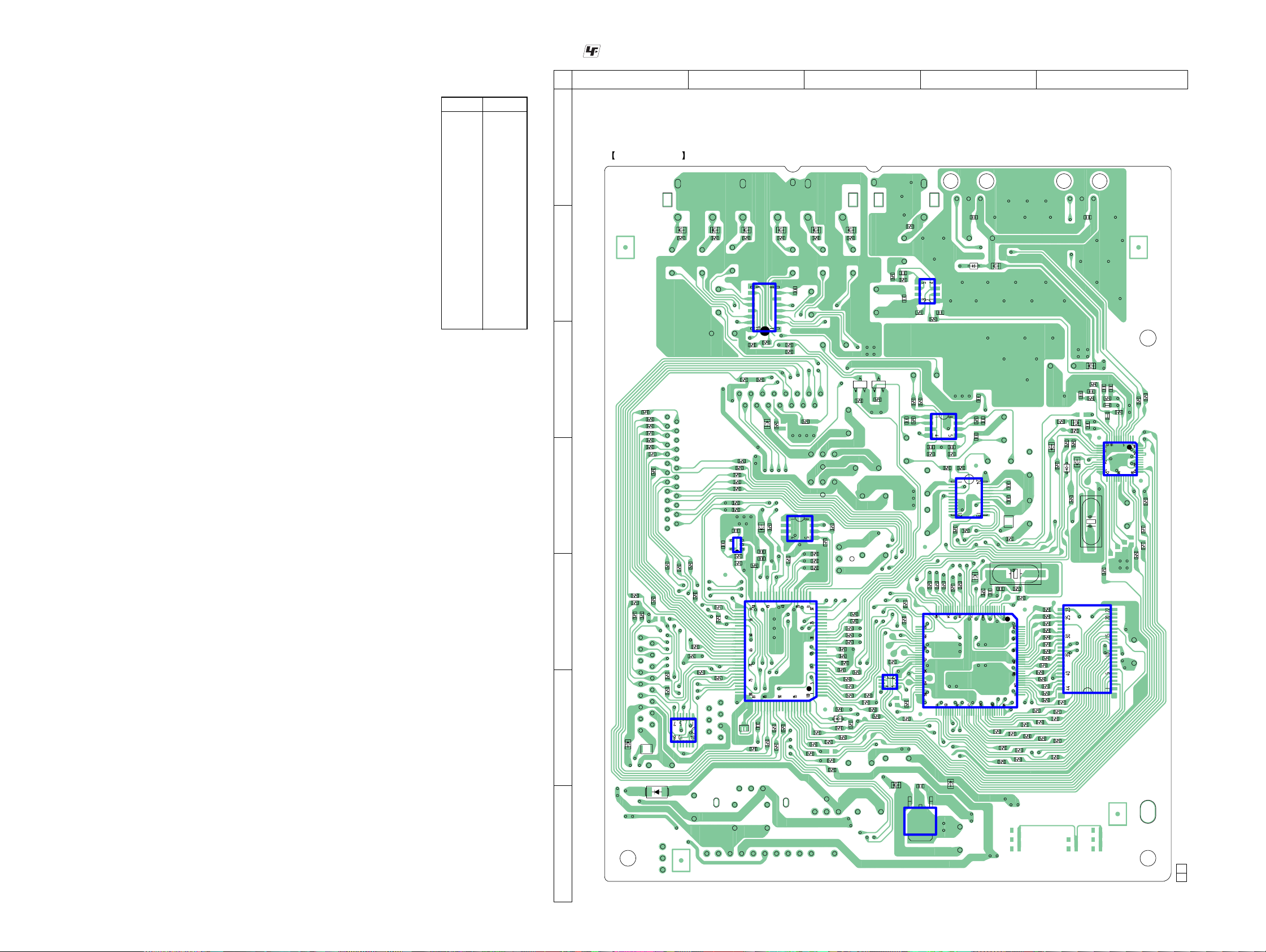
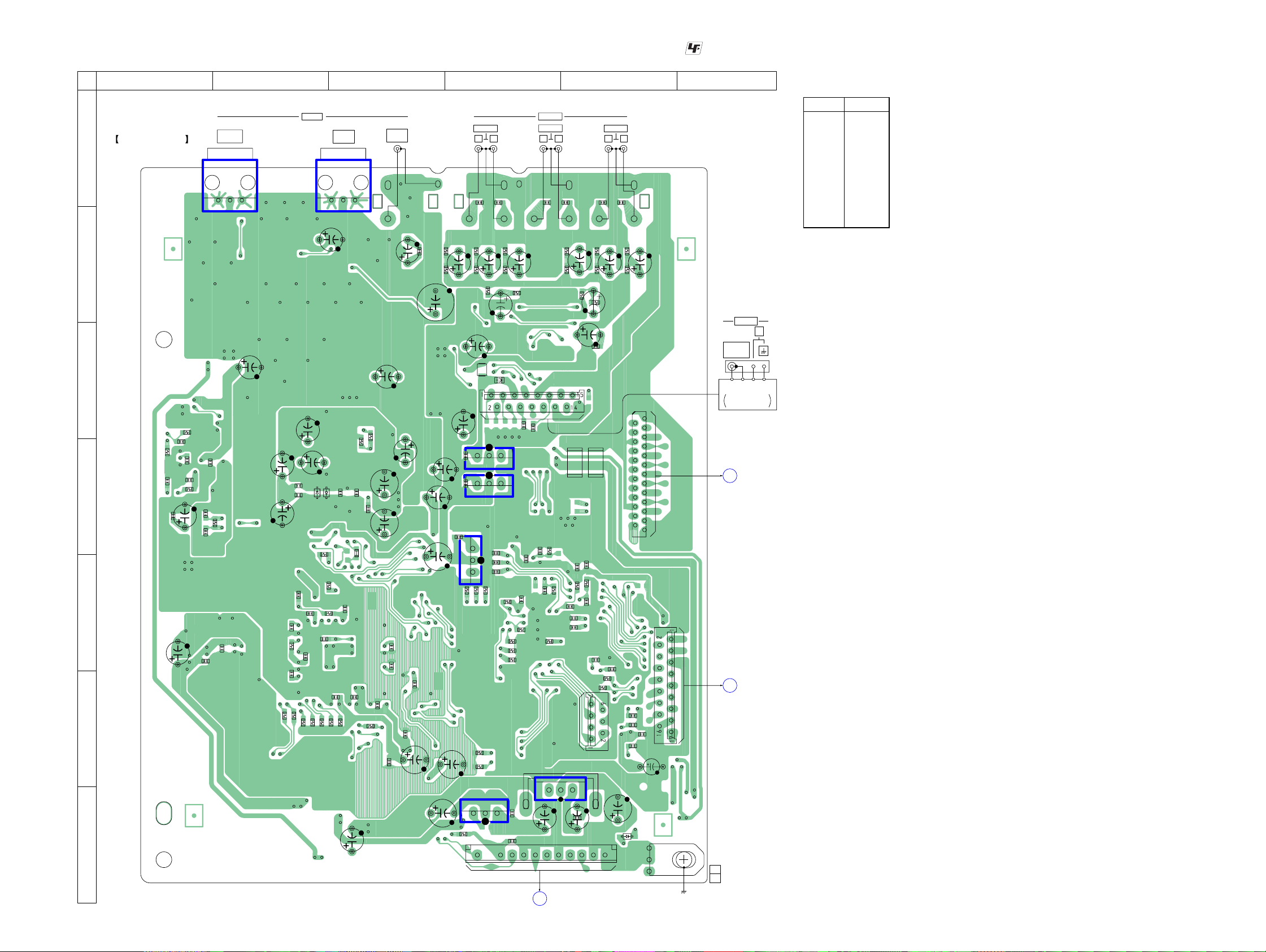
5-4. PRINTED WIRING BOARD – DIGITAL Board (Component Side) – • See page 13 for Circuit Boards Location.
: Uses unleaded solder.
D1001 G-1
D1103 F-3
D1301 D-5
D1700 B-4
IC1034 G-3
IC1111 D-2
IC1131 D-2
IC1301 D-5
IC1501 E-4
IC1502 E-5
IC1503 F-3
IC1600 C-4
IC1601 G-2
IC1602 D-4
IC1651 F-1
IC1702 B-4
IC1710 B-2
Q1710 C-3
Q1711 C-3
• Semiconductor
Location
Ref. No. Location
1515
STR-KS600PM/KS600PW
STR-KS600PM/KS600PW
5-5. PRINTED WIRING BOARD – DIGITAL Board (Conductor Side) –
• See page 13 for Circuit Boards Location. : Uses unleaded solder.
CNS195
CNS193
C1306
C1069
CNS192
C1525
C1515
C1032
C1656
IC1025
IC1035
C1036
C1024
C1026
C1035
C1936
C1605
C1655
C1610
C1653
C1604
C1654
CNP110
G1000
CNS1101
C1330
IC1031
IC1700
IC1701
IC1711
IC1712
J1700
J1710
C1702
C1703
C1706
C1716
C1721
C1724
C1725
C1726
C1727
C1728
C1730
C1732
C1717
C1718
C1715
C1720
C1719
C1517
C1504
R1091
R1092
C1607
C1138
C1502
R1049
C1505
R1096
R1097
R1086
R1082
R1085
R1083
R1570
R1081
C1142
C1121
C1122
R1193
C1123
C1124
C1125
C1105
R1636
C1104
R1546
R1545
R1556
C1620
R1635
C1657
R1314
C1310
C1309
C1308
C1312
C1313
C1314
C1315
R1317
R1318
C1609
C1067
C1031
R1513
R1571
R1572
R1573
R1574
C1508
C1507
C1506
C1503
C1501
C1509
C1510
R1514
C1511
R1512
C1513
C1514
C1519
C1520
C1516
C1518
C1066
C1100
C1068
C1025
C1034
R1163
C1163
C1252
C1102
C1129
C1130
R1054
R1055
C1065
C1251
R1610
C1659
C1404
R1043
R1605
D1003
FB1313
D1004
R1165
C1139
D1006
R1310
C1331
L1603
JR1010
JR1011
JR1104
C1704
C1709
C1710
C1722
C1729
C1731
R1715
R1716
R1721
R1722
R1724
R1725
R1726
R1727
C1711
C1712
C1713
C1714
R1717
R1723
R1713
R1720
R1719
R1714
R1712
R1718
JR1106
1
3
DIGITAL BOARD
(CONDUCTOR SIDE)
2
1
24
25
1-864-851-
11
(11)
(CHASSIS)
TN1
FM/AM TUNER PACK
SUPPLIED WITH THE
ASSEMBLED BLOCK
FM 75Ω
COAXIAL
ANTENNA
AM
DISPLAY BOARD
CNS703
C
SMPS BOARD
CN820
B
D-AMP BOARD
CNS301
A
NC
13
1
111
3
VIDEO 1
AUDIO IN
LR
VIDEO 2
LR
SA-CD/CD
COAX IN
DVD
OPT IN
VIDEO 2
OPT IN
SA-CD/CD
LR
DIGITAL
1313
13
13
A
B
C
D
E
F
G
1 2 3 4 5 6
D1003 D-2
D1004 D-2
D1006 G-5
IC1025 G-4
IC1031 G-4
IC1035 E-4
IC1700 A-2
IC1701 A-3
IC1711 D-4
IC1712 D-4
• Semiconductor
Location
Ref. No. Location
(Page 21)
(Page 24)
(Page 27)
1616
STR-KS600PM/KS600PW
STR-KS600PM/KS600PW
R
1
3
0
7
R
1
3
0
9
R1312
R1313
R1315
R
1
3
0
6
R1606
R1607
R1651
C1601
R1705
R
1
7
1
2
R
1
7
1
3
R
1
7
1
4
R
1
7
1
5
R
1
7
1
6
R
1
7
1
7
R
1
7
1
8
R
1
7
1
9
R
1
7
2
0
R
1
7
2
1
R
1
7
2
2
R
1
7
2
3
C1725
R1729
F
B
1
5
1
1
FB1313
F
B
1
3
0
5
C1700
C1701
C1703
R1702
R1703
C1705
IC1702
C1708
R1704
C1707
C1706
C1702
D1700
FB1308
R1362
R1700
C1301
C1305
C1306
R1301
R1302
R1304
C1304
C1303
R1303
C1302
R1314
C1331
C1330
C1308
R
1
3
6
0
C
1
3
0
9
C
1
3
1
0
F
B
1
3
0
1
R
1
3
0
8
D
1
3
0
1
R1305
C1603
C1609
R1605
C1604
C1653
C1659
R1603
C1656
C1654
R1653
IC1602
C1655
C1607
C1657
C1651
R1602
R1604
R1601
C1035
R1610
C1034
IC1600
R1311
FB1302
C1704
R1706
R1707
R1708
R1709
R1710
R1711
FB1705
FB1704
FB1703
FB1702
FB1701
FB1700
C1715
C1720
C1719
C1718
C1717
C1716
Q1711
C1252
R1261
R1260
C1732
C1731
IC1711
C1728 C1729
FB1312
C1251
C1441
R1727
D1003
D1004
CNS195
R1251
R1252
C1730
IC1301
R1701
R1652 R1654C1652
C1605
C1602
C1724
R1310
X
1
3
0
1
C
1
3
1
5
R
1
3
1
8
R1317
R1316
C1313
C1312
C1314
C1404
C1610
R1608
C1443
C1483
R1151
R1731
R1733
C1727
Q1710
R1728
R1732R1730
R1726
C1726
C1723
R1725C1721
R1724
C1722
C1709
C1710
C1711
C1712
C1713
C1714
IC1712
JR1101
JR1102
IC1035
IC1710
J1710
IC1700
IC1701
J1700
1
0
0
1
0
0
100
100
100
2
2
100
1k
10k
220p
100
1
0
k
1
0
k
1
0
k
1
0
k
1
0
k
1
0
k
1
0
k
1
0
k
1
0
k
1
0
k
1
0
k
1
0
k
10 50V
100
0.1
0.1
22
50V
1k
22k
1p
TC7WU04F
47p
560k
0.1
1000
6.3V
10
50V
1SS355TE-17
100
100
0.1
0.1
47 16V
5.6k
4.7k
100
0.01
0.1
33k
0.01
10k
0.1
10
50V
0.1
1
0
0
1
8
p
1
8
p
1
0
0
1
S
S
3
5
5
T
E
-1
7
470
0.1
0.1
4.7k
L1603
10µH
100
16V
10
50V0.1
3.3k
47 50V
47 50V
3.3k
PCM1800
10
50V
0.1
0.1
220p
470
1k
10k
470
10V
4.7k
0.1
NJM4565M(TE2)
100
0.1
1k
1k
1k
1k
1k
1k
10 50V
10 50V
10 50V
10 50V
10 50V
10 50V
DTC124EKA-T146
0.1
0
0
47
16V
0.1
TA78033LS
47
16V
0.1
0.1
0.0033
10k
ISS367-T3
ISS367-T3
15P
39k
39k
10
50V
LC89056W
75
10k 10k220p
10
50V
220p
100
16V
1M
1
2
.2
8
8
M
H
z
0
.1
1
0
k
10k
100
100p
0.1
0.1
0.1
L1604
10µH
47
16V
2.2k
470p
470p
100
10k
10k
10
50V
DTC124EKA-
T146
100
10k10k
10k
100
16V
0.1
10k100
16V
10k
0.1
100p
100p
100p
100p
100p
100p
TA7809
0
0
TA7805LS
MC14052 BDR2
TORX141
TORX141
A
1
A
2
A
3
A
4
A
5
A
6
A
8
A
9
A
1
0
A
1
2
B1
B2
B8
B3
B4
B5
B6
B7
A
1
3
A
1
1
D
A
T
A
O
X
S
T
A
T
E
CE
DI
DO
CLK
XMODE
T
_
M
U
T
E
L
A
T
T
D
A
T
D
O
T
C
L
K
RDS DATA
RDS_CL
FM SIG OUT
RDS(3.3V)
MUTE
R CH
GND
L CH
TUNED
VDD 10V
CE
DI
DO/ST
CLOCK
STEREO
+3.3V REGULATOR
+9V REGULATOR
OI
G
OI
G
A/D CONVERTER
DIGITAL AUDIO
INTERFACE RECEIVER
BUFFER
G
V
OI
G
+5V REGULATOR
V
G
SCHMITT TRIGGER
ANALOG AUDIO
INPUT SELECT
LEVEL SHIFT
LEVEL SHIFT
(CHASSIS)
L
R
L
R
L
R
SA-CD/CD
VIDEO 2
VIDEO 1
AUDIO IN
(CHASSIS)
COAX IN
DVD
(1/3)
OPTICAL RECEIVER
OPTICAL RECEIVER
OPT IN
SA-CD/CD
OPT IN
VIDEO 2
DIGITAL
AM
COAXIAL
FM 75Ω
THE ASSEMBLED
BLOCK
SUPPLIED WITH
FM/AM
TUNER PACK
TN1
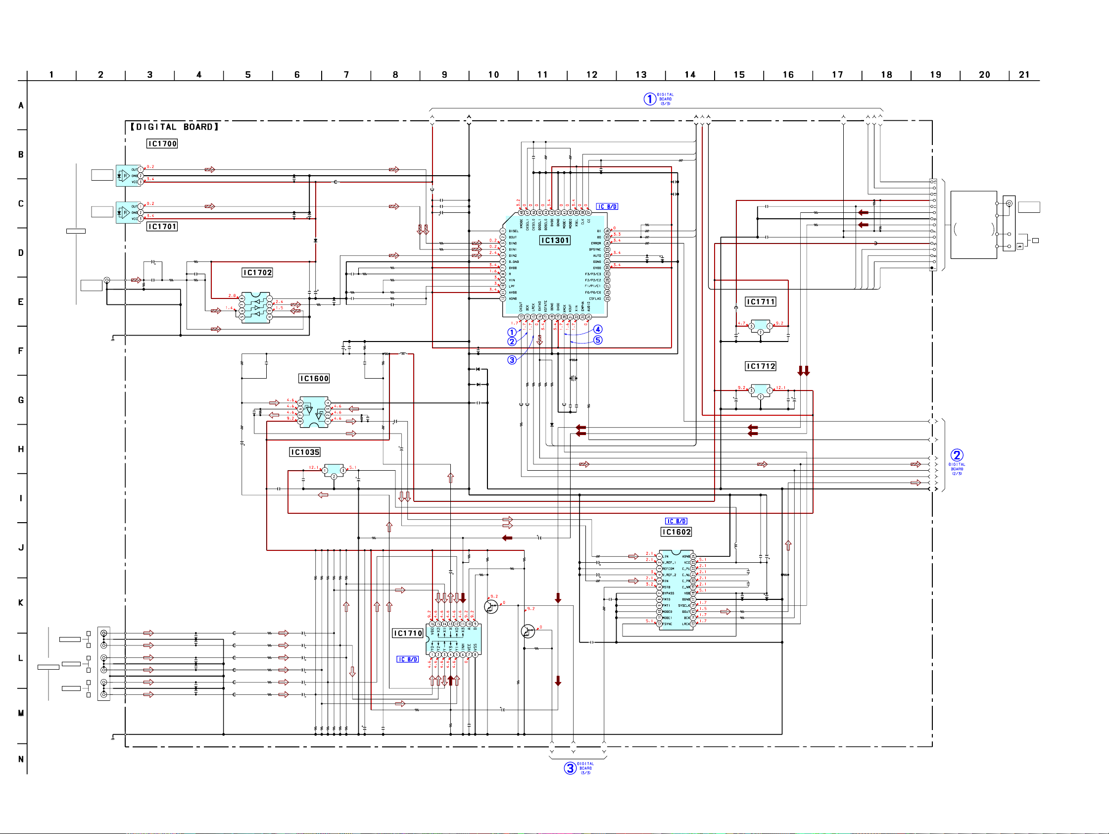
• See page 19 for Waveforms. • See page 29 for IC Block Diagrams. • See page 34 for IC Pin Function Description.
5-6. SCHEMATIC DIAGRAM – DIGITAL Board (1/3) –
(Page 18)
(Page 17)
(Page 18)
1717
STR-KS600PM/KS600PW
STR-KS600PM/KS600PW
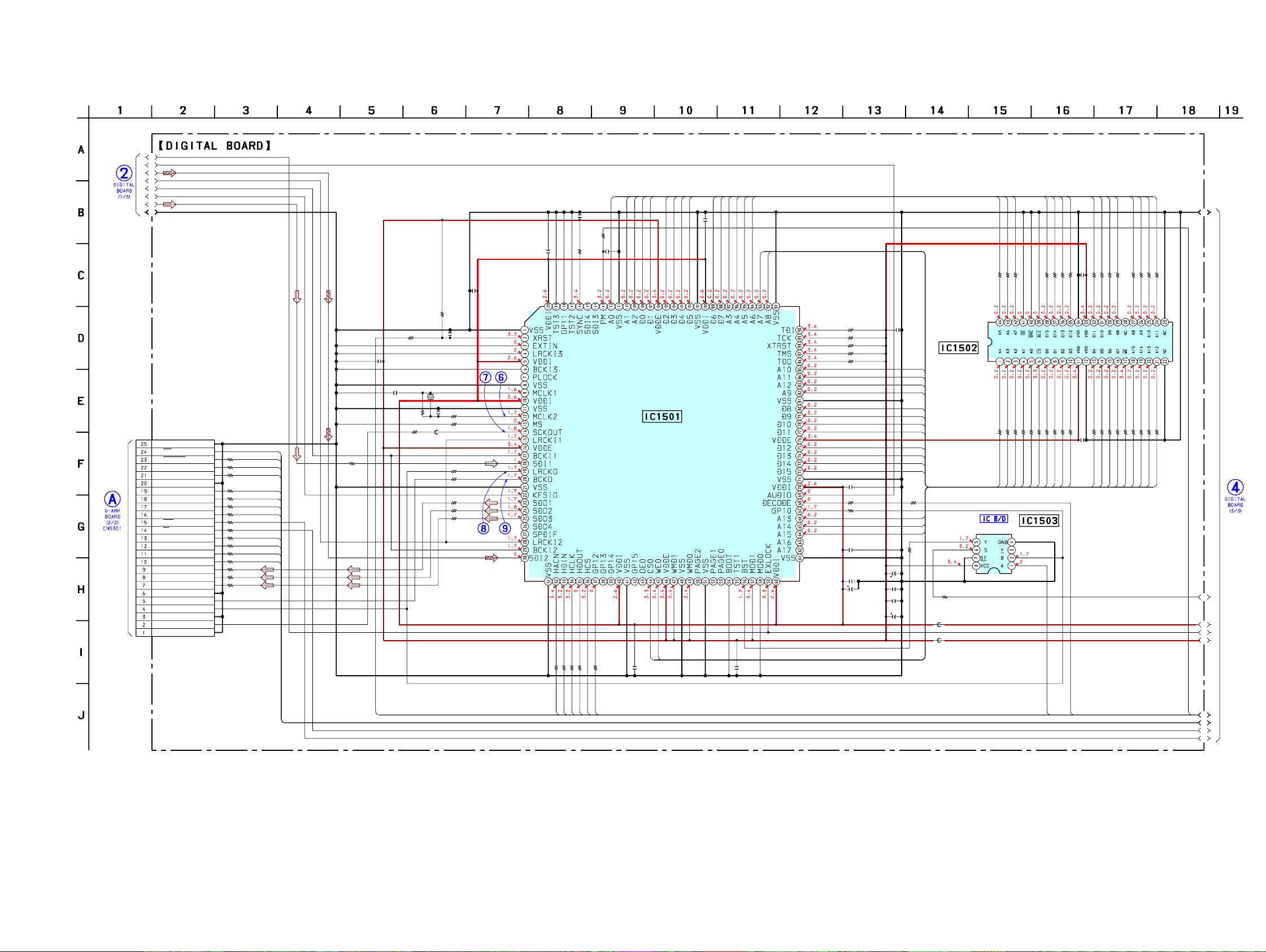
• See page 19 for Waveforms. • See page 29 for IC Block Diagrams. • See page 34 for IC Pin Function Description.
5-7. SCHEMATIC DIAGRAM – DIGITAL Board (2/3) –
R1532
R1533
R1545
R1546
R1548
R1549
R1550
R1551
R1502
R1191
R1192
R1195
R1181
R1182
R1183
R1184
R1185
R1187
R1188
R1171
R1172
R1173
R1170
R1166
R1174
JR1106
C1507
R1520
R1521
R1522
R1518
R1519
R1517
R1554
R
1553
R1552
R1525
R1526
C1519
R1534
R1547
R1541
R1535
R1536
R1537
R
1538
R1539
R1540
R1542
R1543
R1555
R1544
R1527
R1528
R1514
C1510
C1514
C1506
R1570
R1571
R1572
R1573
R1574
R1508
R1161
R1160
R1509
R1121
C1504 C1505
R1506
R1505
R1504
R1503
R1523
R1513
C1522
X1502
R1515
C1521
R1501 C1511
C1501
R1512
R1511
R1142
C1520
FB1501
FB1502
C1516
C1515
C1502
C1518
C1525
C1517
C1509
R1150
C1503
FB1503R1556
CNS1101
IC1502
IC1503
R1120
R1529
C1508
C1513
JR1104
IC1501
220
220
220
220
220
220
220
220
100
100
100
100
100
100
100
100
100
100
100
100
100
100
100
100
100
0
0.1
220
220
220
220
220
220
220
220
220
220
220
0.1
220
220
220
220
220
220
220
220
220
220
220
220
220
220
220
10k
0.1
0.1
0.1
10k
10k
10k
10k
10k
100
100
100
100
100
0.1 0.1
100
100
100
220
220
10k
10p
13.9MHz
1M
10p
100 0.1
0.1
1k
100
100
0.1
0.1
470
10V
0.1
0.1
100
16V
470
10V
0.1
100
0.1
100
25P
IS61LV6416-10TLT
TC7WH157FU
100
220
0.1
0.1
0
CXD9720BQ
B8
B1
B2
B3
B4
B5
B6
B7
C1
C2
C3
C4
C5
C6
C7
C8
C9
INT
SMUTE
SCDT
SHIFT
HDOUT
GP12
PM
XRST
HACN
HCS
BST
GP9
A7
A8
A13
A14
A15
A7
A8
A9
A10
A11
A12
A13
A14
A15
D8
D9
D10
D11
D12
D13
D14
D15
A10
A11
A12
A9
D8
D9
D10
D11
D12
D13
D14
D15
A0
A0
A1
A1
A2
A2
D0
D0
D1
D1
D2
D2
D3
D3
D4
D4
D5
D5
D6
D6
D7
D7
A3
A3
A4
A4
A5
A5
A6
CS0
CS0
WE0
WE0
A6
LAT1
LAT2
LAT3
OVFW
OVF
FON
FCTL
FCLK
HCLK
HDIN
D1
D2
D3
BCKO
LRCKO
DGND
SCDT
SHIFT
DGND
LAT1
LAT2
LAT3
INIT
REST
SD
DGND
SOFT MUTE
OVF
SCK
FAN-CLK
FAN ON/OFF
FAN-CTRL
DGND
OVFW
DGND
(2/3)
S-RAM
DIGITAL AUDIO
SIGNAL PROCESSOR
BOOT SELECT
(Page 16)
(Page 23)
(Page
18)
Loading...