


STR-DG700
Table of contents
 Loading...
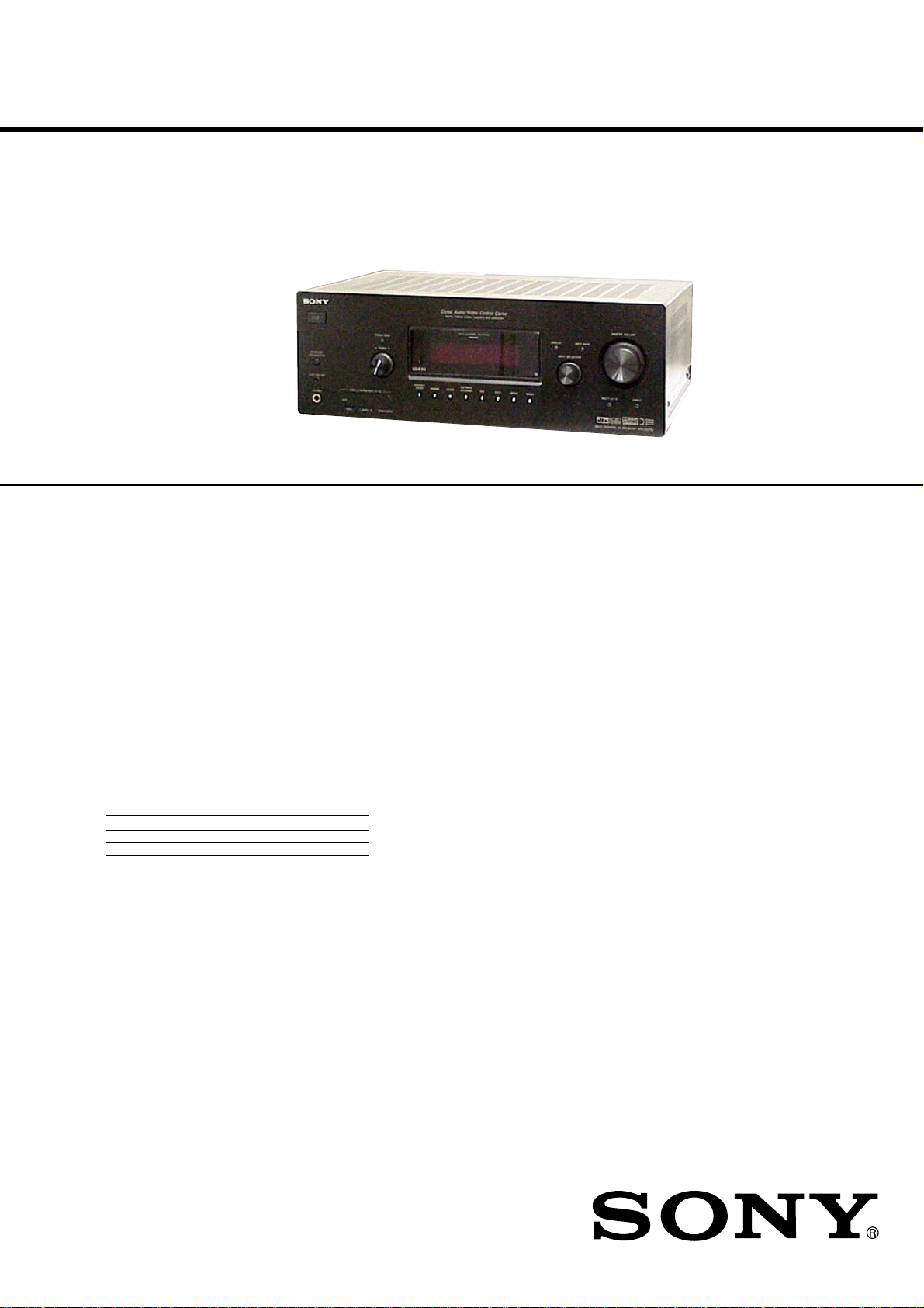
1
SERVICE MANUAL
AEP Model
UK Model
Australian Model
STR-DG700
MULTI CHANNEL AV RECEIVER
Amplifier section
Stereo Power Output
1)
, Reference Power Output
1) 2)
8 ohms 20 Hz – 20 kHz, THD 0.09 %
85 W + 85 W, 110 W/ch
8 ohms 1 kHz, THD 0.7 % 100 W + 100 W, 120 W/ch
8 ohms 1 kHz, THD 10 % 125 W + 125 W, 150 W/ch
1) Measured under the following conditions:
Area code Power requirements
AEP, UK 230 V AC, 50 Hz
AUS 240 V AC, 50 Hz
2) Reference power output for front, center, surround
and surround back. Depending on the sound field
settings and thjxsource, there may be no sound output.
Frequency response
Analog 10 Hz – 70 kHz
+0.5/–2 dB (with sound
field and equalizer bypassed)
SPECIFICATIONS
Inputs
Analog Sensiti vity: 500 mV/
50 kohms
S/N
3)
: 96 dB
(A, 500 mV
4)
)
Digital (Coaxial) Impedance: 75 ohms
S/N: 100 dB
(A, 20 kHz LPF)
Digital (Optical) S/N: 100 dB
(A, 20 kHz LPF)
Outputs (Analog)
AUDIO OUT Voltage: 500 mV/10 kohms
SUB WOOFER, SURROUND
Voltage: 2 V/1 kohm
Equalizer
Gain levels ±6 dB, 1 dB step
3) INPUT SHORT (with sound field and equalizer
bypassed).
4) Weighted network, input level.
Ver. 1.0 2006. 04
9-887-177-01
2006D04-1
© 2006. 04
Sony Corporation
Home Audio Division
Published by Sony Techno Create Corporation
Manufactured under license from Dolby Laboratories.
“Dolby”, “Pro Logic”, “Surround EX”, and the double-D
symbol are trademarks of Dolby Laboratories.
“DTS”, “DTS-ES”, “Neo:6”, and “DTS 96/24” are
trademarks of Digital Theater Systems, Inc.
This receiver incorporates High-Definition
Multimedia Interface (HDMI
TM
) technology. HDMI,
the HDMI logo and High-Definition Multimedia
Interface are trademarks or registered trademarks of
HDMI Licensing LLC.
– Continued on next page –
Photo: Black type
2
STR-DG700
FM tuner section
Tuning range 87.5 – 108.0 MHz
Intermediate frequency 10.7 MHz
Useable sensitivity 11.2 dBf, 1 µV/75 ohms
S/N
Mono/Stereo 76 dB/70 dB
Harmonic distortion at 1 kHz
Mono/Stereo 0.3%/0.5%
Separation 45 dB at 1 kHz
Frequency response 30 Hz – 15 kHz,
+0.5/–2 dB
AM tuner section
Tuning range
With 9-kHz tuning scale: 531 – 1,602 kHz
Intermediate frequency 450 kHz
Usable sensitivity 50 dB/m (at 1,000 kHz or
999 kHz)
Video section
Inputs/Outputs
Video: 1 Vp-p, 75 ohms
S-video: Y: 1 Vp-p, 75 ohms
C: 0.286 Vp-p, 75 ohms
COMPONENT VIDEO: Y: 1 Vp-p, 75 ohms
PB/CB/B-Y: 0.7 Vp-p/
75 ohms
PR/CR/R-Y: 0.7 Vp-p/
75 ohms
80 MHz HD Pass Through
General
Power requirements
Area code Power requirements
AEP, UK 230 V AC, 50/60 Hz
AUS 240 V AC, 50 Hz
Power consumption 220 W
Power consumption (during standby mode)
0.2 W
AC outlets 1 switched, 100 W/0.4 A MAX
Dimensions (w/h/d) (Approx.)
430 × 157.5 × 316 mm
including projecting parts and
controls
Mass (Approx.) 8.5 kg
Supplied accessories
FM wire antenna (1)
AM loop antenna (1)
Remote commander RM-AAP011 (1)
R6 (size-AA) batteries (2)
Optimizer microphone ECM-AC2 (1)
Design and specifications are subject to change
without notice.
•Abbreviation
AUS: Australian model
SAFETY-RELATED COMPONENT WARNING!!
COMPONENTS IDENTIFIED BY MARK 0 OR DOTTED LINE
WITH MARK 0 ON THE SCHEMATIC DIAGRAMS AND IN
THE PARTS LIST ARE CRITICAL TO SAFE OPERATION.
REPLACE THESE COMPONENTS WITH SONY P ARTS WHOSE
PART NUMBERS APPEAR AS SHOWN IN THIS MANUAL OR
IN SUPPLEMENTS PUBLISHED BY SONY.
MODEL IDENTIFICATION
— BACK PANEL —
Part No.
MODEL PART No.
AEP, UK 2-661-147-7s
AUS 2-661-147-8s
•Abbreviation
AUS: Australian model

3
STR-DG700
TABLE OF CONTENTS
1. GENERAL
Description and location of parts............................................. 4
2. DISASSEMBL Y
2-1. Case ..................................................................................... 7
2-2. Back Panel Section.............................................................. 8
2-3. Front Panel Section ............................................................. 8
2-4. DIGITAL Board .................................................................. 9
2-5. MAIN Board Section .......................................................... 9
2-6. STANDBY Board ............................................................. 10
2-7. REGULATOR Board ........................................................ 10
3. TEST MODE ..................................................................... 11
4. DIAGRAMS
4-1. Circuit Boards Location .................................................... 12
4-2. Block Diagram – Tuner/Audio Section –.......................... 13
4-3. Block Diagram – Digital Section – ................................... 14
4-4. Block Diagram – Video Section – .....................................15
4-5. Block Diagram – Key/Display/HDMI Section – .............. 16
4-6. Block Diagram – Power Section – .................................... 17
4-7. Printed Wiring Boards – Main Section – .......................... 19
4-8. Schematic Diagram – Main Section (1/3) – ...................... 20
4-9. Schematic Diagram – Main Section (2/3) – ...................... 21
4-10. Schematic Diagram – Main Section (3/3) – ...................... 22
4-11. Printed Wiring Board – Digital Section (1/2) – ................ 23
4-12. Printed Wiring Board – Digital Section (2/2) – ................ 24
4-13. Schematic Diagram – Digital Section (1/5) – ................... 25
4-14. Schematic Diagram – Digital Section (2/5) – ................... 26
4-15. Schematic Diagram – Digital Section (3/5) – ................... 27
4-16. Schematic Diagram – Digital Section (4/5) – ................... 28
4-17. Schematic Diagram – Digital Section (5/5) – ................... 29
4-18. Printed Wiring Boards
– Front B/Center/Surround Back Speaker Section – ........ 30
4-19. Schematic Diagram
– Front B/Center/Surround Back Speaker Section – ........ 31
4-20. Printed Wiring Board – Video Section (1/2) – .................. 32
4-21. Printed Wiring Board – Video Section (2/2) – .................. 33
4-22. Schematic Diagram – Video Section (1/2) – ..................... 34
4-23. Schematic Diagram – Video Section (2/2) – ..................... 35
4-24. Printed Wiring Boards
– S-video/Video3/REG Section – ..................................... 36
4-25. Schematic Diagram
– S-video/Video3/REG Section – ..................................... 37
4-26. Printed Wiring Board – HDMI Section – ..........................38
4-27. Schematic Diagram – HDMI Section – ............................ 39
4-28. Printed Wiring Board – ADCC Section – ......................... 40
4-29. Schematic Diagram – ADCC Section – ............................ 40
4-30. Printed Wiring Boards – Display Section – ...................... 41
4-31. Schematic Diagram – Display Section –........................... 42
4-32. Printed Wiring Boards – Power Section –.........................43
4-33. Schematic Diagram – Power Section – ............................. 44
5. EXPLODED VIEWS
5-1. Case Section ...................................................................... 58
5-2. Front Panel Section ........................................................... 59
5-3. Back Panel Section............................................................ 60
5-4. Chassis Section ................................................................. 61
6. ELECTRICAL PARTS LIST ........................................ 62
4
STR-DG700
SECTION 1
GENERAL
This section is extracted
from instruction manual.
4
GB
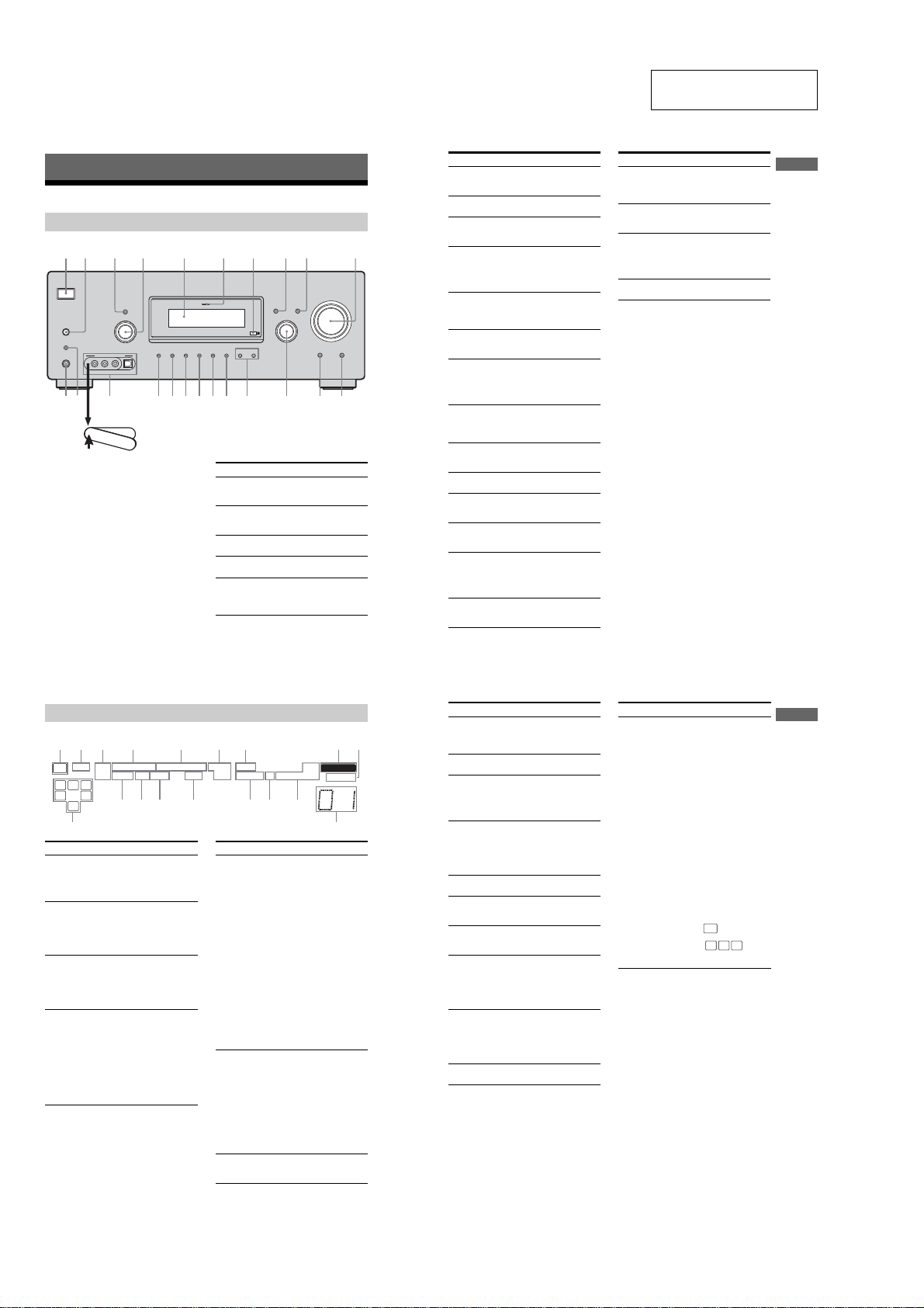
Description and location of parts
To remove t h e c over
Press PUSH.
When you remove the cover, keep it out of
reach from children.
Getting Started
Front panel
?/1
AUTO CAL MIC
SPEAKERS
(OFF/A/B/A+B)
PHONES
MEMORY/
ENTER
SUR BACK
DECODING 2CHSLEEPDIMMER A.F.D. MOVIE MUSIC
MULTI CHANNEL DECODING
TUNING MODE
DISPLAY INPUT MODE
INPUT SELECTOR
TUNING
–+
MULTI CH IN DIRECT
MASTER VOLUME
VIDEO 3 IN/PORTABLE AV IN
VIDEO L AUDIO R DIGITAL(OPT)
P
U
S
H
15268q
;
4397
qaqswd qdqfwaws qgqhqjqkqlw;
Name Function
A ?/1 Press to turn the receiver
on or off (page 29, 36, 37,
57, 59).
B SPEAKERS
(OFF/A/B/A+B)
Press to select OFF, A, B,
A+B of the front speakers
(page 30).
C TUNING MODE Press to select the tuning
mode (page 58, 62).
D TUNING +/– Turn to scan a station
(page 58, 61).
E Display The current status of the
selected component or a
list of selectable items
appears here (page 6).
5
GB
Getting Started
Name Function
F MULTI CHANNEL
DECODING lamp
Lights up when multi
channel audio is decoded
(page 37).
G Remote sensor Receives signals from
remote commander.
H DISPLAY Press to select information
displayed on the display
(page 63, 67).
I INPUT MODE Press to select the input
mode when the same
components are connected
to both digital and analog
jacks (page 64).
J MASTER
VOLUME
Turn to adjust the volume
level of all speakers at the
same time (page 34, 35,
36, 37).
K DIRECT Press to listen to high
quality analog sound
(page 56).
L MULTI CH IN Press to select the audio
directly from the
components connected to
the MULTI CH IN jacks
(page 35).
M INPUT
SELECTOR
Turn to s e lect the input
source to playback (page
35, 36, 37, 56, 58, 62, 64,
67, 68, 69).
N MOVIE,
MUSIC
Press to select sound fields
(MOVIE, MUSIC) (page
53).
O A.F.D. Press to select A.F.D.
mode (page 51).
P 2CH Press to select 2CH
STEREO mode (page 56,
57).
Q SUR BACK
DECODING
Press to select the
surround back decoding
mode (page 44).
R SLEEP Press to activate the Sleep
Timer function and the
duration which the
receiver turns off
automatically (page 68).
S DIMMER Press to change the
brightness of the display
(page 50).
Name Function
T MEMORY/ENTER Press to store a station or
enter the selection when
selecting the settings
(page 29, 60).
U VIDEO 3 IN/
PORTA BLE A V IN
jacks
To c onnect a camcorder or
video game (page 27, 35).
V AUTO CAL MIC
jack
Connects to the supplied
ECM-AC2 optimizer
microphone for the Auto
Calibration function (page
31).
W PHONES jack Connects to a headphone
(page 77).
6
GB
About the indicators on the display
MEMORY
L C R
SL
S
SR
SB
SW
LFE
SP A
SP B
RDS
STEREO MONO
A.DIRECT
D.RANGE EQ
NEO:6
SLEEP OPT COAX HDMI 96/24
DIGITAL EX
;
DTS-ES
;
PRO LOGIC IIx
qd qs qa
qj
qk
qgqh
qf
2143567 89
q;
Name Function
A SW Lights up when sub wo of er
selection is set to “YES” (page
41) and the audio signal is
output from the SUB WOOFER
jack.
B LFE Lights up when the disc being
played back contains an LFE
(Low Frequency Effect)
channel and the LFE channel
signal is actually being
reproduced.
C SP A/SP B Lights up according to the
speaker system used. However,
these indicators do not light up
if the speaker output is turned
off or if a headphone is
connected.
D ;DIGITAL
(EX)
Lights up when Dolby Digital
signals are input. “;
DIGITAL EX” lights up when
Dolby Digital Surround EX
signals are decoded.
Note
When playing a Dolby Digital
format disc, be sure that you
have made digital conn e ctions
and that INPUT MODE is not
set to “ANALOG” (page 64).
Name Function
E ;PRO
LOGIC (II)/
(IIx)
Lights up when the receiver
applies Pro Logic processing to
2 channel signals in order to
output the center and surround
channel signals. “; PRO
LOGIC II” lights up when the
Pro Logic II Movie/Music/
Game decoder is activated.
“; PRO LOGIC IIx” lights up
when the Pro Logic IIx Movie/
Music/Game decoder is
activated. However, these
indicators do not light up if both
the center and surround
speakers are set to “NO” (page
41) and you select a sound field
using the A.F.D. button.
Note
Dolby Pro Logic IIx decoding
does not function for DTS
format signals or for signals
with a sampling frequency of
more than 48 kHz.
F DTS (-ES)/
(96/24)
Lights up when DTS signals are
input. “DTS-ES” lights up
when DTS-ES signals are input.
“DTS 96/24” lights up when the
receiver is decoding DTS 96
kHz/24 bit signals.
Note
When playing a DTS format
disc, be sure that you have made
digital connections and that
INPUT MODE is not set to
“ANA LO G” (page 64).
G NEO:6 Lights up when DTS Neo:6
Cinema/Music decoder is
activated (page 52).
7
GB
Getting Started
Name Function
H MEMORY Lights up when a memory
function, such as Preset
Memory (page 61), etc., is
activated.
I A.DIRECT Lights up when ANALOG
DIRECT is selected (page 56).
J Preset
station
indicators
Lights up when using the
receiver to tune in radio stations
you have preset. For details on
presetting radio stations, see
page 60.
K Tuner
indicators
Lights up when using the
receiver to tune in radio stations
(page 57), etc.
Note
“RDS” appears for models of
area code CEL, CEK only.
L EQ Lights up when the equalizer is
activated (page 39).
M D.RANGE Lights up when dynamic range
compression is activated (page
39).
N HDMI Flashes when you select
“HDMI A.” in the VIDEO
menu (page 66).
O COAX Lights up when INPUT MODE
is set to “AUTO” and the source
signal is a digital signal being
input through the COAXIAL
jack, or when INPUT MODE is
set to “COAX IN” (page 64).
P OPT Lights up when INPUT MODE
is set to “AUTO” and the source
signal is a digital signal being
input through the OPTICAL
jack, or when INPUT MODE is
set to “OPT IN” (page 64).
Q SLEEP Lights up when the sleep timer
is activated (page 68).
Name Function
R Playback
channel
indicators
L
R
C
SL
SR
S
SB
The letters (L, C, R, etc.)
indicate the channels being
played back. The boxes around
the letters vary to show ho w the
receiver downmixes the source
sound (based on the speaker
settings).
Front Left
Front Right
Center (monaural)
Surround Left
Surround Right
Surround (monaural or the
surround components obtained
by Pro Logic processing)
Surround back (the surround
back components obtained by
6.1 channel decoding)
Example:
Recording format (Front/
Surround): 3/2.1
Output channe l: When surroun d
speaker is set to “NO” (page 41)
Sound Field: A.F.D. AUTO
L C R
SL SR
SW
5
STR-DG700
8
GB
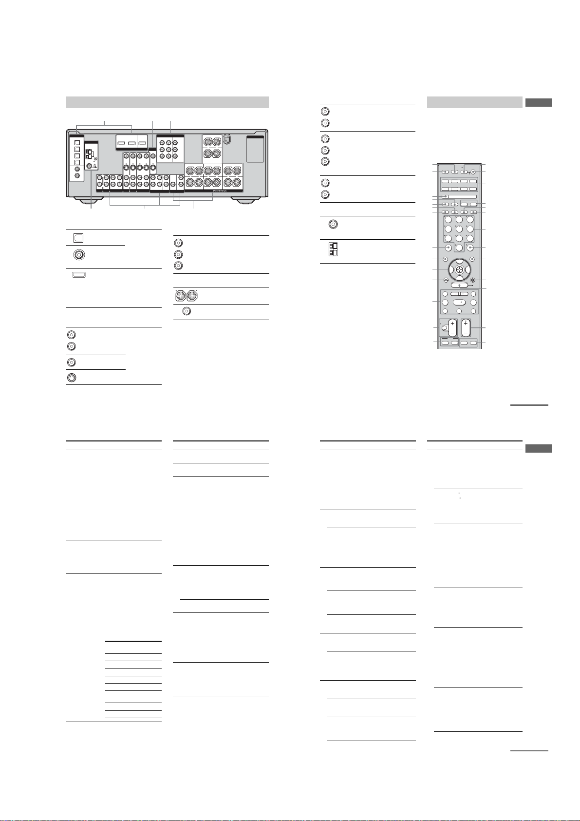
Rear panel
AC OUTLET
DIGITAL
VIDEO 1
IN
VIDEO 2
IN
MD/
TAPE
IN
MD/
TAPE
OUT
DVD
IN
SA-CD/
CD
IN
COAXIAL
OPTICAL
ANTENNA
AM
HDMI
DVD IN
ASSIGNABLE
VIDEO 2 IN
MONITOR OUT
L
R
AUDIO IN
VIDEO IN
DVD
AUDIO IN
S-VIDEO
IN
VIDEO IN
VIDEO 2
AUDIO IN
S-VIDEO
IN
VIDEO OUT
VIDEO 1
AUDIO OUT
S-VIDEO
OUT
VIDEO IN
S-VIDEO
IN
L
R
SA-CD
/
CD
MD/TAPE
OUT
L
R
IN
IN
AUX
IN
L
R
VIDEO OUT
S-VIDEO
OUT
MONITOR
SURROUND BACK
CENTER
+
–
SURROUND FRONT A
R
R
L
L
+
–
+
–
SPEAKERS
FRONT B
R
L
+
–
SUB
WOOFER
SURROUND
PRE OUT
L
R
SURROUND
SUB
WOOFER
CENTER
FRONT
L
R
MULTI CH IN
DVD
IN
VIDEO 2
IN
MONITOR
OUT
COMPONENT VIDEO
Y
ASSIGNABLE
P
B
/C
B
/BñY
P
R
/C
R
/RñY
23
4
6 5
1
A DIGITAL INPUT/OUTPUT section
OPTICAL
IN/OUT jack
Connects to a DVD
player, etc. The
COAXIAL jack
provides a better
quality of loud
sound (page 16, 23,
25).
COAXIAL IN
jack
HDMI IN/
MONITOR
OUT jack*
Connects to a DVD
player, or a satellite
tuner. The image
and the sound are
output to a TV or a
projector (page
26).
B VIDEO/AUDIO INPUT/OUTPUT
section
AUDIO IN/
OUT jack
Connects the video
and audio jacks of
a VCR or a DVD
player (page 22,
23, 24, 25, 27).
VIDEO IN/
OUT jack*
S-VIDEO IN/
OUT jack*
White (L)
Red (R)
Yellow
C COMPONENT VIDEO INPUT/
OUTPUT section
COMPONENT
VIDEO
INPUT/
OUTPUT
jack*
Connects to a DVD
player, TV, or a
satellite tuner. You
can enjoy high
quality image
(page 22, 24, 25).
D SPEAKER section
Connects to
speakers (page 14).
Connects to sub
woofer (page 14).
Green
Blue
Red
9
GB
Getting Started
*You can watch the selected input image when you
connect the MONITOR OUT jack to a TV monitor
(page 22).
You can use the supplied remote RM-AAP011
to operate the receiver and to control the Sony
audio/video components that the remote is
assigned to operate. You can also program the
remote to control non-Sony audio/video
components. For details, see “Programming
the remote” (page 69).
E AUDIO INPUT/OUTPUT section
AUDI O IN/
OUT jack
Connects to an MD
deck or CD player,
etc. (page 19).
MULTI
CHANNEL
INPUT jack
Connects to a
Super Audio CD
player or DVD
player which has
an analog audio
jack for 5.1
channel sound
(page 18).
PRE OUT jack Connects to an
external power
amplifier.
F ANTENNA section
FM
ANTENNA
Connects to the
FM wire antenna
supplied with this
receiver (page 28).
AM
ANTENNA
Connects to the
AM loop antenna
supplied with this
receiver (page 28).
White (L)
Red (R)
White (L)
Red (R)
Black
White (L)
Red (R)
Remote commander
SYSTEM STANDBY
TUNING –
DISC SKIP
MUTING
TOP MENU
MENU F1
TV/VIDEO WIDE
F2
TV VOL
MASTER VOL
TV CH
PRESET
TUNING +
DISPLAY TOOLS
RETURN/
EXIT
AMP
REPLAY ADVANCE
AV ?/1
TV
VIDEO 1 VIDEO 2 DVDVIDEO 3
MD/TAPE SA-CD/CD
AUX
MULTI CH
2CH A.F.D. MOVIE MUSIC
SLEEP
FM MODE D. TUNING AUTO CAL
TUNER
RM SET UP
?/1
MEMORY
.
>
m M
xX
B
B
V
v
MENU
H
3
CLEAR
>10
–
/
–
–
<
<
DVD
12
45
78
6
9
ENTER
0/10
1
3
2
wj
qs
qd
9
q;
qa
7
6
4
wg
wh
AV ?/1
(on/standby) switch
?/1
(on/standby)
switch
qf
qg
qj
qk
ws
wa
wd
wf
5
8
qh
ql
w;
continued
10
GB
Name Function
A AV ?/1 Press to turn on or off the
audio/video components that
the remote is programme d to
operate.
To turn the TV on or off, press
TV (Z) and then press AV
?/1.
If you press ?/1 (B) at the
same time, it will turn off the
receiver and other
components (SYSTEM
STANDBY).
Note
The function of the AV ?/1
switch changes automatically
each time you press the input
buttons (C).
B ?/1 Press to turn the receiver on or
off.
To t urn off all compo nents,
press ?/1 and A V ?/1 (A) at
the same time (SYSTEM
STANDBY).
C Input buttons Press one of the buttons to
select the component you
want to use. When you press
any of the input buttons, the
receiver turns on. The buttons
are factory assigned to control
Sony components as follows.
You can program the remote
to control non-Sony
components following the
steps in “Programming the
remote” on page 69.
D MOVIE,
MUSIC
Press to select sound fields
(MOVIE, MUSIC).
Button Assigned Sony
component
VIDEO 1 VCR (VTR mode 3)
VIDEO 2 VCR (VTR mode 2)
VIDEO 3 VCR (VTR mode 1)
DVDDVD player
MD/TAPE MD deck
SA-CD/CD Super Audio CD/CD
player
TUNER Built-in tuner
AUXNot assigned
Name Function
E D. TUNING Press to enter direct tuning
mode.
F AUTO CAL Press to activate the Auto
Calibration function.
G Numeric
buttons
(number 5
a)
)
Press to
–preset/tune to preset
stations.
–select track numbers of the
CD player, VCD player, LD
player, DVD player, MD
deck, DAT deck, or tape
deck. Press 0/10 to select
track number 10.
–select channel numbers of
the VCR, satellite tuner,
Blu-ray disc recorder, PSX,
DVD/VIDEO COMBO, or
DVD/HDD COMBO.
Press TV (Z) and then press
the numeric buttons to select
the TV channels.
H ENTER Press to enter the value after
selecting a channel, disc or
track using the numeric
buttons. To enter the value of
Sony TV, press TV (Z) and
then press ENTER.
MEMORY Press MEMORY to store a
station.
I TOOLS Press to display options
applicable to the entire disc
(e.g. disc protection), recorder
(e.g. audio settings during
recording), or multiple items
on a list menu (e.g. erasing
multiple titles). To display the
options of Sony TV, press TV
(Z) and then press TOOLS.
J AMP Press AMP to light up the
button and then press MENU
(K) to display the menu of
the receiver. Then, use the
control buttons to perform
menu operations.
11
GB
Getting Started
Name Function
K MENU Press to display the menus of
the VCR, DVD player,
satellite tuner, Blu -r ay disc
recorder, PSX, DVD/VIDEO
COMBO, or DVD/HDD
COMBO on the TV screen.
Then, use the control buttons
to perform menu operations.
To display the menus of Sony
TV, press TV (Z) and then
press MENU.
L TV CH +
a)
/– Press TV (Z) and then press
TV CH +/– to select preset TV
channels.
PRESET
+
a)
/–
Press to
–select preset stations.
–select preset channels of the
VCR, satellite tuner, Blu-ray
disc recorder, DVD player,
DVD/VIDEO COMBO, or
DVD/H DD COMBO.
M F1 , F2 Press to select the media (for
DVD/VIDEO COMBO and
DVD/HDD COMBO models
only).
TV/VIDEO Press TV (Z) and then press
TV/VIDEO to select the input
signal (TV input or video
input).
WIDE Press TV (Z) and then press
WIDE to select the wide
picture mode.
N DVD TOP
MENU
Press to display DVD title.
Then, use the control buttons
to perform menu operations.
DVD MENU Press to display the menu of
the DVD player on the TV
screen. Then, use the control
buttons to perform menu
operations.
O TV VOL +/– Press TV (Z) and then press
TV VOL +/– to adjust the TV
volume level.
MASTER
VOL + /–
Press to adjust the volume
level of all speakers at the
same time.
MUTING Press to mute the sound.
To mute the sound of the TV,
press TV (Z) and then press
MUTING.
Name Function
P . /> Press to skip tracks of the
VCR, CD player, VCD player,
LD player, DVD player, MD
deck, DAT deck, tape deck,
Blu-ray disc recorder, PSX,
DVD/VIDEO COM BO, or
DVD/HDD COMBO.
REPLAY /
ADVANCE
Press to replay the previous
scene or fast forward the
current scene of the VCR,
DVD player, DVD/VIDEO
COMBO, or DVD/HDD
COMBO.
m/M Press to
–search tracks in the forward/
backward direction of the
CD player, VCD player,
DVD player, LD player , MD
deck, Blu-ray disc recorder,
PSX, DVD/VIDEO
COMBO, or DVD/HDD
COMBO.
–fast forward/rewind of the
VCR, DAT deck, or tape
deck.
H
a)
Press to start playback of the
VCR, CD player, VCD player,
LD player, DVD player, MD
deck, DAT deck, tape deck,
Blu-ray disc recorder, PSX,
DVD/VIDEO COMBO, or
DVD/H DD COMBO.
X Press to pause playback or
recording of the VCR, CD
player, VCD player, LD
player, DVD player, MD
deck, DAT deck, tape deck,
Blu-ray disc recorder, PSX,
DVD/VIDEO COMBO, or
DVD/HDD COMBO. (Also
starts recording with
components in recording
standby.)
x Press to stop playback of the
VCR, CD player, VCD
player, LD player, DVD
player, MD deck, DAT deck,
tape deck, Blu-ray disc
recorder, PSX, DVD/VIDEO
COMBO, or DVD/HDD
COMBO.
<
<
continued

6
STR-DG700
12
GB
a)
The number 5, TV CH +, PRESET + and H
buttons have tactile dots. Use the tactile dots as
references when operating the receiver.
Notes
•Some functions explained in this section may not
work depending on the mod el .
•The above explanation is intended to serve as an
example on ly. Therefore, d epending on the
component, the above operation may not be
possible or may operate differently than described.
Name Function
TUNING +/– Press to scan a station.
DISC SKIP Press to skip disc of the CD
player, VCD player, DVD
player, MD deck, or LD
player (multi-disc changer
only).
Q RETURN/
EXIT O
Press to
–return to the previous menu.
–exit the menu while the
menu or on-screen guide of
the VCD player, LD player,
DVD player, Blu-ray disc
recorder, PSX, or satellite
tuner is displayed on the TV
screen.
To return to the previous menu
of Sony TV, press TV (Z)
and then press RETURN/
EXIT O.
R Control
buttons
After pressing AMP (J),
then MENU (K) for receiver
operation, or DVD TOP
MENU (N), or DVD MENU
(N), press the control button
V, v, B or b to select the
settings. When you press
DVD TOP MENU or DVD
MENU, press the control
button to enter the select ion.
S DISPLAY Press to select information
displayed on the TV screen of
the VCR, VCD player, LD
player, DVD player, CD
player, MD deck, Blu-ray disc
recorder, PSX, satellite tuner,
DVD/VIDEO COMBO, or
DVD/HDD COMBO.
To select information of Sony
TV, press TV (Z) and then
press DISPLAY.
T CLEAR Press to
–clear a mistake when you
press the incorrect numeri c
button.
–return to continuous
playback, etc. of the Blu-ray
disc recorder, PSX, satellite
tuner, DVD/VIDEO
COMBO, or DVD/HDD
COMBO.
Name Function
-/-- Press to select the channel
entry mode, either one or two
digit of the Blu-ray disc
recorder, or satellite tuner.
To s elec t the channel entry
mode of the TV, press TV
(Z) and then press -/--.
>10 Press to select track numbers
over 10 of the CD player,
VCD player, LD player, MD
deck, tape deck, TV, VCR,
Blu-ray disc recorder, PSX, or
satellite tuner.
U SLEEP Press to activate the Sleep
Timer function and the
duration which the receiver
turns off automatically.
V FM MODE Press to select FM monaural
or stereo reception.
W 2CH Press to select 2CH STEREO
mode.
X A.F.D. Press to select A.F.D. mode.
Y MULTI CH Press to select the audio
directly from the components
connected to the MULTI CH
IN jacks.
Z TV Press to light up the button. It
changes the remote key
function to activate the
buttons with orange printing.
It also activate the TOOLS
(I), MENU (K),
RETURN/EXIT O (Q),
Control buttons (R) and
DISPLAY (S) buttons to
perform menu operations for
Sony TVs only.
wj RM SET UP Press to set up the remote.
7
STR-DG700
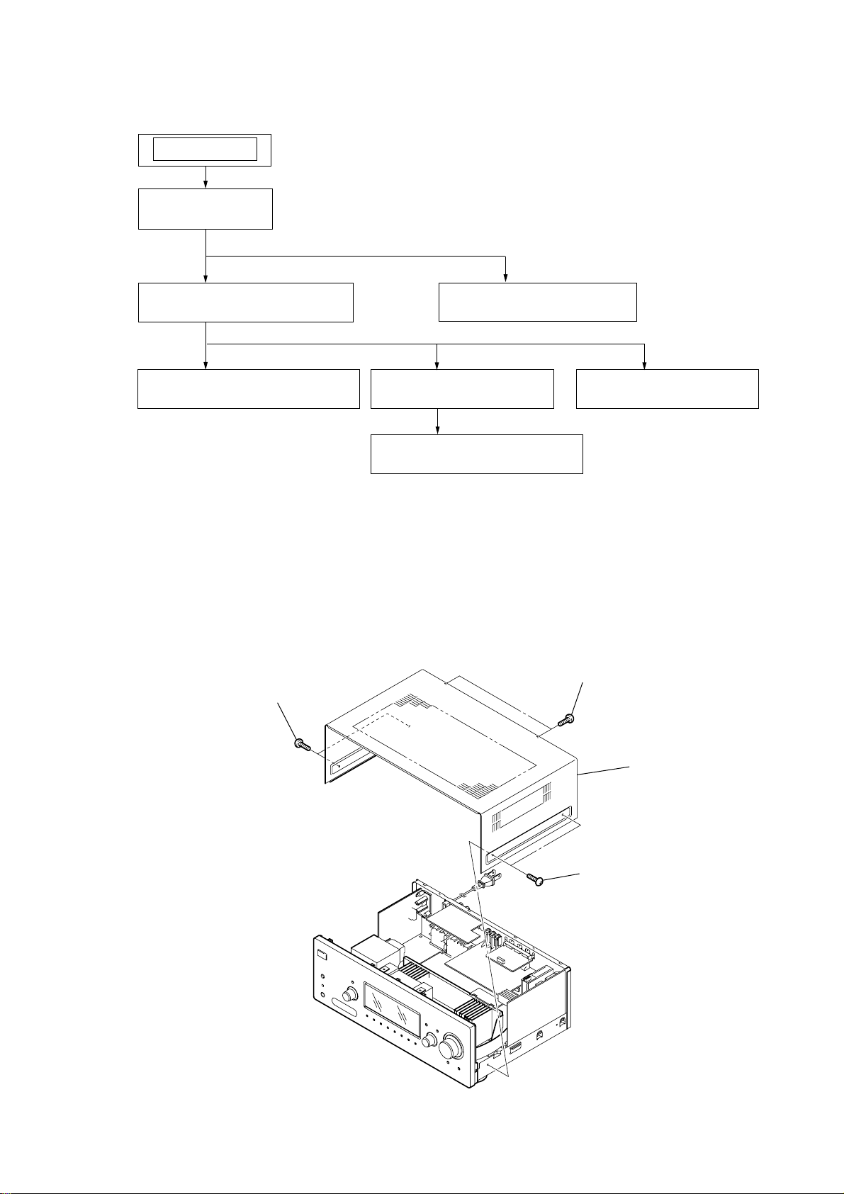
Note : This set can be disassemble according to the following sequence.
SECTION 2
DISASSEMBLY
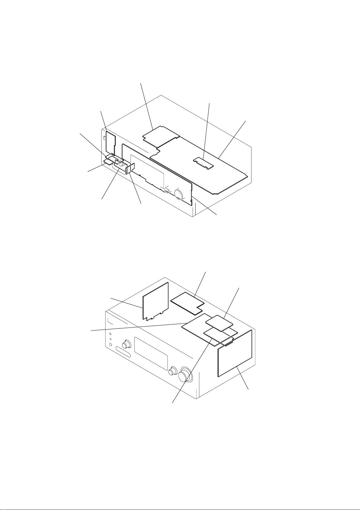
2-1. CASE
2-1. CASE
(Page 7)
2-2. BACK PANEL SECTION
(Page 8)
2-3. FRONT PANEL SECTION
(Page 8)
SET
2-6. STANDBY BOARD
(Page 10)
2-4. DIGITAL BOARD
(Page 9)
2-7. REGULATOR BOARD
(Page 10)
2-5. MAIN BOARD SECTION
(Page 9)
Note : Follow the disassembly procedure in the numerical order given.
1
two
screws
(case 3 TP2)
2
two
screws
(case 3 TP2)
3
two
screws
(+BVTP 3
×
8)
4
case
8
STR-DG700
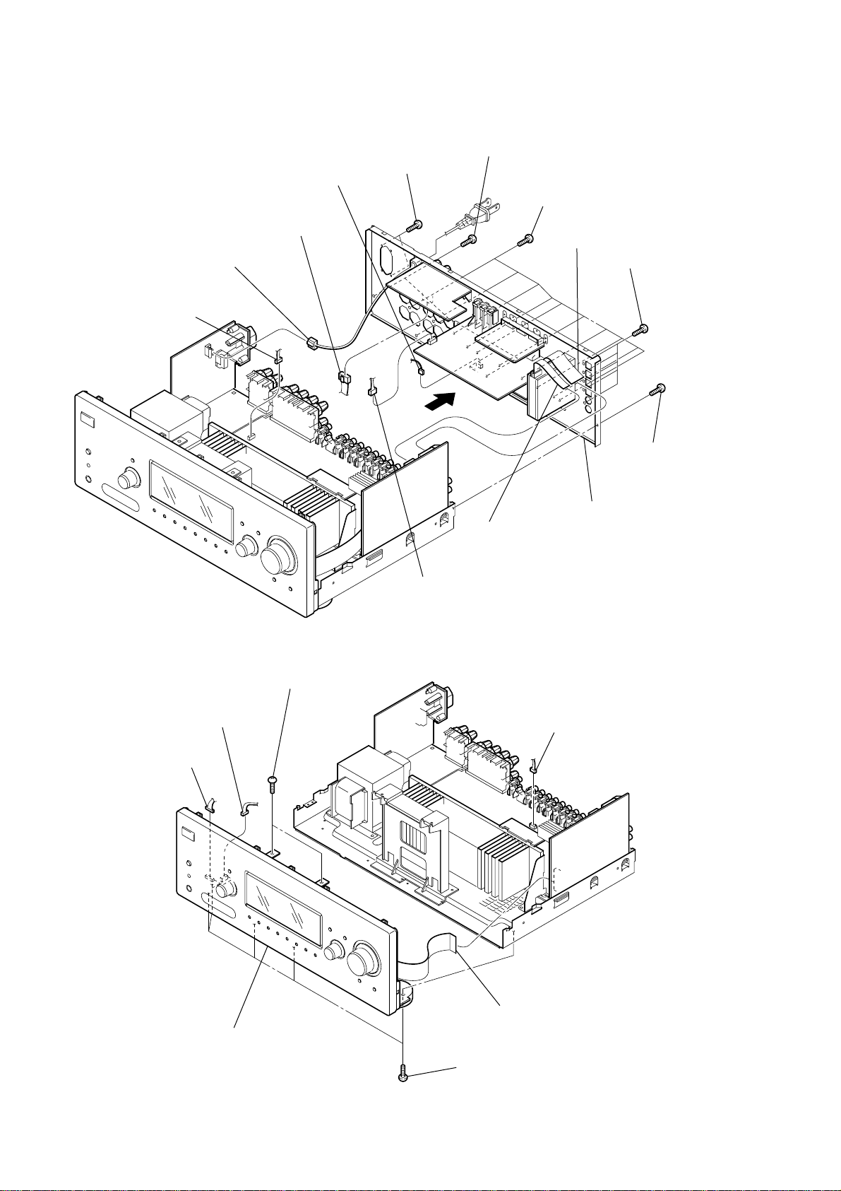
2-3. FRONT PANEL SECTION
2-2. BACK PANEL SECTION
9
two
screws
(+BVTP 3
×
8)
7
three
screws
(+BVTP 3
×
8)
0
ten
screws
(+BVTP 3
×
8)
qa
five
screws
(+BVTP 3
×
8)
8
screw
(+BVTP 3
×
8
)
qf
back panel section
5
CNS509 (21 core)
6
CNS508 (11 core) (AUS)
CNS508 (15 core) (AEP,UK)
1
CNP901 (2P)
2
CNP806 (3P)
3
CNP503 (4P)
qd
CNP2101 (3P)
4
CN302 (4P)
qs
6
five
screws
(+BVTP 3
×
8)
5
two
screws
(+BVTP 3
×
8)
7
front panel section
3
CNS505 (23 core)
1
CNP2000 (4P)
2
CNP791 (4P)
4
CNP503 (3P)
9
STR-DG700
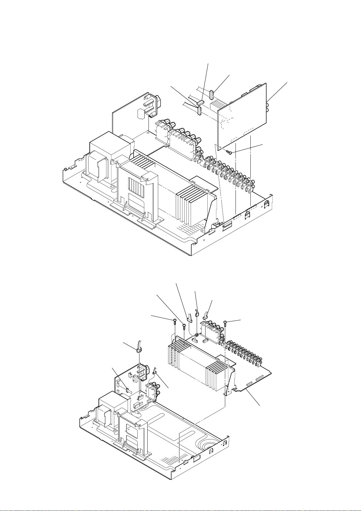
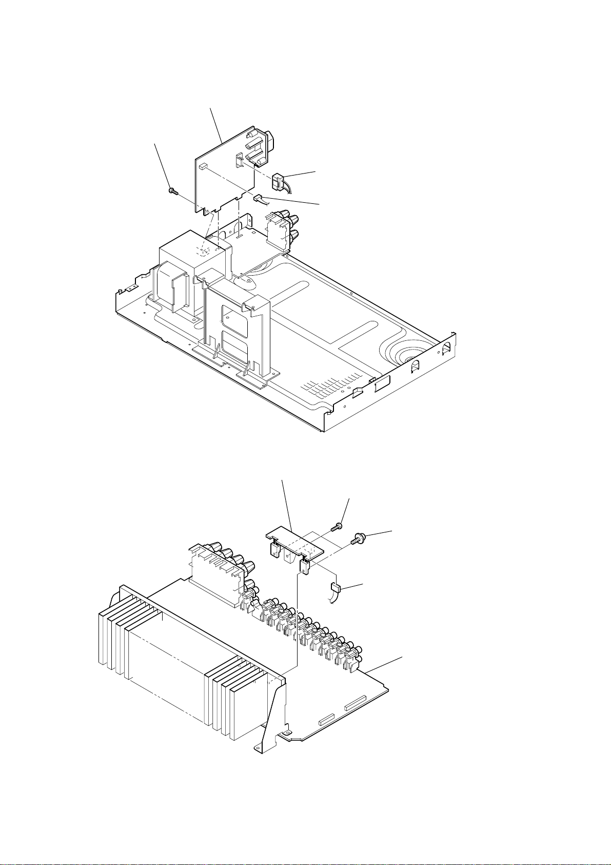
2-4. DIGIT AL BOARD
2-5. MAIN BOARD SECTION
4
screw
(+BVTP 3
×
8)
5
DIGITAL boar
d
1
CNP505 (10P)
2
CNP503 (5P)
3
CNP504 (7P)
2
CNP601 (4P)
1
CNP600 (5P)
4
CNP912 (3P)
5
CNP801 (3P)
6
CNP802 (5P)
3
CNP801 (5P)
7
two
screws
(+BV3 (3
-CR)
)
8
two
screws
(+BV3 (3
-CR)
)
9
screw
(+BV3 (3
-CR)
)
0
MAIN board section
10
STR-DG700
2-6. STANDBY BOARD
2-7. REGULATOR BOARD
4
STANDBY board
1
CNP902 (2P)
2
CNP804 (3P)
3
screw
(+BVTP 3
×
8)
2
screw
(+BVTP 3
×
8)
3
two
screws
(transister)
4
REGULATOR board
1
CN3013 (3P)
MAIN board section
11
STR-DG700
SECTION 3
TEST MODE
FACTORY PRESET MODE
* All preset contents are reset to the default setting.
* Procedure:
While depressing the [SPEAKERS $OFF/A/B/A+B%] and the
[MOVIE] buttons simultaneously, press the
?/1 button to turn
on the main power.
The message “FA CT OR Y” appears for a moment and the present
contents are reset to the default values.
VACUUM FLUORESCENT DISPLAY TEST MODE
* All fluorescent segments are tested.
When this test is activated, all segments light on at the same
time, then each segment lights on one after another.
* Procedure:
While depressing the [TUNING MODE] and the [DISPLAY] but-
tons simultaneously, press the ?/1 button to turn on the main
power.
1. ALL segments light on.
[MULTI CHANNEL DECODING] LED light on.
2. Turn the [INPUT SELECTOR] control, confirm display.
3. Turn the [INPUT SELECTOR] control, confirm display.
[MULTI CHANNEL DECODING] LED light on.
4. Turn the [INPUT SELECTOR] control, all segments and all LEDs
light off.
SOUND FIELD CLEAR MODE
* The preset sound field is cleared when this mode is activated.
Use this mode before returning the product to clients upon
completion of repair.
* Procedure:
While depressing the [2CH] button, press the ?/1 button to turn
on the main power.
The message “S.F. CLR.” appears for a moment and initializa-
tion is performed.
SOFTWARE VERSION DISPLAY MODE
* The software version is displayed.
* Procedure:
While depressing the [SPEAKERS $OFF/A/B/A+B%] and the
[DISPLAY] buttons simultaneously, press the ?/1 button to turn
on the main power.
The model name, destination and the software version are dis-
played for a moment.
KEY CHECK MODE
* Button check
* Procedure:
While depressing the [SPEAKERS $OFF/A/B/A+B%] and the [2CH]
buttons simultaneously , press the
?/1 button to turn on the main
power.
Either the message “REST 14” appears.
Every pressing of any button other than the
?/1 counts down
the buttons. The buttons which are already counted once are not
counted again. When all buttons are pr essed “REST 00” appears.
AUTOBETICAL MODE (AEP, UK model only)
* When this mode is used, the receiver scans the broadcasts that
can be received by the tuner, and sets up the broadcasts.
Be sure to start scanning after connecting the antenna.
* Procedure:
Check that the antenna is connected.
While depressing the [MEMORY/ENTER] button, press the ?/1
button to turn on the main power.
The message “AUTO-BETICAL SELECT” appears for a mo-
ment and the receiver starts scanning.
COMMAND MODE SELECTION MODE
* The command mode (AV1 or AV2) of the remote commander
can be selected.
* Procedure:
While depressing the [INPUT MODE] button, press the ?/1 but-
ton to turn on the main power.
Either the message “C.MODE.AV 1” or “C.MODE.AV 2” ap-
pears for a moment and select the desired mode.
L
SW
LFE
CR
SL S SR
SBL SB SBR
SP A
SP B SLEEP OPT COAX HDMI 96/24
DIGITALEX PRO LOGIC II x DTS-ES NEO:6 AAC CAT RDS
D.RANGE EQ STEREO MONO
A.DIRECT
D
D
D
D
dB
k Hz
m ft.
MHz
MEMORY
L
SW
LFE
R
S
SB
A
SLEEP COAX 96/24
EX DTSII NEO:6
D.RANGE
STEREO
dB
Hz
ft.
MEMORY
AAC
C
SL SR
SBL SBR
SP
SP B OPT HDMI
DIGITAL xPRO LOGIC -ES RDS
EQ MONO
A.DIRECT
D
D
D
D
k
m
MHz
CAT
12
STR-DG700
4-1. CIRCUIT BOARDS LOCATION
MAIN board
DISPLAY board
POWER board
ADCC board
HEADPHONE board
VIDEO3 board
OPT3 board
REGULATOR board
SPEAKER B board
STANDBY board
SPEAKER C/SB board
HDMI SW board
VIDEO board
DIGITAL boar
d
S-VIDEO board
SECTION 4
DIAGRAMS

STR-DG700
13 13
STR-DG700
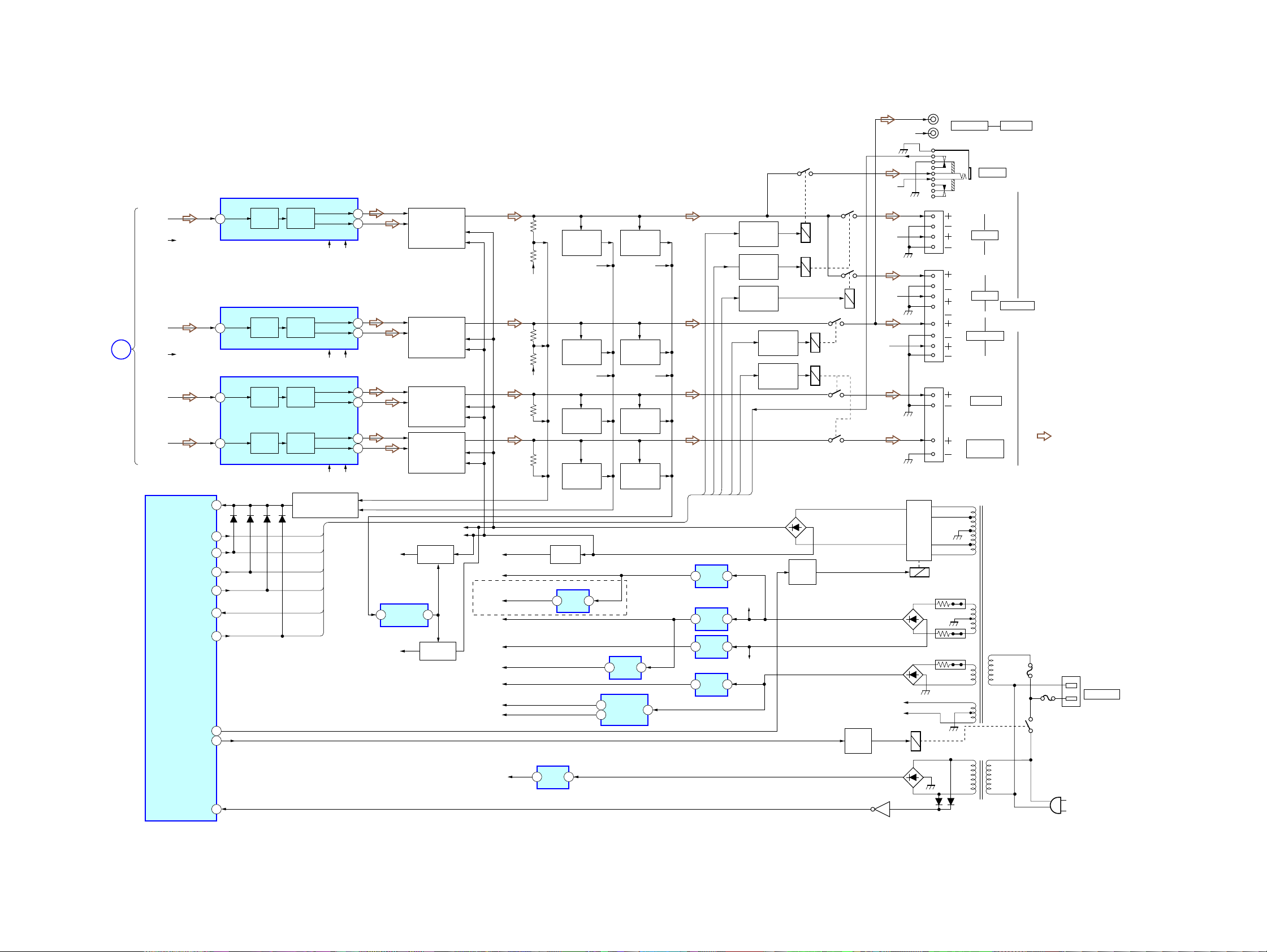
4-2. BLOCK DIAGRAM — TUNER/AUDIO SECTION —
43
76
75
78
74
73
70
SA-CD/CD
IN
MD/TAPE
OUT
MD/TAPE
IN
DVD AUDIO
IN
VIDEO 3 IN/
PORTABLE AV IN
L
J400
J403 J298(2/2) J404
R
R–CH
R–CH
R–CH
R–CH
LR
AM
TN1
FM/AM TUNER UNIT
SYSTEM CONTROL
IC1101 (1/5)
LRLR
L
-3 -4 -1 -2
-5 -6
RL
VIDEO 2
AUDIO OUT AUDIO INAUDIO IN
RLR
R–CH
RDS SIG
S LATCH
SW RY
VOL DA
VOL CL
STEREO
TUNED
MUTE
DO
17
TUNER DATA/FL DATA
16
T.SERIAL CLK/FL CLK
L–CH
AEP,UK MODEL
AEP,UK MODEL
AUS MODEL
R–CH
STEREO
TUNED
MUTING
CE
DO
DATA
CLOCK
VIDEO 1
SUB
WOOFER
PRE
OUT
RELAY
DRIVER
Q560
SUB WOOFER
AMP
IC402
J309
RY560
SB–CH
C–CH
SR–CH
R–CH
SL–CH
L–CH
R–CH
L–CH
TU+3.3V
11
14
60
59
FM 75Ω
COAXIAL
44
45
24
25
68 66
32
28
30
34
38
60
59
46
SUB
WOOFER
LR
R–CH
R–CH
LR
FRONT
SURROUND
CENTER
J401
MULTI CH IN
ANTENNA
10
13
12
41
42
88
87
85
84
86
81
83
5 7
54 56 51 52 49
SW
SEL
C
SEL
SL
SEL
L
SEL
R–CH
R–CH
26
27
R–CH
R–CH
R–CH
R–CH
R–CH
R–CH
DIR
FUNCTION SELECT
IC401
AVCCAVEE
+7V–7V
-3 -4 -1 -2
AUDIO
R–CH
LR
-2 -3-3 -4
AUX
IN
LR
R–CH
-5 -6 -1 -2
-5 -6 -3 -4 -1 -2
SEL
SW
MCU
I/F
3.3V
(STBY)
SBL OUT
SW OUT
C OUT
SL OUT
L OUT
R–CH
R–CH
TU+10V
52
RDS CLK
RDS INT
FM SIG OUT
53
RDS DATA
RDS DATA
• Signal path
: TUNER (FM/AM)
: VIDEO (AUDIO)
: CD (ANALOG)
• R
–
ch is omitted due to
same as L
–
ch.
• Abbreviation:
AUS: Australian model
SBL
SEL
36
FL CLK
FL DATA
KEY/
DISPLAY
SECTION
D
DIGITAL
SECTION
B
17
DIGITAL
SECTION
A
POWER
SECTION
C
(Page 16)
(Page 14)
(Page 14)
(Page 17)
STR-DG700
1414
STR-DG700
4-3. BLOCK DIAGRAM — DIGITAL SECTION —
• Signal path
: TUNER (FM/AM)
: VIDEO (AUDIO)
: CD (ANALOG)
: CD (DIGITAL)
: VIDEO
• R-ch is omitted due to
same as L-ch.
1
+5V-2
A.5V
SDI1 SD01
DOUT
15 18
GP8
AUDIO
24
SYS CLK
16
XMCK
20
69
LRCKI1
15
BCKI1
17
KFSI0
CKOUT
13 22
BCKI2
BCK
14 29
LRCKI2
LRCK
15 28
SDI2
CS
WE
DATAO
LRCK
13
BCK
14
23
SD02
24
SD03
25
SD04
26
SCKOUT
14
LRCKO
19
BCKO
LRCKO
SCKOUT
BCKO
20
X1502
13.9MHz
X1301
12.288MHz
MCLK1
9
MCLK2
12
CSO
44
WEO
45
68
108,107,105 -102,99,
98,80 - 77,75 - 72
24 - 27,42 - 44,
1 - 5,18 - 21
29 - 32,35 - 38,
16-13,10 - 7
112,110,109,97 - 92,
85-82,66 - 64
6
17
2 11336 35 33 3432
21
37
6 74 18 19 205
EXLOCK
GP12
56
BST
ERROR
21
22
RST
6
95 96 97 98
38 37 36 35 33 46 17
INPUT
DATA
DEMODULATOR
Pa,Pb DETECTION LOCK
DETECTION
MICROPROCESSOR
I/F
C bit DETECTION
34 59
16 30
DVD
IN
DIGITAL
(COAXIAL)
(COAXIAL)
SELECTOR
IC1302
1
(OPTICAL)
OUT
IC1354
SA-CD/CD
IN
3
MD/TAPE
OUT
(OPTICAL)
DIN
IC1353
1
3 7
14 2
VIDEO 2
IN
VIDEO 1
IN
(OPTICAL)
OUT
IC1351
IC1303
DIGITAL AUDIO
I/F RECEIVER
IC1301
J1301
-1
-2
23
WAVE
SHAPER
IC1103
J1301
23
WAVE
SHAPER
+2.6V
VDDI
+3.3V
VDDE
5
+3.3V
VDD
NC
L-IN
R-IN R-CH
L IN
LPF
AUDIO
I/F
ADC
IC1401
DSP
IC1501
SDRAM
IC1502
SWITCH
IC1503
GP9
DATAO
8
GP12
99
ERROR
HACN
HCS
XRST
HDIN
PM
15141312103
BST
92
BST SEL
PCM1609 RST
PCM1609 ML
PCM1609 MC
PCM1609 MDO
PCM1609 MDI
57
ADCC_INT
ADCC_INT ADCC_INT
HDOUT
HCLK
GP9
HACN
HCS
XRST
HDIN
PM
HDOUT
HCLK
6
DIR_CLK
DIR CE
DIR DI
DIR DO
XSTATE
CLK
CE
DI
DO
BPSYNC
93100
48
XMODE
CKSEL0
94
CKSEL1
XMODE
XSTATE
5
4
3
XOUT
DIN1
8
SDIN
DIN2
2
DOUT
DIN0
XIN
AB
D1301
D1503
D1502D1504
D1501
D0-15A0-15
D0-15A0-15
SYSTEM
CONTROL
IC1101 (2/5)
TUNER/
AUDIO
SECTION
B
TUNER/
AUDIO
SECTION
A
OE
OEO
43
41
ADC
5
1
MD/TAPE
IN
(OPTICAL)
OUT
IC1352
6
1
DIGITAL
(OPT)
VIDEO 3 IN/
PORTABLE AV IN
OUT
IC200
4
90
SELECT2
SELECT1
91
DATA3
L OUT
C OUT
R-CH
VOUT5
VOUT6
47
310
1
5
9
7
AMP
IC1403
DATA1
SL OUT
R-CH
SW OUT
VOUT1
VOUT2
45
514
7
3
13
1
AMP
IC1405
AMP
IC1404
DATA2
VOUT3
VOUT4
46
SCKI
38
BCK
40
LRCK
SCKOUT
BCKO
LRCKO
41
ML
36
RST
37
MDI
34
MDO
33
MC
35
LRCKO
312
1
5
11
7
DATA4
SBL OUT
VOUT7
VOUT8
31
516
7
3
20
1
AMP
IC1406
8CH DAC
IC1452
DAC
DAC
DAC
DAC
8
1
2
(Page 13)
(Page 13)

STR-DG700
15 15
STR-DG700
4-4. BLOCK DIAGRAM — VIDEO SECTION —
• Signal path
: VIDEO
Y
P
B/
C
B/
B-Y
P
R/
C
R/
R-Y
Y
P
B/
C
B/
B-Y
P
R/
C
R/
R-Y
J3301 (1/2)
(ASSIGNABLE)
(ASSIGNABLE)
J3401 (2/3)
10 6 14 2
13
J3402 (1/2)
5
3
4
DVD
IN
VIDEO 2
IN
VIDEO
IN
VIDEO
IN
COMPONENT
VIDEO
-1
-2
-3
-4
-5
-6
Y
P
R/
C
R/
R-Y
P
B/
C
B/
B-Y
J3301 (2/2)
MONITOR
OUT
COMPONENT
VIDEO
-7
15
75Ω
DRIVER
VIDEO
BUFFER
Q3601,3604
6dB AMP
1
75Ω
DRIVER
6dB AMP
-1
J3401 (1/3)
-8
-9
-2
VIDEO 1
J298 (1/2)
VIDEO
-1
VIDEO 3 IN/
PORTABLE AV IN
DVD
VIDEO 2
-1
VIDEO
OUT
VIDEO 1
3 1
+9V
REG
IC3102
+9V
SW1
SW2
COMP SW1
SIN SOUT
LAT
CLK
OE
DATA
COMP SW2
UP SEL
SW3
SW4
VIDEO
CONTROL
VIDEO SELECT
IC3651
IC1601
D3431,3432
OR
VEE
-5V-3
VCC
+5V-3
+15V
V1.OUT
M.OUT
11
75Ω
DRIVER
6dB AMP
V2.OUT
V1 IN
LD
TV
V3
V2 IN
SW2
SW4
SW3
SW1
SW2
SW3
SW4
SW1
SW5
INPUT SELECT
IC3431
9
J3402 (2/2)
VIDEO
IN
-2
7
OR
MUTE1
MUTE2
MUTE2
MUTE1
3 1
+5V
REG
IC3103
+5V-3
3 2
-5V
REG
IC3104
-5V-3
+VCC
-VCC
3 2
-7V
REG
IC3104
-VCC
-15V
3 1
+7V
REG
IC3103
+VCC
HDMI+7V
+15V
J2106 (2/2)
J2105 (1/2)
J2105 (2/2)
S-VIDEO
IN
-2
VIDEO 1
S-VIDEO
IN
-1
DVD
S-VIDEO
IN
-2
VIDEO 2
13
3
5
10 6 14 2
15
75Ω
DRIVER
6dB AMP
1
75Ω
DRIVER
6dB AMP
13
3
5
10 6 14 2
15
75Ω
DRIVER
6dB AMP
1
75Ω
DRIVER
6dB AMP
Y
C
G
G
J2106 (1/2)
-1
VIDEO 1
Y
C
G
G
Y
C
G
G
Y
C
G
G
VEE
-5V-3
VCC
+5V-3
VEE
-5V-3
VCC
+5V-3
V1.OUT
M.OUT
V1.OUT
M.OUT
V1 IN
TV
LD
7
9
V3
V2 IN
V1 IN
TV
LD
SW2
SW4
SW1
SW5
SW2
SW4
SW1
SW5
SW2
7
9
V3
V2 IN
SW2
SW4
SW1
SW5
SW4
4
4
SW3
SW3
SW3
SW3
SW1
SW5
Y SWITCH
IC2101
C SWITCH
IC2102
D2102,2103
12
2
5
ABC
CS MUTE
11 10 9 6
HDMI
CONTROL
BUFFER
IC3141
IC1602 (1/2)
7
13 13
6
5
4
3
2
1
IC3731
RY3304
RY3302
RY3301
COMP SW1
COMP SW2
RY3303
1 2
SYNC
SEPARATION
38
39
34
37
36
32
18
30
16
14
2122241 26 28 23
VIDEO PROCESS
IC3701
Y VIDEO AMP
IC3721
1 15
VIDEO AMP
IC3321
7
4 13
6
7
3
11
UPCON
FUSE DETECT
MODEL
UPCON CLK
D595 OE
D595 LAT
D595 CLK
D595 DATA
OSD ON/OFF
CS MUTE
OSD ON
UP-MUTE
V-MUTE
M-MUTE
12 12
11 11
14 9
1
3 12
4
1
2
15
3
6
11
44
63
14
SYSTEM
CONTROL
IC1101 (3/5)
33
34
88
89
87
86
S-VIDEO
OUT
-3
J3401 (3/3)
VIDEO
OUT
MONITOR
MONITOR
15
1 2
SYNC
SEPARATION
IC3253
SWITCH
Q3252
RELAY
DRIVER
Q3302
RELAY
DRIVER
Q3301,3304
14
15
1O
5
37
9
2623 19 17
7
VIDEO
BUFFER
Q3651-3653
2
11
12
SYNC
SEPARATION
Q3701
Y AMP
Q3621
Y AMP
Q3673,3674
C AMP
Q3675,3676
Y/C SEPARATION
IC3601
VIDEO MUTE CONTROL
IC3671
Y/C SELECT
IC3751
Y AMP
Q3631
MUTE
Q3677,3678
3
4
14
11 10 9 6
12
13
J2104
Y
C
G
ABC
G
S-VIDEO
OUT
VIDEO AMP
Q3671,3672
SWITCH
Q3731
11
13
3 10
X3703
500kHz
X3701
3.5795MHz
X3702
4.43MHz
VSYNC
VI(B-Y)
VI(R-Y)
VO(B-Y)
VO(R-Y)
HSYNC
YOUT
VOUT1
VOUT2
VOUT3
SECAM REF
U2OUT
V2OUT
CERA
XNTSC
443/358
(B,Y) IN
(B,Y) OUT
(R,Y) IN
(R,Y) OUT
F IN
AD IN
MONITOR V/IN
MONITOR Y/IN
MONITOR C/IN
CVBS/Y IN
C IN
SCL
SDA
4
1
4
7
VIN3
VIN2
VIN1
VOUT3
AYO
PNR
NTPL1
MOD1
MOD2
ACO
VOUT2
VOUT1
Y PROCESS
Q3622,3623,3647
C PROCESS
Q3624,3632,3633
STR-DG700
1616
STR-DG700
4-5. BLOCK DIAGRAM — KEY/DISPLAY/HDMI SECTION —
83
82
29
30
5
6
65
64
54
SW NETWORK
S101-107,124
RV102
MASTER
VOLUME
56
51
49
28
27
77
+3.3V
(STBY)
X1
X0
SDA
SCL
POWER KEY
38
ADCC
FLASH1
FLASH2
MD2
MD0
RSTX
SDA
SCL
EEPROM
IC1131
AUTO
CAL MIC
J2000
D2014
X1101
24MHz
SIRCS
9
FL LAT
VOL ENC A
VOL ENC B
A/D2
SW NETWORK
S108-112,115
A/D1
1
3
31
32
21
22
RV101
INPUT
SELECTOR
TUNING A
TUNING B
1
3
RV103
TUNING +/-
ENC A
ENC B
1
3
1
REMOTE
CONTROL
RECEIVER
IC102
OUT
SIRCS
SYSTEM
CONTROL
IC1101 (4/5)
CNS504
S100
FLASH1
FLASH2
MD2
MD0
RESET
SCL
SDA
1
2
7
6
5
8
9
FLASH
PROGRAMMING
12
I
/
I
39
40
RESET
IC1111
15
MIC AMP
IC2000
CTL(HDMI)
PRE(HDMI)
OEB(HDMI)
SI(HDMI)
HDMI
CONTROL
IC1602 (2/2)
7
6
5
4
77
A24
DATA2+
DATA2–
DATA1+
DATA1–
DATA0+
DATA0–
CLOCK+
CLOCK–
SCL(5V)
SDA(5V)
HOT PLUG DET
CEC
+5V POWER
DATA2+
DATA2–
DATA1+
DATA1–
DATA0+
DATA0–
CLOCK+
CLOCK–
SCL(5V)
SDA(5V)
HOT PLUG DET
CEC
+5V POWER
DATA2+
DATA2–
DATA1+
DATA1–
DATA0+
DATA0–
CLOCK+
CLOCK–
SCL(5V)
SDA(5V)
HOT PLUG DET
CEC
+5V POWER
CN5001
DVD IN
(ASSIGNABLE)
4
6
1
3
7
9
10
12
15
16
19
13
18
B24
A23
B23
A22
B22
A21
B21
SCL2
76
74
73
71
70
68
67
64
15
A14
B14
A13
B13
A12
B12
A11
B11
OEB
S1
14
12
11
9
8
6
5
SCL1
SDA1
3
2
HPD1
80
25
Y4
Z4
Y3
Z3
Y2
Z2
Y1
Z1
26
28
29
31
32
34
35
SCL SINK
SDA SINK
38
39
HPD SINK
40
SDA2
HPD2
63
62
CN5002
4
6
1
3
7
9
10
12
15
16
19
13
18
CN5003
4
6
1
3
7
9
10
12
15
16
19
13
18
1
LEVEL SHIFT
IC5004
HDMI RECEIVER/TRANSCEIVER
IC5001
ANALOG SWITCH
IC5005
5
4 5
3
7
1
6
3
4
42
21
1
POWER
CONTROL
4 2
1
+5.8V
REG
3 1
+3.3V
REG
IC5003
IC5006
HDMI+3.3V
HDMI+7V
IC5002
VIDEO 2 IN
(ASSIGNABLE)
MONITOR OUT
HDMI
FL DISPLAY DRIVER
IC100
14
I
29
D105
MULTI CHANNEL
DECODING
9
4
2
9
STB
7
DIN
8
CLK
3
6
8
1
SW1
GRID12
I
GRID1
SEG1
I
SEG16
BUFFER
IC101
FL DATA
FL CLK
TUNER/
AUDIO
SECTION
D
FL101
VACUUM
FLUORESCENT
DISPLAY
31
I
42
LED
DRIVER
Q110
(Page 13)
STR-DG700
17 17
STR-DG700
4-6. BLOCK DIAGRAM — POWER SECTION —
8
12
11
DRIVE
POWER AMP
Q701-704
CURRENT
DETECT
Q705,706
RY791
RY600
RY601
RY701
PRE DRIVER
IC701
IN 2
+VOUT2
-VOUT2
SPEAKERS
IMPEDANCE
USE 8-16Ω
R
L
FRONT B
L
-1
L
-2
R
SURROUND
SURROUND
BACK
CENTER
R
R-CH
R-CH
R-CH
R-CH
L-CH
R-CH
SL-CH
C-CH
R-CH
SR-CH R-CH
TUNER/
AUDIO
SECTION
C
RY901
RY801
F2
+3.3V
(STBY)
+2.6V
+5V-1
-7V
+7V
TU+10V
-20V
RECT
D910-913
T902
POWER
TRANSFORMER
D914
AC IN
DETECT
Q921
D915
AC IN~
OVERLOAD
DETECT
D740,Q740
8
61
12
11
DRIVE
POWER AMP
Q501-504
CURRENT
DETECT
Q505,506
-20V REG
Q801
B- SWITCH
Q691,692
RELAY
DRIVER
Q901
PRE DRIVER
IC501
IN2
+VOUT2
-VOUT2
OVERLOAD
DETECT
D540,Q540
8
12
11
DRIVE
POWER AMP
Q651-654
CURRENT
DETECT
Q655,656
PRE DRIVER
IC601
IN 2
+VOUT2
-VOUT2
OVERLOAD
DETECT
D640,Q640
RELAY
DRIVER
Q790
RELAY
DRIVER
Q610
RY501
RELAY
DRIVER
Q550
69
66
62
PROTECTOR
D721,722,732
Q722,723,725,793,795
55
58
48
68
F1
OVERLOAD
DETECT AMP
72
IC691
-B-1
-B
+3.3V/+2.6V
REG
4
5
+3.3V
2
IC1901
+5V-2
+5V
REG
13
IC1001
TU+3.3V
+3.3V
REG
13
IC1071
+3.3V
REG
13
IC1904
+9V
REG
13
IC1902
-15V
+15V
+7V
REG
31
IC801
-7V
REG
13
IC802
+5V
REG
13
IC1031
+B
+B-1
R-CH
R-CH
R-CH
R-CH
R-CH R-CH
RECT
D802
RECT
D920-923
RECT
D805-808
T901
POWER
TRANSFORMER
TM600
R
FRONT A
SURROUND PRE OUT
L
R-CH
TM601
J310
TM501
J791
PHONES
HP-RY
SB-RY
FRONT RY
REAR-RY
C/SB RY
HP DETECT
HP-RY
HP DETECT
SB-RY
FRONT-RY
REAR-RY
C/SB RY
HP_RY
FRONT RY
REAR_RY
PROTECTOR
HP DETECT
P0WER RY
67
SP_B_RY
72
BRIDGEABLE RY
STOP
C/SB RY
AEP,UK MODEL
SYSTEM
CONTROL
IC1101 (5/5)
PRE
DRIVE
PRE
DRIVE
6
2
3
DRIVE
POWER AMP
Q533,534,571,572
CURRENT
DETECT
Q535,536
IN1
D1110
D1108
D1107
D1111
+VOUT1
-VOUT1
OVERLOAD
DETECT
D580,Q580
PRE
DRIVE
SB-CH
-B-1 +B-1
-B-1 +B-1
-B-1 +B-1
PRE
DRIVE
RELAY
DRIVER
Q710
RELAY
DRIVER
Q809
R810
R811
F902
F901
J911
AC OUTLET
R910
RELAY
SWITCH
B+ SWITCH
Q693-695
RELAY
DRIVER
Q800
• Signal path
: TUNER (FM/AM)
• R-ch is omitted due to
same as L-ch.
(Page 13)
STR-DG700
1818
STR-DG700
for schematic diagram:
• All capacitors are in µF unless otherwise noted. (p: pF)
50 WV or less are not indicated except for electrolytics
and tantalums.
• All resistors are in Ω and
1
/
4
W or less unless otherwise
specified.
•
f
: internal component.
• 2 : nonflammable resistor.
• 5 : fusible resistor.
• C : panel designation.
• A : B+ Line.
• B : B– Line.
•Voltage and waveforms are dc with respect to ground
under no-signal (detuned) conditions.
no mark : FM
•Voltages are taken with a VOM (Input impedance 10 MΩ).
Voltage variations may be noted due to normal produc-
tion tolerances.
•Waveforms are taken with a oscilloscope.
Voltage variations may be noted due to normal produc-
tion tolerances.
• Circled numbers refer to waveforms.
• Signal path.
F : TUNER (FM/AM)
L : VIDEO (AUDIO)
I : VIDEO
J : CD (ANALOG)
c : CD (DIGITAL)
• Abbreviation
AUS : Australian model.
for printed wiring boards:
• X : parts extracted from the component side.
•
f
: internal component.
• : Pattern from the side which enables seeing.
Caution:
Pattern face side: Parts on the pattern face side seen from the
(Side B) pattern face are indicated.
Parts face side: Parts on the parts face side seen from the
(Side A) parts face are indicated.
C
B
These are omitted.
E
Q
B
These are omitted.
C
Q
Q
E
BCE
• Abbreviation
AUS : Australian model.
THIS NOTE IS COMMON FOR PRINTED WIRING BOARDS AND SCHEMATIC DIAGRAMS.
(In addition to this, the necessary note is printed in each block.)
• Waveforms
— DIGITAL Board —
1
IC1301 qd (CKOUT)
2.1 Vp-p
1.8 Vp-p
1V/DIV, 50nsec/DIV
3
IC1301 wa (XOUT)
1V/DIV, 50nsec/DIV
4
IC1501 9 (MCLK1)
0.6 Vp-p
1V/DIV, 50nsec/DIV
2
IC1301 qf (BCK)
2.4 Vp-p
1V/DIV, 0.2
µ
sec/DIV
13.9 MHz
12.288 MHz
3.07 MHz
12.288 MHz
5
IC1501 qs (MCLK2)
1.1 Vp-p
2.2 Vp-p
1V/DIV, 50nsec/DIV
7
IC1101 id (X1)
1V/DIV, 50nsec/DIV
6
IC1501 qf (SCKOUT)
2.5 Vp-p
1V/DIV, 50nsec/DIV
24 MHz
12.288 MHz
13.9 MHz
Note: The components identified by mark 0 or dotted line
with mark 0 are critical for safety.
Replace only with part number specified.
1
IC3701 1 (CERA)
0.5V/DIV, 0.2
µ
sec/DIV
3
IC3701 wk (X443/358)
0.5V/DIV, 0.5
µ
sec/DIV
0.2 Vp-p
2
IC3701 wh (XNTSC)
0.5V/DIV, 0.2
µ
sec/DIV
4.43 MHz
0.18 Vp-p
0.15 Vp-p
500 kHz
3.5795 MHz
— VIDEO Board —
STR-DG700
19 19
STR-DG700
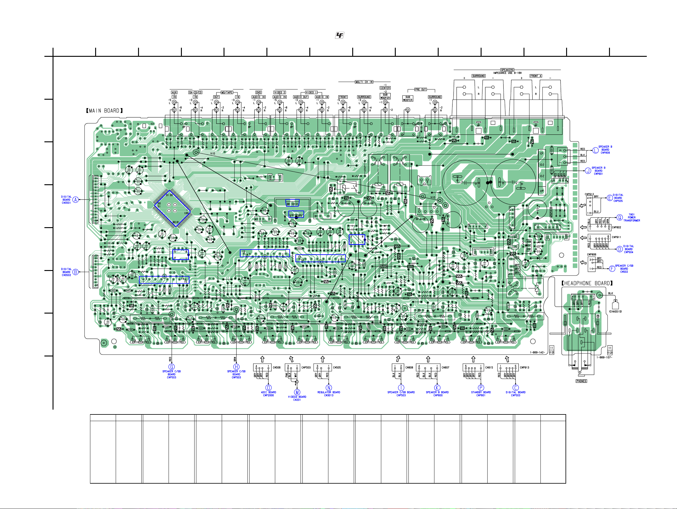
4-7. PRINTED WIRING BOARDS — MAIN SECTION — • Refer to page 12 for Circuit Boards Location. : Uses unleaded solder.
1
A
B
C
D
E
F
G
H
234567891011 12 13 14
JW791
CNP791
TP701
C790
BT790
C791
J791
IC401
JW628
Q653Q703 Q704
JW707
JW630
Q654 Q753 Q603 Q604
JW735
JW736
JW706
JW703
Q503 Q504
CC08
CC58
CC07
CC57
CC05
CC55
CC09
CC59
CC02
CC52
CC01
CC51
CNP503
CC36
CC35
CC34
CC33
CC32
CC31
CC56
CC04
CC54
JW611
JW755
JW613
JW612
JW720
JW722
JW752
JW716
JWH108
JW717
JW751
JW614
JW818
CC06
JW753
CC15
CC13
JW770
JWB01
JWB03
JW714
JW568
Q754
JW602
JW584
JW569
JW817
JW816
JW581
JW582
JW578
JW615
JW626
JW
H
112
JW507
JW708
CN807
JW767
Q534Q533
JW453
JW320
JW424
JW418
JW420
JW620
JW836
RR13
JW508
JWB02
JW800
JW813
Q692
R532
IC801
Q752
R454
C554
R747
R455
R480
C621
D722
R748
R614
RY560
R648
R695
Q572
R731
C468
L701
R766
C656
R775
R681
Q535
R407
Q571
R517
Q680
R402
R434
R405
R676
R675
L601
R404
R562
Q755
R794
R736
C517
Q506
R638
Q750
R408
R756
R755
R431
R432
R603
R458
R657
R693
R757
L651
R456
C810
R406
C767
R733
R621
R780
R457
R771
D750
R772
R761
R763
D802
R436
R667
Q691
Q722
D732
D721
C681
R764
R721
D791
C576
R502
Q560
C619
C669
C504
R703
C531
CNP501
R620
R433
Q602
R616
R622
R617
C655
R625
Q605
R778
R610
R624
C752
L751
C488
C805
D680
R792
C519
Q606
R516
R704
R671
R520
R522
R556
R555
R521
R515
Q702
R510
C577
R511
R473
R557
R680
R524
R540
C511
R714
R554
R573
R513
D505
R575
Q701
Q652
R623
R666
R475
R669
D665
R696
C670
D610
R429
Q756
Q793
D540
R692
C661
R665
R750
Q740
R526
C642
D691
R660
R773
Q640
R661
R640
R677
Q723
R737
C720
Q795
R663
Q655
Q710
R561
R719
C761
R767
R716
D740
C565
R715
Q651
Q601
R710
D765
R711
R723
R514
R760
Q502
R722
R746
R745
C464
R656
R655
R533
Q705
R673
R674
R664
R758
R602
R690
IC402
D705
C711
R586
Q751
R535
R713
Q505
Q725
C567
R694
CNP802
R806
C691
Q580
C507
IC691
Q790
R476
D560
C809
D690
C654
R474
Q501
R572
Q540
R724
R534
Q610
R611
C581
D585
R804
C716
C505
R452
Q536
R530
R587
C611
D896
C757
R588
C707
Q801
R740
R752
C566
R702
R701
R754
C756
C705
C704
C706
R651
R652
C754
C607
C605
IC701
C657
R653
R654
R604
C606
Q706
R537
R601
R451
C604
R580
C755
IC601
D580
D640
R409
R523
C620
C806
IC501
R699
C499
C469
R735
C666
Q656
R428
D804
R546
C717
C541
C742
C516
R401
D605
R734
R618
R634
R668
R802
R718
R768
R791
R793
D801
D808
D805
D806
D807
C830
C831
R613
R615
R574
R576
R570
R571
R672
JW445
TP800
CNP912
C540
R769
C770
R741
R717
R744
R753
C506
R505
R503
C580
C570
C510
C710
C740
C660
C640
C760
C680
C610
C801
C802
C822
C791
C721
C722
C750
C743
C603
C601
C653
C651
C751
C753
C703
C701
C744
C733
C732
C807
C808
C484
C493
C481
C492
C485
C490
C471
C495
C472
C553
C501
C503
C741
C459 C409
C702
C762
C458
C408
C561
CN915
CNP806
CN507
C832
Q693
Q694
D692
D693
R700
R705
JW610
R698
J
W
H
1
1
6
D710
JWH114
JW820
R631
JW559
JW757
JW754
JW702
R435
JW436
R553
R585
JW637
JW636
JW321
JW322
CN506
JW701
R525
R751
JW440
JW439
JW410
JW409
JW317
C500
C512
JW318
C811
JW311
JW312
C513
C518
C520
C523
JW450
R910
CNP911
CNP913
CN808
RR12
JW774
JW763
R706
Q695
R732
JW451
JW738
JW510
JW802
JW803
JW806
JW807
JW808
JW715
JW719
JW721
RR14
JW783
C310
CC17
JW443
C521
C522
R499
R501
JW463
JW466
JW467
JW468
JW469
JW313
JW314
JW315
JW316
JW809
JW710
C482 C483
R697
C804
C803
R803
JW712
JW601
R531
C539
JW444
JW718
JW711
JW713
R765
C766
JW431
R743
JW819
JW771
CNP801
RY791
RY701
RY601
R469
R468
R470
C445
JW464
JW465
JW416
C444
JW419
JW430
C403
C453
C463
JW461
R459
JWH118
JW810
JW811
JW812
JW723
JW414
R689
WP101
WP102
RR11
TM601
CC11
R691
J403 J404
J309
J401
J400
JWH122
JWH117
TP801
R725
C400
J310
R310
R320
R311
R321
JW506
JW432
JW458
JW455
JW454
JW425
JW438
JW411
JW415
WP100
JW470
JW435
JW428
CNP500
JW437
WP02
WP03
WP04
JW412
JW413
JW452
JW323
JW324
JW474
JW429
JW840
JW509
JW456
IC802
CN505
CN792
JW804
JW805
D505 F-5
D540 F-4
D560 D-7
D580 F-1
D585 F-2
D605 F-11
D610 D-8
D640 F-8
D665 F-8
D680 F-10
D690 E-8
• Semiconductor Location
Ref. No. Location Ref. No. Location Ref. No. Location Ref. No. Location
D691 E-8
D692 D-8
D693 D-8
D705 F-6
D710 D-9
D721 F-10
D722 E-10
D732 F-11
D740 F-5
D750 F-8
D765 F-10
D791 F-12
D801 E-12
D802 C-12
D804 E-12
D805 D-12
D806 D-12
D807 D-12
D808 D-12
D896 D-6
IC401 D-3
IC402 E-4
IC501 F-3
IC601 E-7
IC691 E-8
IC701 E-6
IC801 D-6
IC802 D-6
Q501 F-3
Q502 G-4
Q503 G-4
Ref. No. Location
Q504 G-5
Q505 G-5
Q506 F-4
Q533 G-3
Q534 G-3
Q535 G-3
Q536 F-3
Q540 F-4
Q560 D-8
Q571 F-2
Q572 G-3
Q580 G-2
Q601 G-11
Q602 G-11
Q603 G-10
Q604 G-11
Q605 F-12
Q606 F-11
Q610 D-8
Q640 F-7
Q651 F-7
Q652 G-8
Q653 G-7
Q654 G-8
Q655 F-8
Q656 G-8
Q680 F-10
Q691 E-9
Q692 E-8
Q693 D-8
Q694 D-8
Q695 E-9
Q701 F-5
Ref. No. Location Ref. No. Location
Q702 G-6
Q703 G-6
Q704 G-6
Q705 G-7
Q706 F-6
Q710 D-9
Q722 E-10
Q723 E-11
Q725 E-10
Q740 F-6
Q750 F-9
Ref. No. Location
Q751 F-9
Q752 G-9
Q753 G-9
Q754 G-10
Q755 F-10
Q756 G-10
Q790 F-12
Q793 F-11
Q795 E-10
Q801 E-12
Ref. No. Location
(Page 24)
(Page 24)
(Page 30)
(Page 30)
(Page 40)
(Page 36)
(Page 36)
(Page 30) (Page 30)
(Page 43) (Page 24)
(Page 30)
(Page 24)
(Page 43)
(Page 24)
(Page 30)
(Page 30)
STR-DG700
2020
STR-DG700
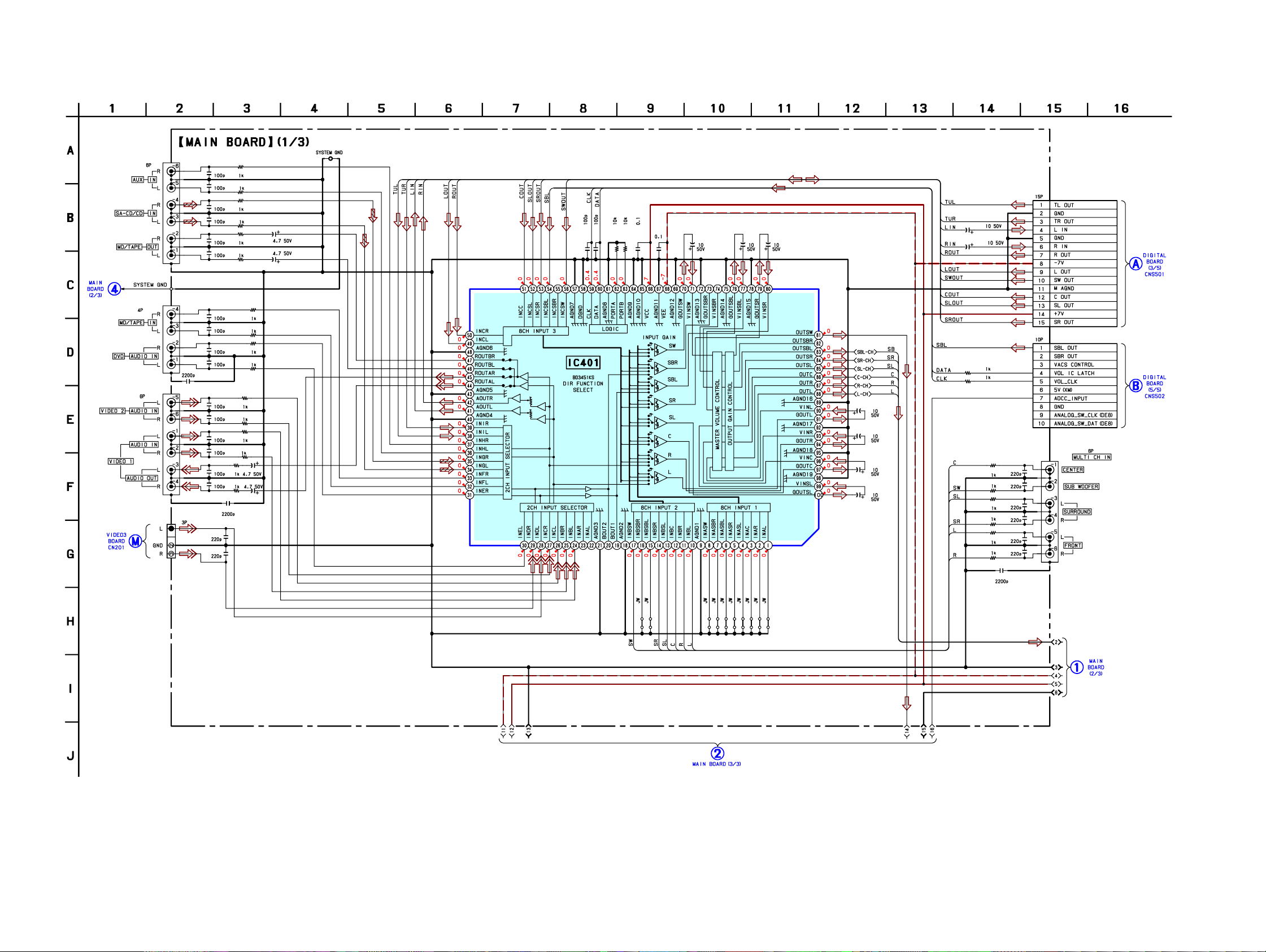
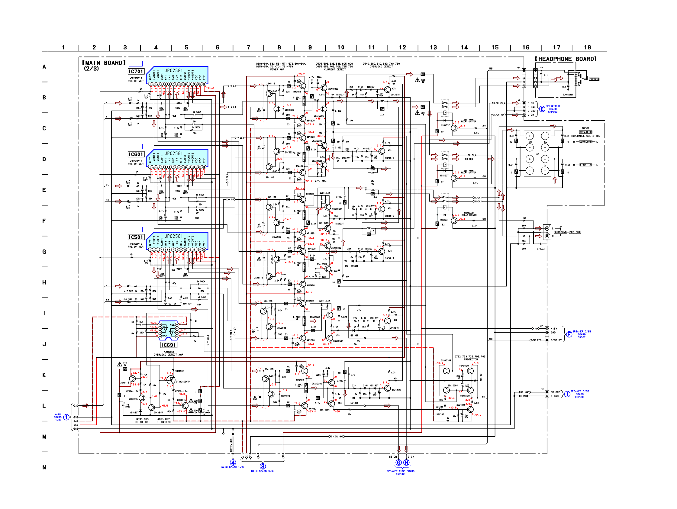
4-8. SCHEMATIC DIAGRAM — MAIN SECTION (1/3) —
R407
R457
R406
R456
R408
R458
C408
C458
R405
R455
R404
R454
R402
R452
R401
R451
R436
R435
R434
R433
R432
R431
C485C495
C488
R459
R409
C468
C469
C445
C463
C453
R475
R476
C403
CNP503
CNP501
J403
C444
C762
C702
R428
R429
CNP500
C464
IC401
J400
WP100
CC52
CC02
CC59
CC09
CC54
CC04
CC55
CC05
CC07
CC57
CC06
CC56
CC08
CC58
C490
C482
C483
C500
C512
C513
C518
C520
C521
C522
C523
J401
J404
CC36
CC35
CC34
CC33
CC32
CC31
C492
C481
C484
C493
C459
C409
CC51
CC01
(Page 21)
(Page 37)
(Page 22)
(Page 21)
(Page 27)
(Page 29)
STR-DG700
21 21
STR-DG700
4-9. SCHEMATIC DIAGRAM — MAIN SECTION (2/3) — • Refer to page 45 for IC Block Diagrams.
IC B/D
IC B/D
IC B/D
D710
R737
C722
D721
R753
R703
C755
C705
L701
R669 C670
L651
Q722
Q725
R735
C721
R736
L601
R620C619
R623
R701
R751
L751
R769 C770
R603
R653
R654
C605
C655
R651
R601
R731
C706
C756
C656
C606
R604
C707
C757
C657
C607
R501
R505
R503
R520C519
C540
D540
C640
D640
C750
C701
C751
C651
C601
D791
R791
Q706
R674 D665
Q606
R625
R624
D605
Q755
R775
R778 D765
R524 D505
R744
R743
R718
R618
Q703
Q704
R714
R715
Q701
Q653
Q654
R665
R664
Q651
Q603
Q602
Q604
R614
R615
Q601
R765
Q754
Q753
Q752
Q503
Q504
R514
R515
C680
D680
R695
R698
C732
C691
R793
R734
C642
C681
C752
C541
R780
D690
R690
D610
R634
R631
C744
C740
D740
D705R724
C742
R741
C741
C506
C505
R553
Q795
C791
R671
R621
R771
R521
Q695
R540
Q540
R557
R640
Q640
R677
R750
Q750
R757
Q691
Q692
R680
Q680
R657
R694
R648
R681
R758
R546
R699
R740
Q740R747R748
Q693
R697
R700
R705
R689
Q694
CNP806
CN808
CN807
CN792
RY601
RY701
RY791
R702
R752
C753 C703
R704
R754
C743
R652
R602
C653
C603
R733
C733
R732
R693
C507 R502C501
C610
R713
R711
R710
Q702
R663
R725
C711
R717
R723
R673
C661
R667
R638
R719
R745
R675
R755
R555
R585
R655
C720
Q705
Q652
C660
R660
R661
Q656
R672
Q655
R668
Q605
R622
R617
C611
R611
R610
R613
R763
C760
R761R760
Q751
R764
R772
Q756
C761
R773
R767
R522
Q506
R511
R510
Q501
C510
Q502
R513
C710
R722
R721
Q793
D722
Q723
R794
R792
CC11
RR11
RR13
CC15 CC17
RR14
CC13
RR12
R768
Q505
R573
C511
R517
Q571
C570
C580
Q572
R570
R571
R574
R575
R576
Q533
Q534
R531
Q535
C539
R530
R537
C531
R523
R572
R534
R535
D585
R588
R580 C581
R587
D580
Q580
R716
R666
R616
R766
R516
R526
Q536
D732
D691
D692
Q790
Q710
Q610
CNP791
J791
C790
C791
R525
WP03
WP02
IC701
IC601
IC501
C566
C504
C554
C553 C503
R561
C567
R562
C654
C604
C704
C754
C565
TP701
TM601
R311
R320
R321
R310
C310
J310
WP102
D750
R554
C561
R696
IC691
R706
R691
R692
D693
C717
C576
C577
C516
C517
C766
C767
C620
C621
C666
C669
C716
WP101
R586
R556
R756
R656
R676
R746
(Page 20)
(Page 20)
(Page 22)
(Page 31)
(Page 31)
(Page 31)
(Page 31)
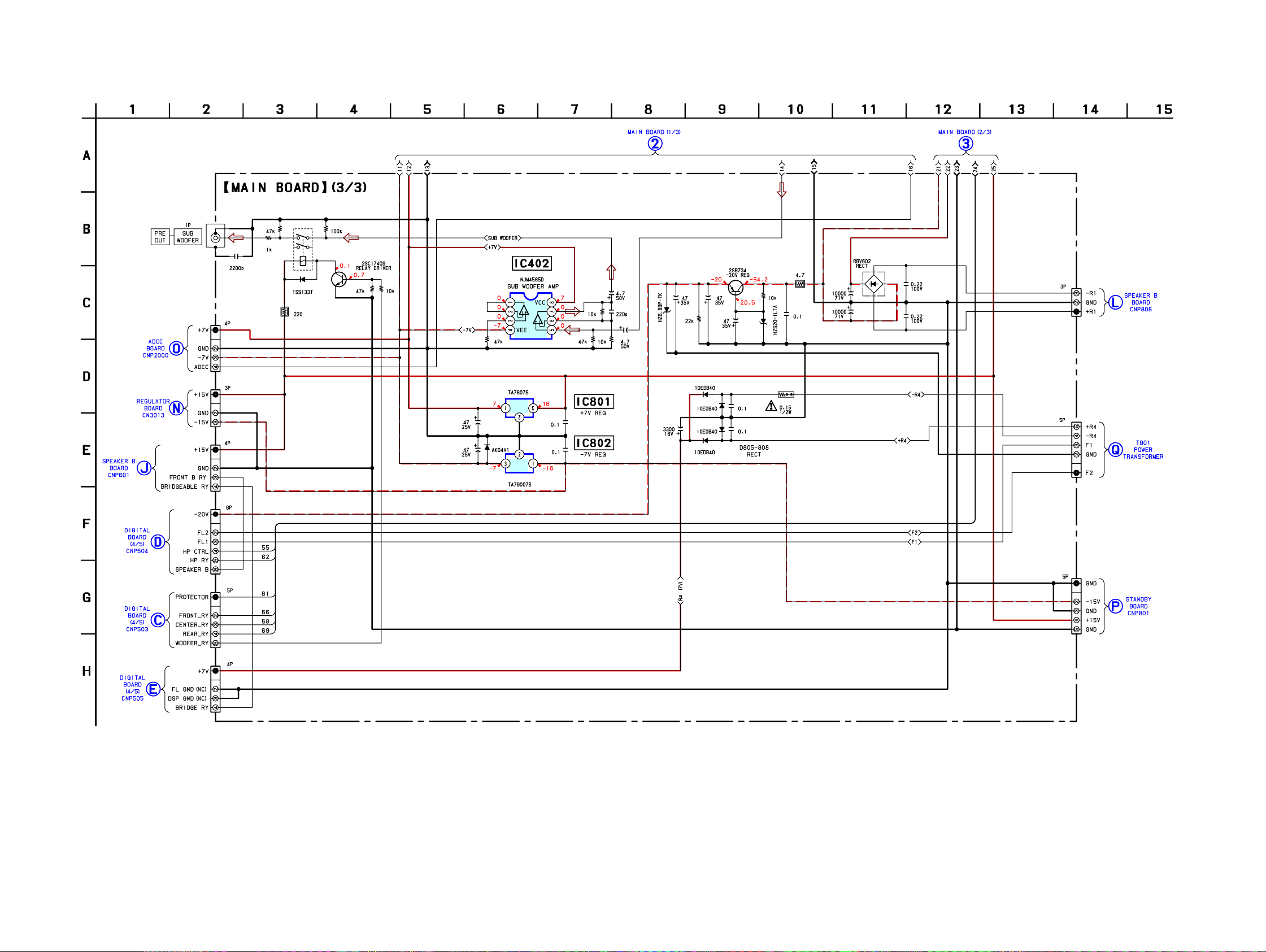
STR-DG700
2222
STR-DG700
4-10. SCHEMATIC DIAGRAM — MAIN SECTION (3/3) —
C808
D560
R474
R473
C471
R499
R532R533
C499
C810
C807
R470
C801
C802
R803
D801
D804
R802
C822
R806
C472R480
C811
C400
R468
C809
D808
C805
C806
D896
R469
CN505
CN507
CNP911
CNP913
CNP912
CNP801
CNP802
RY560
IC801
IC802
D805 C831
C830D806
D807
C832
R804
J309
D802
C803
C804
Q801
CN915
Q560
CN506
IC402
R910
(Page 28)
(Page 28)
(Page 28)
(Page 31)
(Page 37)
(Page 40)
(Page 20) (Page 21)
(Page 31)
(Page 44)
(Page 44)
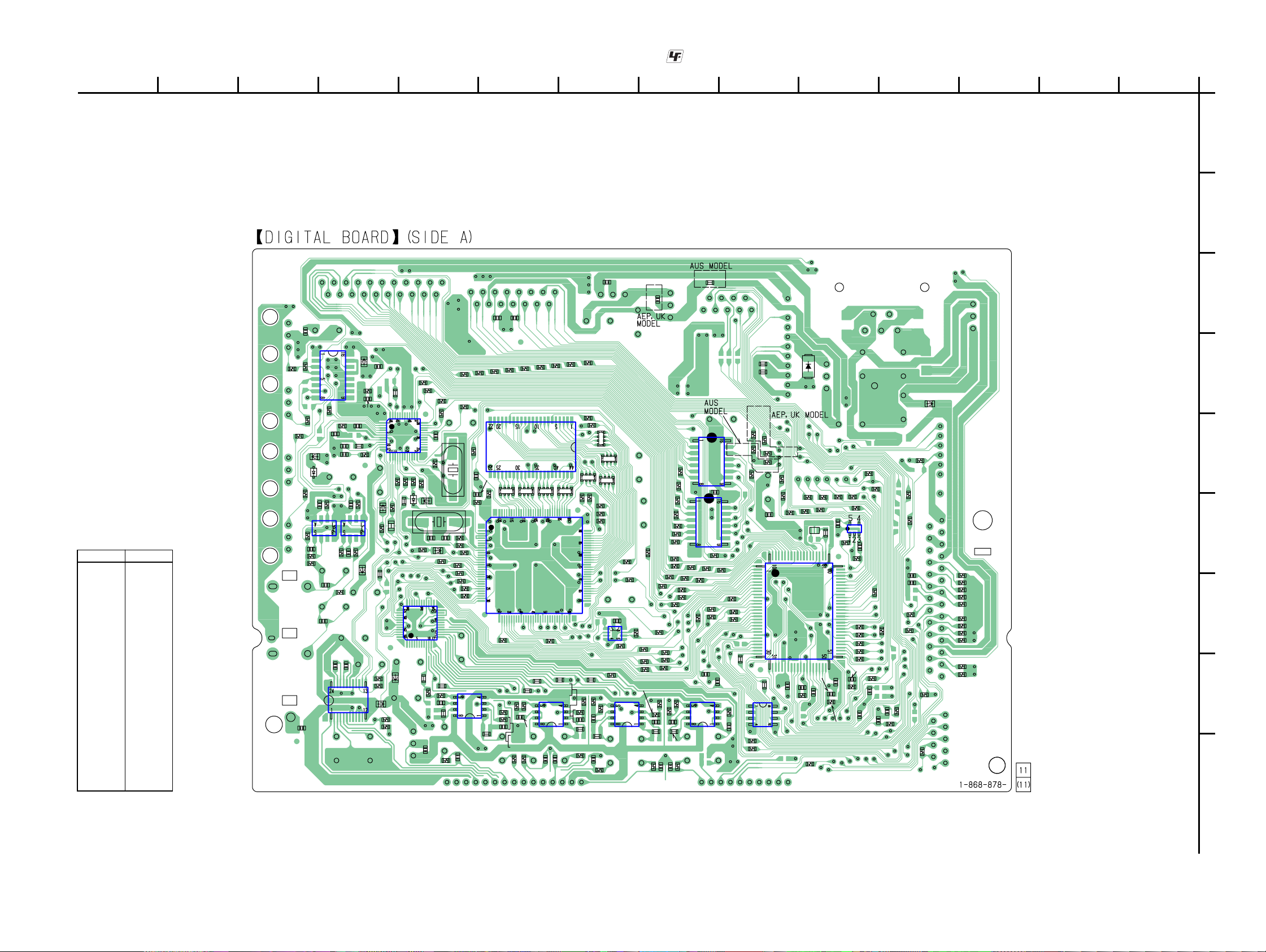
STR-DG700
23 23
STR-DG700
4-11. PRINTED WIRING BOARD — DIGITAL SECTION (1/2) — • Refer to page 12 for Circuit Boards Location. : Uses unleaded solder.
1
A
B
C
D
E
F
G
H
I
234567891011121314
IC1302
IC1103
IC1403
IC1404
IC1405
IC1406
C1045
R1060
R1057
R1421
R1085
R1086
R1175
C1141
FB1309
IC1301
R1353
R1351
R1352
R1304
C1304
R1354
C1125
R1055
C1441
C1432
R1361
C1316
C1422
C1063
R1492
R1483
C1483
R1444
R1491
R1470
R1473
C1472
R1434
R1495
R1463
R1493
C1462
R1424
R1494
R1454
R1490
C1451
R1414
C1411
JR1007
C1133
R1058
R1059
R1194
R1094
R1095
JR1202
IC1501
RB1506
IC1303
R1357
R1359
R1358
R1356
C1315
IC1401
R1436
R1486
R1426
R1416
R1476
R1466
IC1502
R1511
R1402
C1566
C1569
C1567
R1161
C1568
R1401
R1144
C1408
C1405
FB1405
C1487
FB1452
C1361
C1357
C1360
R1407
R1504
FB1306
C1301
C1302
R1301
R1446
C1303
R1360
JR1511
R1306
R1307
R1308
R1309
R1310
FB1305
X1301
JR1020
R1502
R1505
R1507
IC1602
R1152
R1153
R1154
R1155
R1151
R1044
R1523
R1506
IC1503
R1142
R1121
R1114
R1113
IC1131
RB1501
R1503
RB1502
R1078
RB1504
X1502
RB1503
RB1508
RB1507
R1125
R1126
R1185
R1557
R1514
RB1500
R1014
R1015
R1016
R1017
R1311
R1012
R1013
R1312
R1313
R1315
R1316
R1318
R1570
R1134
R1135
R1136
R1137
R1509
R1140
R1508
C1102
R1188
R1062
R1129
R1124
R1191
R1192
C1557
R1122
C1131
C1107
R1081
R1571
R1512
R1143
R1150
R1501
R1041
R1042
R1513
R1049
C1002
R1362
R1065
R1066
R1067
R1068
R1115
R1111
R1112
IC1111
R1127
R1128
R1119
C2217
R1118
R1123
R1107
R1108
R1109
R1110
R1106
C1137
R1189
R1011
X1101
R1187
R1088
R1182
R1183
R1184
R1181
C1142
R1072
R1073
R1083
C1254
C1255
C1253
C1502
R1160
R1120
C1509
C1511
R1555
R1162
R1061
C1522
R1097
C1122
C1123
C1132
C1129
C1130
C1118
C1119
C1604
C1605
R1117
R1636
R1063
R1035
R1515
FB1308
C1620
R1076
R1010
R1635
IC1601
R1572
R1573
R1149
FB1453
C1521
R1116
C1251
C1913
R1510
R1574
D1001
R1403
R1541
IC1101
R1179
R1180
R1171
R1172
R1556
R1305
R1056
C1046
IC1452
FB1503
R1077
D1302
D1301
C1362
R1322
R1319
R1460
R1461
R1484
R1445
R1471
R1472
R1475
R1420
R1435
R1464
R1425
R1455
R1157
R1156
R1524
C1105
C1104
R1103
R1202
R1203
R1303
D1001 D-5
D1301 F-10
D1302 E-12
IC1101 G-5
IC1103 F-11
IC1111 F-5
IC1131 H-6
IC1301 E-10
IC1302 D-11
IC1303 F-11
IC1401 H-11
IC1403 H-10
IC1404 H-9
IC1405 H-8
IC1406 H-7
IC1452 G-10
IC1501 F-9
IC1502 E-9
IC1503 G-8
IC1601 F-7
IC1602 E-7
• Semiconductor
Location (Side A)
Ref. No. Location

STR-DG700
2424
STR-DG700
4-12. PRINTED WIRING BOARD — DIGITAL SECTION (2/2) — • Refer to page 12 for Circuit Boards Location. : Uses unleaded solder.
1
A
B
C
D
E
F
G
H
I
234567891011 12 13 14
JR1207
C1442
C1473
C1433
C1423
C1453
C1413
R1366
C1481
C1463
C1312
R1320
C1128
R1193
JR1015
JR1016
C1314
R1355
C1494
C1547
C1454
C1401
C1409
C1404
C1450
R1314
C1310
C1520
R1251
R1530
R1186
C1172
C1100
C1140
R1039
R1190
C1108
C1171
R1105
C1358
C1021
JR1104
C1510
C2216
C1005
C1601
C1602
C1138
C1309
C1299
C1121
C1144
R1261
R1260
C1145
R1252
C1146
C1252
C1305
C1313
C1308
C1149
C1504
C1505
C1506
C1507
C1508
C1514
C1503
C1513
C1519
R1096
C1495
D1108
R1082
R1159
C1139
C1124
C1120
C1501
C1518
C1905
FB1501
FB1502
FB1101
FB1302
C1031
C1516
R1474
FB2034
C1004
C1351
C1352
C1353
C1354
D1107
D1110
D1111
D1004
D1003
D1504
D1502
D1503
D1501
JR1019
J1301
CNS508
TN1
IC1071
CNS505
CNS509
CNS502
IC1001
CNS501
CNS504
CNP503
CNP504
IC1904
IC1031
IC1902
CNP505
IC1901
IC1351
IC1352
IC1353
IC1354
C1355
C1457
C1402
C1403
C1491
C1001
C1460
C1407
C1406
C1448
C1438
C1468
C1418C1458
C1478
C1488
C1103
C2218
C1064
C1914
C1306
C1134
C1317
C1525
C1517
C1515
C1022
C1032
C1906
C1908
C1359
C1047
C1428
(Page 19)
(Page 19)
(Page 41)
(Page 19)
(Page 19)
(Page 43)
(Page 19)
(Page 33)
D1003 G-10
D1004 G-10
D1107 F-5
D1108 F-5
D1110 F-5
• Semiconductor Location (Side B)
Ref. No. Location
( ): AEP, UK model
D1111 F-5
D1501 F-10
D1502 F-10
D1503 F-10
D1504 F-10
Ref. No. Location
IC1001 I-10
IC1031 C-3
(IC1071) C-7
IC1351 D-12
IC1352 E-12
Ref. No. Location Ref. No. Location
IC1353 F-12
IC1354 C-12
IC1901 C-4
IC1902 C-8
IC1904 D-5
Loading...