


SM5K3
DESCRIPTION
The SM5K3/5K4/5K5 are CMOS 4-bit single-chip
microcomputers incorporating 4-bit parallel processing function, ROM, RAM, 10-bit A/D converter
and timer/counters.
It provides three kinds of interrupts and 4 levels
subroutine stack. Being fabricated through CMOS
process, the chip requires less power and available
in a small package : best suitable for Low power
controlling, compact equipment like a precision
charger.
FEATURES
• ROM capacity : 2 048 x 8 bits
• RAM capacity : 128 x 4 bits
• Instruction sets : 50
• Subroutine nesting : 4 levels
• I/O port :
Input 8
Output 4
Input/output 12 (36QFP/32SOP)
11 (30SDIP)
8 (28SOP)
• Interrupts :
Internal interrupt x 1 (timer)
External interrupt x 2 (2 external interrupt
inputs)
• A/D converter :
Resolution 10 bits
Channels 4
• Timer/counter : 8-bit x 1
• Built-in main clock oscillator for system clock
Ceramic/crystal oscillator (SM5K3/5K5)
CR oscillator (SM5K4)
•
Signal generation for real time clock∗(SM5K3/5K5)
• Built-in 15 stages divider
(
for real time clock∗: SM5K3/5K5)
• Instruction cycle time :
1 µs (MIN.) (2 MHz, at 5 V ± 10%) (SM5K3/5K5)
2 µs (MIN.) (1 MHz, at 2.2 to 5.5 V) (SM5K3/5K5)
1 µs (MIN.) (1.67 MHz ± 20%, at 5 V ± 10%) (SM5K4)
• Large current output pins (LED direct drive) :
15mA (TYP.)
x 4
(sink current)
•
Supply voltages :
2.2 to 5.5 V (SM5K3/5K5)
2.7 to 5.5 V (SM5K4)
•
Packages :
30-pin SDIP (SDIP030-P-0400)
32-pin SOP (SOP032-P-0525)
36-pin QFP (QFP036-P-1010)
28-pin SOP (SOP028-P-0450) (SM5K3/5K5)
24-pin SSOP (SSOP024-P-0275) (SM5K4)
∗
In case of using crystal oscillator
SM5K3/SM5K4/SM5K5
SM5K3/SM5K4
SM5K5
4-Bit Single-Chip Microcomputers
(Controllers With 10-Bit A/D Converter)
- 1 -
In the absence of confirmation by device specification sheets, SHARP takes no responsibility for any defects that may occur in equipment using any SHARP devices shown in catalogs, data books,
etc. Contact SHARP in order to obtain the latest device specification sheets before using any SHARP device.
- 2 -
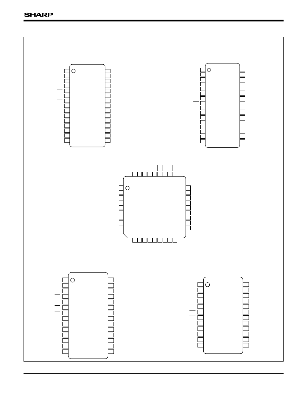
36-PIN QFP
10
11
12
13
14
P4
1
P42
P43
P00
P01
P02
P03
P10
P11
P12
P13
P20
P21
P22
28
27
26
25
24
23
22
21
20
19
18
17
16
15
GND
P4
0
AGND
P3
3
P32
P31
P30
VR
RESET
V
DD
OSCOUT
OSCIN
P23
GND
1
2
3
4
5
6
7
8
9
SM5K3/SM5K4/SM5K5
PIN CONNECTIONS
P53
P41
P42
P43
P00
P01
P02
P03
P10
P11
P12
P13
P20
P21
P22
30
29
28
27
26
25
24
23
22
21
20
19
18
17
16
GND
P4
0
AGND
P3
3
P32
P31
P30
VR
RESET
V
DD
OSCOUT
OSCIN
P23
P51
P50
1
2
3
4
5
6
7
8
9
10
11
12
13
14
15
10
11
12
13
14
15
16
P5
3
P41
P42
P43
P00
P01
P02
P03
P10
P11
P12
P13
P20
P21
P22
GND
32
31
30
29
28
27
26
25
24
23
22
21
20
19
18
17
GND
P5
2
P40
AGND
P3
3
P32
P31
P30
VR
RESET
V
DD
OSCOUT
OSCIN
P23
P51
P50
1
2
3
4
5
6
7
8
9
30-PIN SDIP 32-PIN SOP
TOP VIEW
28-PIN SOP (SM5K3/5K5)
10
11
12
P4
1
P42
P43
P00
P01
P02
P03
P10
P11
P20
P21
P22
24
23
22
21
20
19
18
17
16
15
14
13
GND
P4
0
AGND
P3
2
P31
P30
VR
RESET
V
DD
OSCOUT
OSCIN
P23
1
2
3
4
5
6
7
8
9
24-PIN SSOP (SM5K4)
P13
P12
P11
P10
(NC)
P03
P02
P01
29 28
P20
P21
P22
(NC)
GND
P50
P51
P23
OSCIN
36 35 34 33 32 31 30
1
2
3
4
5
6
7
8
9
P00
P43
27
P42
26
P41
25
P53
24
GND
23
(NC)
22
P52
21
P40
20
AGND
19
10 1112 13 14 15 16 17 18
VR
P31
P32
P33
RESET
(NC)
P30
VDD
OSCOUT
- 3 -
SM5K3/SM5K4/SM5K5
BLOCK DIAGRAM
Nomenclature
A : A register
A/D : A/D converter unit
ALU : Arithmetic logic unit
B
M, BL : RAM address register
C : Carry flag
IFA, IFB, IFT : Interrupt request flag
IME : Interrupt master enable flag
INST. DEC. : Instruction decoder
INT : Interrupt control unit
P0-P5 : Port register
P
U, PL : Program counter
R8, R9, RC, RE, RF
: Mode register
RA : Count register
RB : Modulo register
SB : SB register
SR : Stack register
P00
P01
P02
P03
P10
P11
P12
P13
P20
P21
P22
P23
P30
P31
P32
P33
P40
P41
P42
P43
P50
P51
P52
P53
P2
P0
P1
P3 P4 P5
IFT IFAIFB
FR R3
INT
A/D
VR
AGND
OSC
RC RB
RE
SR x 4
PRESCALER
SR (8)
P
U (5) PL (6)
B
M (4) BL (4)
IME
RA
INTERRUPT
CONTROLLER
DECDEC
X (4)
A (4)
C
ALU
ROM
VDD
GND
OSC
IN
OSCOUT
RESET
2 048-BYTE
128 x 4-BIT
RAM
R8
R9
INST.DEC.
SELECTOR
ALU
- 4 -
PARAMETER
SM5K3/SM5K4/SM5K5
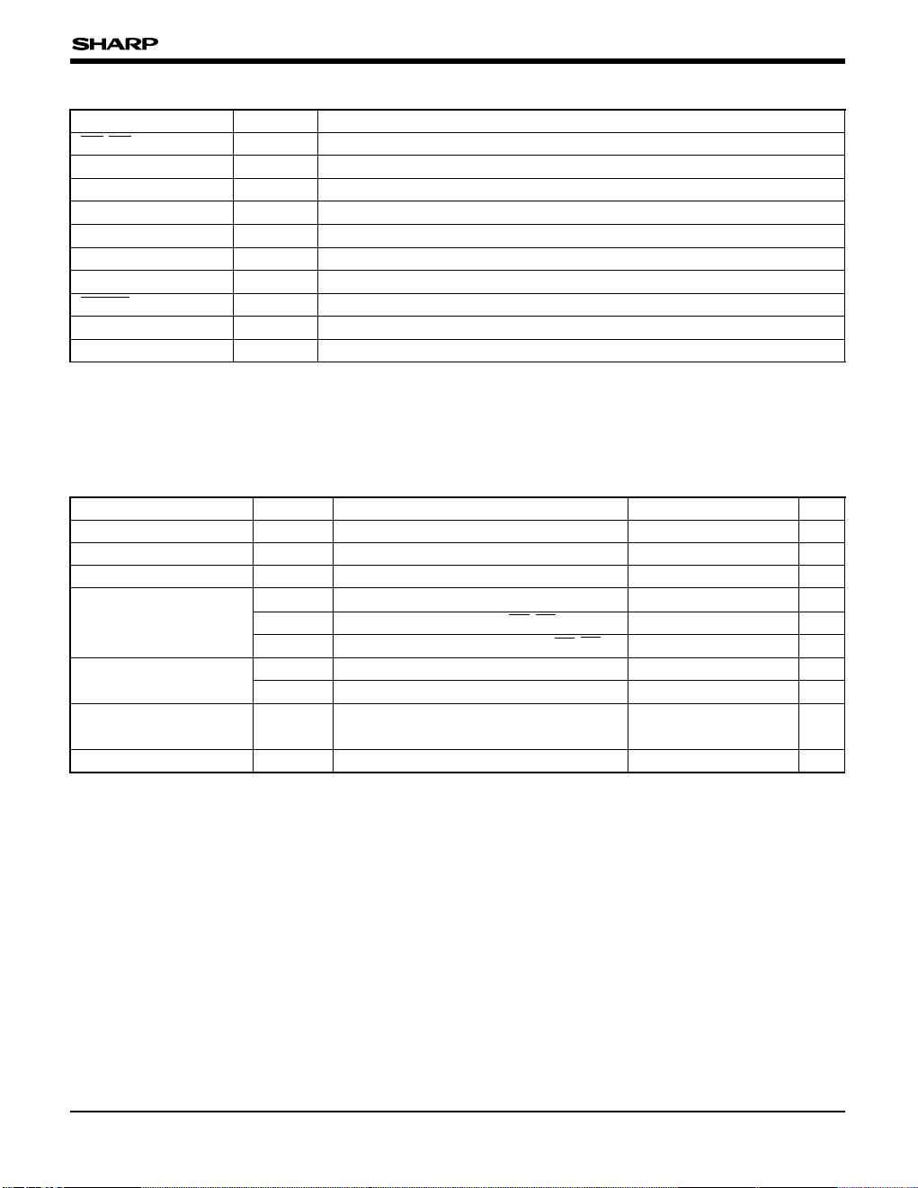
PIN DESCRIPTION
ABSOLUTE MAXIMUM RATINGS
SYMBOL I/O FUNCTION
P00-P03
O High current output (sink current 15 mA)
P10-P11 I Input (standby release) (counter input : P11) with pull-up resistor
P12-P13 I Input (standby release) with pull-up resistor
P20-P23 I/O Input (with pull-up resistor) or output (independent)
P30-P33 I Input (also used as analog input) with pull-up resistor
P40-P43, P50-P53 I/O Input (with pull-up resistor) and output
OSCIN, OSCOUT I/O Ceramic/crystal oscillation pin (SM5K3/5K5)/CR oscillation pin (SM5K4)
RESET
I Reset signal input with pull-up resistor
VR, AGND I A/D converter reference supply input port
VDD, GND I Power supply, Ground
SYMBOL CONDITIONS RATING UNIT
Supply voltage VDD – 0.3 to +7.0 V
Input voltage VI – 0.3 to VDD+0.3 V
Output voltage VO – 0.3 to VDD+0.3 V
Maximum output current
IOH High-level output current (all outputs) 4 mA
IOL0 Low-level output current (
P0
0-P03
) 30 mA
IOL1
Low-level output current (all but P00-P03)
4 mA
Total output current
∑IOH High-level output current (all outputs) 20 mA
∑IOL Low-level output current (all outputs) 80 mA
TOPR
–20 to +70 (SM5K3/5K5)
–20 to +85 (SM5K4)
°C
Storage temperature
TSTG –55 to +150 °C
Operating temperature
NOTE :
Symbols apply to 32-pin SOP and 36-pin QFP. (
In case of 30-pin SDIP, P52does not exist. In case of 28-pin SOP, P50-P53do not exist.
In case of 24-pin SSOP, P12, P13, P33, P50-P53 pins do not exist.)
- 5 -
SM5K3/SM5K4/SM5K5
RECOMMENDED OPERATING CONDITIONS
(SM5K3/5K5)
PARAMETER SYMBOL CONDITIONS RATING UNIT
Supply voltage VDD 2.2 to 5.5 V
Instruction cycle TSYS
VDD = 2.2 to 5.5 V 2 to 61
µs
VDD = 5.0 V ± 10% 1 to 61
Main clock frequency
(OSC
IN-OSCOUT)
fOSC
VDD = 2.2 to 5.5 V 1 M to 32.768 k
Hz
VDD = 5.0 V ± 10% 2 M to 32.768 k
(SM5K4)
NOTES :
• The typical oscillation frequency shall be determined in
consideration of operating condition and fluctuation
frequency.
• Mount Rf, RD, C
1, C2, Oscillator (SM5K3/5K5)/Rf (SM5K4)
as close as possible to the oscillator pins of the LSI, in
order to reduce an influence from floating capacitance.
• Since the value of resistor Rf, RD, C
1, C2, Oscillator
(SM5K3/5K5)/Rf (SM5K4) varies depending on circuit
pattern and others, the final Rf, RD, C
1, C2, Oscillator
(SM5K3/5K5)/Rf (SM5K4) value shall be determined on the
actual unit.
• Don't connect any line to OSC
IN and OSCOUT except
oscillator circuit.
• Don't put any signal line across the oscillator circuit line.
• On the multilayer circuit, do not let the oscillator circuit
wiring cross other circuit.
• Minimize the wiring capacitance of GND and V
DD .
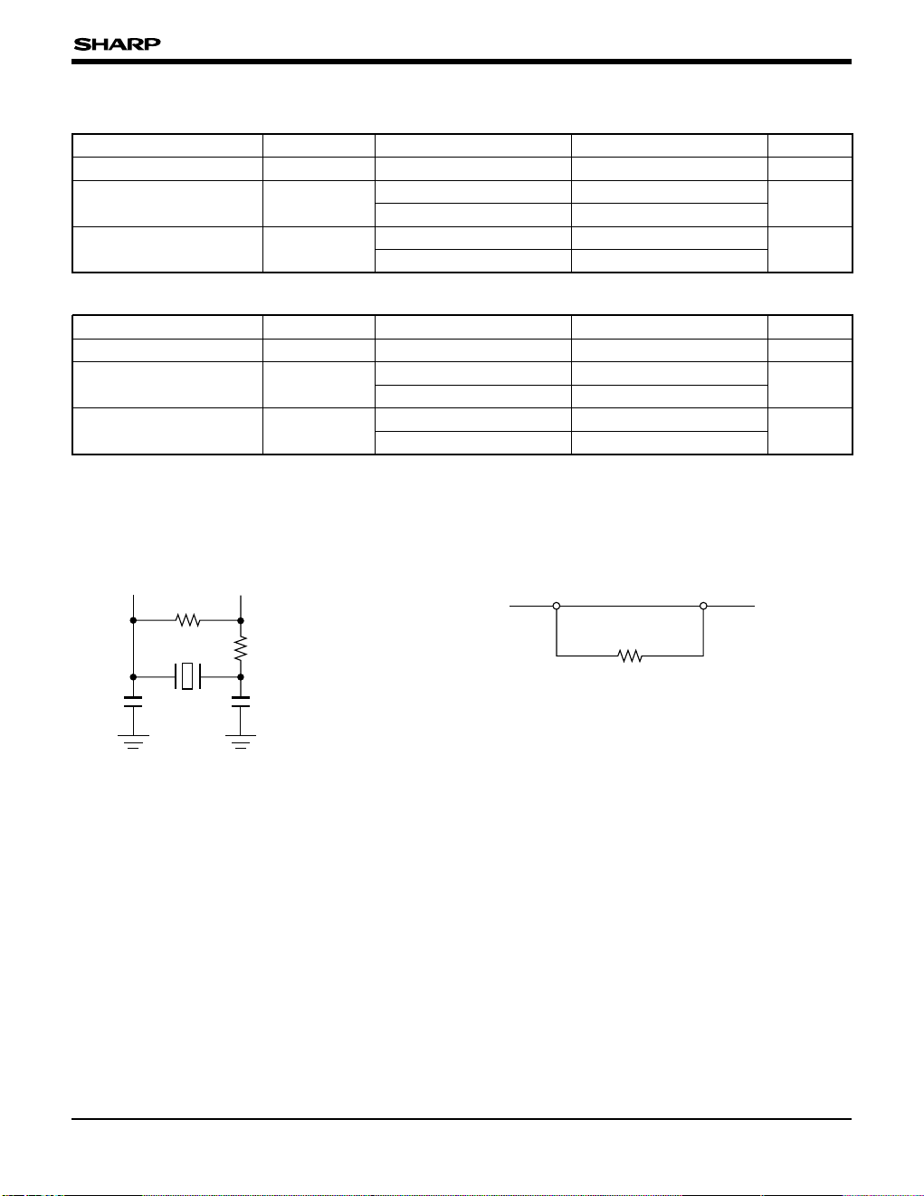
OSCILLATION CIRCUIT
PARAMETER SYMBOL CONDITIONS RATING UNIT
Supply voltage VDD 2.7 to 5.5 V
Instruction cycle TSYS
VDD = 2.7 to 5.5 V 2 to 5
µs
VDD = 5.0 V ± 10% 1 to 5
Main clock frequency ∗
(OSCIN-OSCOUT)
fOSC
VDD = 2.7 to 5.5 V 1 M to 400 k
Hz
VDD = 5.0 V ± 10% 2 M to 400 k
∗
Degree of fluctuation frequency :
± 20%
OSCOUTOSCIN
Rf
Rf = 33 kΩ
(fosc = 1.67 MHz, TYP.)
• SM5K3/5K5
∗
Reference only : Circuit configuration varies according to
oscillator used.
• SM5K4
OSCOUTOSCIN
Rf
RD
Oscillator
C
1 C2
- 6 -
NOTES :
1. Applicable pins : P12, P13, P20-P23, P30-P33 (digital input
mode), P4
0-P43 P50-P53
2. Applicable pins : OSCIN, RESET, P10, P11
3. Applicable pins : RESET, P10-P13, P20-P23, P40-P43,
P5
0-P53 (digital input mode)
4. Applicable pins : P3
0-P33 (analog input mode)
5. Applicable pins : P0
0-P03 (high current mode)
6. Applicable
pins :
P20-P23, P40-P43, P50-P53(output mode)
∗
1
7. Applicable pins : P30-P33
∗
2
8. No load (A/D conversion is stop.)
9. A/D conversion in operation (operation enable)
10. A/D conversion in stop (operation disable)
∗
1
In case of 32-pin SOP and 36-pin QFP.
(In case of 30-pin SDIP, P5
2
dose not exist. In case of
28-pin SOP, P5
0
-P53do not exist.)
∗
2
P3 ports are normally used for input ports with pull-up
resistor. These ports can be also used.
SM5K3/SM5K4/SM5K5
VIH1 0.8 x VDD VDD
V1
V
IL1 0 0.2 x VDD
VIH2 0.9 x VDD VDD
V2
V
IL2 0 0.1 x VDD
VDD = 2.2 to 3.3 V 2 25 90
I
IL1 VIN = 0 V
V
DD = 4.5 to 5.5 V 25 70 250 µA 3
I
IH1 VIN = VDD 2
I
IL2 VIN = 0 V 1.0 10
µA 4
I
IH2 VIN = VDD 1.0 10
V
DD = 2.2 to 3.3 V 5 15
I
OL1 VO = 1.0 V
V
DD = 4.5 to 5.5 V 15 25
mA 5
V
DD = 2.2 to 3.3 V 0.3 1.5
I
OH1 VO = VDD – 0.5 V
V
DD = 4.5 to 5.5 V 1.0 2.2
V
DD = 2.2 to 3.3 V 1.2 5.0
I
OL2 VO = 1.5 V
V
DD = 4.5 to 5.5 V 5 9.0
mA 6
V
DD = 2.2 to 3.3 V 0.3 2.0
I
OH2 VO = VDD – 0.5 V
V
DD = 4.5 to 5.5 V 1.0 2.4
V
DD = 2.2 to 3.3 V 0.15
I
OH3 VOH = VDD – 1.0 V mA 7
V
DD = 4.5 to 5.5 V 0.5
f
OSC = 2 MHZ
V
DD = 4.5 to 5.5 V 1 200 2 500
V
DD = 2.2 to 3.3 V 300 800
f
OSC = 1 MHz
I
DD VDD = 4.5 to 5.5 V 600 1 200
f
OSC = 32.768 kHz
V
DD = 2.2 to 3.3 V 20 120
(Crystal OSC mode)
fOSC = 2 MHz
V
DD = 4.5 to 5.5 V 760 1 500
V
DD = 2.2 to 3.3 V 200 600 µA 8
f
OSC = 1 MHz
I
HLT VDD = 4.5 to 5.5 V 400 900
f
OSC = 32.768 kHz
V
DD = 2.2 to 3.3 V 20 75
(Crystal OSC mode)
Ceramic OSC mode
VDD = 2.2 to 3.3 V 2
I
STOP fOSC = 32.768 MHz
V
DD = 2.2 to 3.3 V 15 40
(Crystal OSC mode)
A/D in operation
V
DD = 4.5 to 5.5 V 220 450 µA 9
I
VR
A/D in stop
V
DD = 4.5 to 5.5 V 2 µA 10
Resolution
10 bit
Differential
fOSC = 1 MHz
V
DD = VR = 5.0 V ± 2.5 ± 4.0
linearity error
TOPR = 25°C
Sequential
fOSC = 1 MHz
V
DD = VR = 5.0 V ± 3.2 ± 5.0 LSB
linearity error
TOPR = 25°C
f
OSC = 1 MHz
Total error VDD = VR = 5.0 V ± 4.0 ± 6.0
TOPR = 25°C
A/D
conversion
Input voltage
Input current
Output current
Supply cerrent
DC CHARACTERISTICS
• SM5K3 (TOPR = –20 to +70°C, TYP. value : VDD = 5.0 or 3.0 V, Unless otherwise noted.)
PARAMETER
SYMBOL
CONDITIONS MIN. TYP. MAX.
UNIT
NOTE
- 7 -
Resolution 10
Differential
fOSC = 1.0 MHz
VDD = VR = 5.0 V ± 2.5 ± 4.0
linearity error
TOPR = 25°C
Sequential
fOSC = 1 MHz
V
DD = VR = 5.0 V ± 3.2 ± 5.0
linearity error
TOPR = 25°C
f
OSC = 1 MHz
Total error V
DD = VR = 5.0 V ± 4.0 ± 6.0
T
OPR = 25°C
V
IH1 0.8 x VDD VDD
VIL1 0 0.2 x VDD
VIH2 0.9 x VDD VDD
VIL2 0 0.1 x VDD
VDD= 2.7 to 3.3 V
1.0 25 90
I
IL1 VIN = 0 V
VDD= 4.5 to 5.5 V
15 70 250
I
IH1 VIN = VDD 3.0
I
IL2 VIN = 0 V 1.0 10
I
IH2 VIN = VDD 1.0 10
VDD= 2.7 to 3.3 V
315
I
OL1 VO = 1.0 V
VDD= 4.5 to 5.5 V
12 25
VDD= 2.7 to 3.3 V
0.2 1.5
I
OH1 VO = VDD – 0.5 V
VDD= 4.5 to 5.5 V
0.8 2.2
I
OL2 VO = 1.5 V
VDD= 4.5 to 5.5 V
4.0 9.0
VDD= 2.7 to 3.3 V
0.2 2.0
I
OH2 VO = VDD – 0.5 V
VDD= 4.5 to 5.5 V
0.8 2.4
I
OH3 VOH = VDD – 1.0 V
VDD= 4.5 to 5.5 V
0.5
f
OSC = 2.0 MHz
VDD= 4.5 to 5.5 V
1 200 2 800
I
DD
VDD= 2.7 to 3.3 V
300 900
f
OSC = 1.0 MHz
VDD= 4.5 to 5.5 V
600 1 400
f
OSC = 2.0 MHz
VDD= 4.5 to 5.5 V
760 1 700
I
HLT
fOSC = 1.0 MHz
VDD= 4.5 to 5.5 V
400 1 000
I
STOPVDD
= 2.7 to 5.5 V
5
A/D conversion
VDD= 2.7 to 3.3 V
130 350
I
VR in operation
VDD= 4.5 to 5.5 V
220 500
A/D conversion in stop
VDD= 2.7 to 5.5 V
3
• SM5K4 (TOPR = –20 to +85°C, TYP. value : VDD = 5.0 or 3.0 V, Unless otherwise noted.)
SM5K3/SM5K4/SM5K5
PARAMETER SYMBOL
CONDITIONS MIN. TYP. MAX.
UNIT
NOTE
Input voltage
V 1
V 2
Input current
µA 3
µA
4
Output current
mA 5
mA
6
mA
7
Supply current
µA 8
µA
9
µA 10
A/D
conversion
Reference
clock oscillator
frequency
bit
LSB
MHz
NOTES :
1. Applicable pins : P12, P13, P20-P23, P30-P33 (digital input
mode), P4
0-P43, P50-P53
∗
1
2. Applicable pins : OSCIN, RESET, P10, P11
3. Applicable pins : RESET, P10-P13, P20-P23, P40-P43,
P5
0-P53 (digital input mode)
∗
1
4. Applicable pins : P30-P33 (analog input mode)
5. Applicable pins : P0
0-P03 (high current output)
6. Applicable
pins :
P20-P23, P40-P43, P50-P53(output mode)
∗
1
7. Applicable pins : P30-P33
∗
2
8. No load (A/D conversion in stop)
9. A/D conversion in operation (A/D conversion enable)
10. A/D conversion in stop (A/D conversion disable)
∗
1
In case of 32-pin SOP and 36-pin QFP.
(In case of 30-pin SDIP, P5
2
pin dose not exist. In case of
24-pin SSOP, P1
2
, P13, P33, P50-P53pins do not exist.)
∗
2 P3 ports are normally used for input port with pull-up
resistor. These ports can be also used as a suspected
case of output port.
fOSC
VDD= 4.5 to 5.5 V, Rf = 33 kΩ
1.34 1.67 2.0
SM5K3/SM5K4/SM5K5
- 8 -
• SM5K5 (TOPR = –20 to +70°C, TYP. value : VDD = 5.0 or 3.0 V, Unless otherwise noted.)
PARAMETER
SYMBOL
CONDITIONS MIN.
UNIT
NOTE
Input voltage
VIH1
0.8 x VDD
0
0.9 x VDD
0
VDD
0.2 x VDD
VDD
0.1 x VDD
VV1
2
Input current
IIL1
VIN = 0 V
2
25
25
70
1
1
90
250
2
10
10
µAµA3
4
Output current
IOL1 VO = 1.0 V
5
15
0.3
1.0
7
20
300
1 000
15
25
1.5
2.2
35
60
2 000
2 400
mA
µA
5
6
Supply current
IDD
fOSC = 2 MHz 1 200
300
600
20
40
760
400
15
20
2
10
130
220
2 500
800
1 200
120
160
1 500
900
60
90
2
10
25
300
450
2
µA
µA
µA
µA
7
7
8
9
A/D
conversion
Resolution 10
± 2.5
± 3.2
± 4.0
± 4.0
± 5.0
± 6.0
bit
LSB
VIH2
VIL1
VIL2
IIL2
IIH1
IIH2
IOL2
IOH1
IOH2
ISTOP
IHLT
IVR
Sequential
linearity error
Differential
linearity error
Total error
VDD = VR = 5.0 V
V
DD = VR = 5.0 V
V
DD = VR = 5.0 V
fOSC = 1 MHz
TOPR = 25°C
fOSC = 1 MHz
T
OPR = 25°C
fOSC = 1 MHz
T
OPR = 25°C
VIN = VDD
VIN = 0 V
VIN = VDD
VDD= 2.2 to 3.3 V
VDD= 4.5 to 5.5 V
VO = VDD–0.5 V
VO = 0.5 V
VO = VDD–0.5 V
VDD= 2.2 to 3.3 V
VDD= 4.5 to 5.5 V
VDD= 2.2 to 3.3 V
VDD= 4.5 to 5.5 V
VDD= 2.2 to 3.3 V
VDD= 4.5 to 5.5 V
VDD= 2.2 to 3.3 V
VDD= 4.5 to 5.5 V
VDD= 4.5 to 5.5 V
A/D in operation
Ceramic OSC mode
fOSC = 32.768 kHz
(Crystal OSC mode)
fOSC = 1 MHz
fOSC = 32.768 kHz
(Crystal OSC mode)
fOSC = 1 MHz
fOSC = 2 MHz
fOSC = 32.768 kHz
(Crystal OSC mode)
A/D in stop
VDD= 4.5 to 5.5 V
VDD= 4.5 to 5.5 V
VDD= 2.2 to 3.3 V
VDD= 2.2 to 3.3 V
VDD= 4.5 to 5.5 V
VDD= 4.5 to 5.5 V
VDD= 4.5 to 5.5 V
VDD= 2.2 to 3.3 V
VDD= 4.5 to 5.5 V
VDD= 2.2 to 5.5 V
VDD= 2.2 to 3.3 V
VDD= 4.5 to 5.5 V
VDD= 2.2 to 3.3 V
VDD= 2.2 to 3.3 V
MAX.TYP.
SM5K3/SM5K4/SM5K5
- 9 -
NOTES :
1. Applicable pins : P12, P13, P20-P23, P30-P33 (digital input
mode), P4
0-P43, P50-P53
∗
1
2. Applicable pins : OSCIN, RESET, P10, P11
3. Applicable pins : RESET, P10-P13, P20-P23, P40-P43,
P5
0-P53 (digital input mode)
∗
1
4. Applicable pins : P30-P33 (analog input mode)
5. Applicable pins : P0
0-P03 (high current port)
6. Applicable pins : P2
0-P23, P40-P43, P50-P53 (output mode)
∗
1
7. No load (A/D conversion in stop)
8. A/D conversion in operation (operation enable)
9. A/D conversion in stop (operation disable)
∗
1 In case of 32-pin SOP and 36-pin QFP.
( In case of 30-pin SDIP, P5
2 dose not exist. In case of
28-pin SOP, P5
0-P53 do not exist.)
SYSTEM CONFIGURATION
A Register and X Register
The A register (or accumulator : ACC) is a 4-bit
general purpose register. The register is mainly
used in conjunction with the ALU, C flag and RAM
to transfer numerical value and data to perform
various operations. The A register is also used to
transfer data between input and output pins.
The X register (or auxiliary accumulator) is a 4-bit
register and can be used as a temporary register.
It loads contents of the A register or its content is
transferred to the A register. When the table
reference instruction PAT is used, the X and A
registers load ROM data. A pair of A and X
registers can accommodate 8-bit data.
Arithmetic and Logic Unit (ALU) and
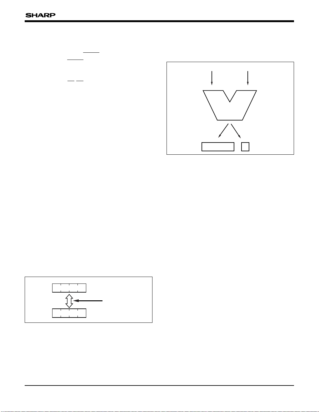
Carry Signal Cy
The ALU performs 4-bit parallel operation
The ALU operates binary addition in conjunction
with RAM, C flag and A register. The carry signal
Cy is generated if a carry occurs during ALU
operation. Some instructions use Cy : ADC
instruction sets/clears the content of the C flag;
ADX instruction causes the program to skip the
next instruction. Note that Cy is the symbol for
carry signal and not for C flag.
3
3
0
0
A register
X register
EXAX instruction
Fig. 1 Data Transfer Example between
A Register and X Register
c
Areg
ALU
Result of operation
4-bit data 4-bit data
Fig. 2 ALU
 Loading...