


LC-32PX5M/X/LC-37PX5M/X
SERVICE MANUAL
No. S17B1LC37PX5M
LCD COLOR TELEVISION
LC-32PX5M/X
MODELS LC-37PX5M/X
In the interests of user-safety (Required by safety regulations in some countries) the set should be restored to its original condition and only parts identical to those specified be used.
OUTLINE
This model is based on the LC-32BX5H/M, LC-37BX5H/M and partially modified.
For the contents not covered in this Service Manual, accordingly, please refer to the LC-32BX5H/M, LC-37BX5H/M (S56T7LC32BX5M) Service Manual.
CONTENTS
|
|
|
|||
DIFFERENCES FROM BASE MODEL |
|
CHAPTER 5. BLOCK DIAGRAM/OVERALL WIRING |
|||
|
LIST OF CHANGED PARTS ............................. |
i |
DIAGRAM |
|
|
|
|
|
[1] |
BLOCK DIAGRAM......................................... |
5-1 |
SAFETY PRECAUTION |
|
[2] OVERALL WIRING DIAGRAM (LC- |
|
||
|
IMPORTANT SERVICE SAFETY PRE- |
|
|
32PX5M/X) .................................................... |
5-3 |
|
CAUTION ......................................................... |
v |
[3] |
OVERALL WIRING DIAGRAM (LC- |
|
|
Precautions for using lead-free solder............. |
vi |
|
37PX5M/X) .................................................... |
5-5 |
CHAPTER 1. SPECIFICATIONS |
|
CHAPTER 6. SCHEMATIC DIAGRAM |
|
||
[1] |
SPECIFICATIONS......................................... |
1-1 |
[1] |
DESCRIPTION OF SCHEMATIC DIA- |
|
|
|
|
|
GRAM ............................................................ |
6-1 |
CHAPTER 2. OPERATION MANUAL |
|
[2] |
SCHEMATIC DIAGRAM ................................ |
6-2 |
|
[1] |
OPERATION MANUAL.................................. |
2-1 |
CHAPTER 7. PRINTED WIRING BOARD |
|
|
|
|
|
|
||
CHAPTER 3. DIMENSIONS |
|
[1] OPERATION UNIT PRINTED WIRING |
|
||
[1] |
DIMENSIONS................................................ |
3-1 |
|
BOARD .......................................................... |
7-1 |
|
|
|
[2] LED, R/C UNIT PRINTED WIRING |
|
|
CHAPTER 4. REMOVING OF MAJOR PARTS |
|
|
BOARD .......................................................... |
7-2 |
|
[1] REMOVING OF MAJOR PARTS................... |
4-1 |
Parts Guide |
|
||
|
|
|
|
||
|
|
|
|
|
|
Parts marked with "  " are important for maintaining the safety of the set. Be sure to replace these parts with specified ones for maintaining the safety and performance of the set.
This document has been published to be used for after sales service only.
The contents are subject to change without notice.
LC-32PX5M/X/LC-37PX5M/X
DIFFERENCES FROM BASE MODEL
LIST OF CHANGED PARTS
LC-32PX5M / LC-32PX5X
Ref. No. |
Description |
LC-32BX5M |
LC-32PX5M |
LC-32PX5X |
Note |
PRINTED WIRING BOARD ASSEMBLIES (NOT REPLACE ITEM) |
|
|
|
||
|
OPERATION Unit |
DUNTKD685FM03 |
DUNTKE097FM02 |
DUNTKE097FM02 |
Changes |
|
MAIN Unit |
DUNTKD892FM03 |
DUNTKD892FM50 |
DUNTKD892FM51 |
Changes |
|
SUB Unit |
DUNTKD893FM03 |
DUNTKD893FM50 |
DUNTKD893FM51 |
Changes |
|
LED, R/C Unit |
DUNTKD897FM03 |
DUNTKE095FM02 |
DUNTKE095FM02 |
Changes |
|
VIDEO-IN3 Unit |
DUNTKD898FM03 |
- |
- |
Delete |
|
POWER Unit exchange |
RDENCA182WJQZ |
RDENCA182WJQZ |
RDENCA182WJQZ |
No Changes |
LED, R/C UNIT (DUNTKD095FM02) |
|
|
|
|
|
J101 |
Jack |
QJAKJA014WJZZ |
- |
- |
Delete |
R111 |
Resistor 22 1/4W Metal Oxide |
VRS-TW2ED220JY |
- |
- |
Delete |
R112 |
Resistor 100k 1/16W Metal Oxide |
VRS-CY1JF104JY |
- |
- |
Delete |
R113 |
Resistor 22 1/4W Metal Oxide |
VRS-TW2ED220JY |
- |
- |
Delete |
R114 |
Resistor 100k 1/16W Metal Oxide |
VRS-CY1JF104JY |
- |
- |
Delete |
R115 |
Resistor 1k 1/16W Metal Oxide |
VRS-CY1JF102JY |
- |
- |
Delete |
SUB UNIT (DUNTKD893FM50 / DUNTKD893FM51) |
|
|
|
|
|
C1319 |
Capacitor 220 6.3V Electrolytic |
VCEASX0JN227MY |
- |
- |
Delete |
C1320 |
Capacitor 10 16V Ceramic |
RC-KZA510WJPZY |
- |
- |
Delete |
C1321 |
Capacitor 0.1 25V Ceramic |
VCKYCY1EF104ZY |
- |
- |
Delete |
C1322 |
Capacitor 220 6.3V Electrolytic |
VCEASX0JN227MY |
- |
- |
Delete |
C1326 |
Capacitor 1000p 50V Ceramic |
VCKYCY1HB102KY |
- |
- |
Delete |
C1327 |
Capacitor 1000p 50V Ceramic |
VCKYCY1HB102KY |
- |
- |
Delete |
C1328 |
Capacitor 1 10V Ceramic |
VCKYCY1AB105KY |
- |
- |
Delete |
C1329 |
Capacitor 33 10V Electrolytic |
VCEASX1AN336MY |
- |
- |
Delete |
C1330 |
Capacitor 0.1 25V Ceramic |
VCKYCY1EF104ZY |
- |
- |
Delete |
C1337 |
Capacitor 1 10V Ceramic |
VCKYCY1AB105KY |
- |
- |
Delete |
C1901 |
Capacitor 1 10V Ceramic |
VCKYCY1AB105KY |
- |
- |
Delete |
C1902 |
Capacitor 1 10V Ceramic |
VCKYCY1AB105KY |
- |
- |
Delete |
C3447 |
Capacitor 1 10V Ceramic |
VCKYCY1AB105KY |
- |
- |
Delete |
C3448 |
Capacitor 1 10V Ceramic |
VCKYCY1AB105KY |
- |
- |
Delete |
C3449 |
Capacitor 0.1 16V Ceramic |
VCKYCY1CB104KY |
- |
- |
Delete |
C5002 |
Capacitor 0.01 50V Ceramic |
VCKYCY1HB103KY |
- |
- |
Delete |
C5003 |
Capacitor 4700p 50V Ceramic |
VCKYCY1HB472KY |
- |
- |
Delete |
C5004 |
Capacitor 4700p 50V Ceramic |
VCKYCY1HB472KY |
- |
- |
Delete |
D1901 |
Diode DA221TL |
VHDDA221///-1Y |
- |
- |
Delete |
FB5001 |
Ferrite Bead BLN-0051TA |
RBLN-0051TAZZY |
- |
- |
Delete |
FB5002 |
Ferrite Bead BLN-0051TA |
RBLN-0051TAZZY |
- |
- |
Delete |
FL5001 |
Filter |
RFILN0017TAZZY |
- |
- |
Delete |
FL5002 |
Filter |
RFILN0017TAZZY |
- |
- |
Delete |
FL5003 |
Filter |
RFILN0017TAZZY |
- |
- |
Delete |
IC1302 |
IC BH3544F-E2 |
VHIBH3544F+-1Y |
- |
- |
Delete |
IC1901 |
IC TC4W66F (TE12L,F) |
VHITC4W66F/-1Y |
- |
- |
Delete |
IC1902 |
IC TC4W66F (TE12L,F) |
VHITC4W66F/-1Y |
- |
- |
Delete |
IC2001 |
IC M30626FHPFPU5C |
RH-IXA648WJN2Q |
RH-IXA650WJN1Q |
RH-IXA650WJN1Q |
Changes |
L1303 |
Coil Peaking 100uH |
VPCNN101J7R7NY |
- |
- |
Delete |
P5009 |
Plug 14pin (VD) |
QPLGNA334WJZZY |
- |
- |
Delete |
Q1302 |
Transistor PDTC144EE |
VSRDTC144EE-1Y |
- |
- |
Delete |
Q1901 |
Transistor 2SC3928A |
VS2SC3928AR-1Y |
- |
- |
Delete |
Q1902 |
Transistor UM6K1N TN |
VSUM6K1NTN+-1Y |
- |
- |
Delete |
Q1903 |
Transistor QS6K1 |
VSQS6K1++++-1Y |
- |
- |
Delete |
Q1904 |
Transistor PDTA144EK |
VSRDTA144EK-1Y |
- |
- |
Delete |
Q2002 |
Transistor PDTC144EE |
VSRDTC144EE-1Y |
- |
- |
Delete |
R1309 |
Resistor 18 1/4W Metal Oxide |
VRS-TW2ED180JY |
- |
- |
Delete |
R1310 |
Resistor 18 1/4W Metal Oxide |
VRS-TW2ED180JY |
- |
- |
Delete |
R1312 |
Resistor 100k 1/16W Metal Oxide |
VRS-CY1JF104JY |
- |
- |
Delete |
R1313 |
Resistor 470 1/16W Metal Oxide |
VRS-CY1JF471JY |
- |
- |
Delete |
R1314 |
Resistor 470 1/16W Metal Oxide |
VRS-CY1JF471JY |
- |
- |
Delete |
R1901 |
Resistor 1k 1/16W Metal Oxide |
VRS-TV1JD102JY |
- |
- |
Delete |
R1902 |
Resistor 1k 1/16W Metal Oxide |
VRS-TV1JD102JY |
- |
- |
Delete |
i

LC-32PX5M/X/LC-37PX5M/X
Ref. No. |
Description |
LC-32BX5M |
LC-32PX5M |
LC-32PX5X |
Note |
R1903 |
Resistor 4.7k 1/16W Metal Oxide |
VRS-CY1JF472JY |
- |
- |
Delete |
R1904 |
Resistor 150k 1/16W Metal Oxide |
VRS-CY1JF154JY |
- |
- |
Delete |
R1907 |
Resistor 1M 1/16W Metal Oxide |
VRS-CY1JF105JY |
- |
- |
Delete |
R1908 |
Resistor 1M 1/16W Metal Oxide |
VRS-CY1JF105JY |
- |
- |
Delete |
R1909 |
Resistor 1M 1/16W Metal Oxide |
VRS-CY1JF105JY |
- |
- |
Delete |
R1910 |
Resistor 1M 1/16W Metal Oxide |
VRS-CY1JF105JY |
- |
- |
Delete |
R1911 |
Resistor 150k 1/16W Metal Oxide |
VRS-CY1JF154JY |
- |
- |
Delete |
R1912 |
Resistor 0 1/16W Metal Oxide |
- |
VRS-CJ1JF000JY |
VRS-CJ1JF000JY |
Add |
R2002 |
Resistor 1k 1/16W Metal Oxide |
VRS-CY1JF102JY |
- |
- |
Delete |
R2003 |
Resistor 22k 1/16W Metal Oxide |
VRS-CY1JF223JY |
- |
- |
Delete |
R2005 |
Resistor 22k 1/16W Metal Oxide |
VRS-CY1JF223JY |
- |
- |
Delete |
R2008 |
Resistor 100k 1/16W Metal Oxide |
VRS-CY1JF104JY |
- |
- |
Delete |
R2034 |
Resistor 15k 1/16W Metal Oxide |
VRS-CY1JF153JY |
- |
- |
Delete |
R2051 |
Resistor 100 1/16W Metal Oxide |
VRS-CY1JF101JY |
VRS-CY1JF102JY |
VRS-CY1JF102JY |
Changes |
R2075 |
Resistor 100 1/16W Metal Oxide |
VRS-CY1JF101JY |
- |
- |
Delete |
R3465 |
Resistor 100 1/16W Metal Oxide |
VRS-CY1JF101JY |
- |
- |
Delete |
R3466 |
Resistor 100 1/16W Metal Oxide |
VRS-CY1JF101JY |
- |
- |
Delete |
R5008 |
Resistor 1k 1/16W Metal Oxide |
VRS-CY1JF102FY |
- |
- |
Delete |
R5011 |
Resistor 47k 1/16W Metal Oxide |
VRS-CY1JF473JY |
- |
- |
Delete |
R5014 |
Resistor 0 1/16W Metal Oxide |
VRS-CY1JF000JY |
- |
- |
Delete |
OPERATION Unit (DUNTKE097FM02)
All parts are changed.
In trouble shooting table, “No audio heard (4)” and “No external video screen <INPUT3>” are abolished.
Refer to the PARTS GUIDE for CABINET PARTS, SUPPLIED ACCESORIES, PACKING PARTS and SERVICE JIGS.
ii
LC-32PX5M/X/LC-37PX5M/X
LC-37PX5M / LC-37PX5X
Ref. No. |
Description |
LC-37BX5M |
LC-37PX5M |
LC-37PX5X |
Note |
PRINTED WIRING BOARD ASSEMBLIES (NOT REPLACE ITEM) |
|
|
|
||
|
OPERATION Unit |
DUNTKD685FM13 |
DUNTKE097FM04 |
DUNTKE097FM04 |
Changes |
|
MAIN Unit |
DUNTKD892FM13 |
DUNTKD892FM52 |
DUNTKD892FM53 |
Changes |
|
SUB Unit |
DUNTKD893FM13 |
DUNTKD893FM52 |
DUNTKD893FM53 |
Changes |
|
LED, R/C Unit |
DUNTKD897FM13 |
DUNTKD897FM53 |
DUNTKD897FM53 |
Changes |
|
VIDEO-IN3 Unit |
DUNTKD898FM13 |
- |
- |
Delete |
|
POWER Unit exchange |
RDENCA182WJQZ |
RDENCA182WJQZ |
RDENCA182WJQZ |
No Changes |
LED, R/C UNIT (DUNTKD897FM53) |
|
|
|
|
|
J101 |
Jack |
QJAKJA014WJZZ |
- |
- |
Delete |
R111 |
Resistor 22 1/4W Metal Oxide |
VRS-TW2ED220JY |
- |
- |
Delete |
R112 |
Resistor 100k 1/16W Metal Oxide |
VRS-CY1JF104JY |
- |
- |
Delete |
R113 |
Resistor 22 1/4W Metal Oxide |
VRS-TW2ED220JY |
- |
- |
Delete |
R114 |
Resistor 100k 1/16W Metal Oxide |
VRS-CY1JF104JY |
- |
- |
Delete |
R115 |
Resistor 1k 1/16W Metal Oxide |
VRS-CY1JF102JY |
- |
- |
Delete |
SUB UNIT (DUNTKD893FM52 / DUNTKD893FM53) |
|
|
|
|
|
C1319 |
Capacitor 220 6.3V Electrolytic |
VCEASX0JN227MY |
- |
- |
Delete |
C1320 |
Capacitor 10 16V Ceramic |
RC-KZA510WJPZY |
- |
- |
Delete |
C1321 |
Capacitor 0.1 25V Ceramic |
VCKYCY1EF104ZY |
- |
- |
Delete |
C1322 |
Capacitor 220 6.3V Electrolytic |
VCEASX0JN227MY |
- |
- |
Delete |
C1326 |
Capacitor 1000p 50V Ceramic |
VCKYCY1HB102KY |
- |
- |
Delete |
C1327 |
Capacitor 1000p 50V Ceramic |
VCKYCY1HB102KY |
- |
- |
Delete |
C1328 |
Capacitor 1 10V Ceramic |
VCKYCY1AB105KY |
- |
- |
Delete |
C1329 |
Capacitor 33 10V Electrolytic |
VCEASX1AN336MY |
- |
- |
Delete |
C1330 |
Capacitor 0.1 25V Ceramic |
VCKYCY1EF104ZY |
- |
- |
Delete |
C1337 |
Capacitor 1 10V Ceramic |
VCKYCY1AB105KY |
- |
- |
Delete |
C1901 |
Capacitor 1 10V Ceramic |
VCKYCY1AB105KY |
- |
- |
Delete |
C1902 |
Capacitor 1 10V Ceramic |
VCKYCY1AB105KY |
- |
- |
Delete |
C3447 |
Capacitor 1 10V Ceramic |
VCKYCY1AB105KY |
- |
- |
Delete |
C3448 |
Capacitor 1 10V Ceramic |
VCKYCY1AB105KY |
- |
- |
Delete |
C3449 |
Capacitor 0.1 16V Ceramic |
VCKYCY1CB104KY |
- |
- |
Delete |
C5002 |
Capacitor 0.01 50V Ceramic |
VCKYCY1HB103KY |
- |
- |
Delete |
C5003 |
Capacitor 4700p 50V Ceramic |
VCKYCY1HB472KY |
- |
- |
Delete |
C5004 |
Capacitor 4700p 50V Ceramic |
VCKYCY1HB472KY |
- |
- |
Delete |
D1901 |
Diode DA221TL |
VHDDA221///-1Y |
- |
- |
Delete |
FB5001 |
Ferrite Bead BLN-0051TA |
RBLN-0051TAZZY |
- |
- |
Delete |
FB5002 |
Ferrite Bead BLN-0051TA |
RBLN-0051TAZZY |
- |
- |
Delete |
FL5001 |
Filter |
RFILN0017TAZZY |
- |
- |
Delete |
FL5002 |
Filter |
RFILN0017TAZZY |
- |
- |
Delete |
FL5003 |
Filter |
RFILN0017TAZZY |
- |
- |
Delete |
IC1302 |
IC BH3544F-E2 |
VHIBH3544F+-1Y |
- |
- |
Delete |
IC1901 |
IC TC4W66F (TE12L,F) |
VHITC4W66F/-1Y |
- |
- |
Delete |
IC1902 |
IC TC4W66F (TE12L,F) |
VHITC4W66F/-1Y |
- |
- |
Delete |
IC2001 |
IC M30626FHPFPU5C |
RH-IXA648WJN2Q |
RH-IXA650WJN1Q |
RH-IXA650WJN1Q |
Changes |
L1303 |
Coil Peaking 100uH |
VPCNN101J7R7NY |
- |
- |
Delete |
P5009 |
Plug 14pin (VD) |
QPLGNA334WJZZY |
- |
- |
Delete |
Q1302 |
Transistor PDTC144EE |
VSRDTC144EE-1Y |
- |
- |
Delete |
Q1901 |
Transistor 2SC3928A |
VS2SC3928AR-1Y |
- |
- |
Delete |
Q1902 |
Transistor UM6K1N TN |
VSUM6K1NTN+-1Y |
- |
- |
Delete |
Q1903 |
Transistor QS6K1 |
VSQS6K1++++-1Y |
- |
- |
Delete |
Q1904 |
Transistor PDTA144EK |
VSRDTA144EK-1Y |
- |
- |
Delete |
Q2002 |
Transistor PDTC144EE |
VSRDTC144EE-1Y |
- |
- |
Delete |
R1309 |
Resistor 18 1/4W Metal Oxide |
VRS-TW2ED180JY |
- |
- |
Delete |
R1310 |
Resistor 18 1/4W Metal Oxide |
VRS-TW2ED180JY |
- |
- |
Delete |
R1312 |
Resistor 100k 1/16W Metal Oxide |
VRS-CY1JF104JY |
- |
- |
Delete |
R1313 |
Resistor 470 1/16W Metal Oxide |
VRS-CY1JF471JY |
- |
- |
Delete |
R1314 |
Resistor 470 1/16W Metal Oxide |
VRS-CY1JF471JY |
- |
- |
Delete |
R1901 |
Resistor 1k 1/16W Metal Oxide |
VRS-TV1JD102JY |
- |
- |
Delete |
R1902 |
Resistor 1k 1/16W Metal Oxide |
VRS-TV1JD102JY |
- |
- |
Delete |
R1903 |
Resistor 4.7k 1/16W Metal Oxide |
VRS-CY1JF472JY |
- |
- |
Delete |
R1904 |
Resistor 150k 1/16W Metal Oxide |
VRS-CY1JF154JY |
- |
- |
Delete |
R1907 |
Resistor 1M 1/16W Metal Oxide |
VRS-CY1JF105JY |
- |
- |
Delete |
R1908 |
Resistor 1M 1/16W Metal Oxide |
VRS-CY1JF105JY |
- |
- |
Delete |
R1909 |
Resistor 1M 1/16W Metal Oxide |
VRS-CY1JF105JY |
- |
- |
Delete |
iii

LC-32PX5M/X/LC-37PX5M/X
Ref. No. |
Description |
LC-37BX5M |
LC-37PX5M |
LC-37PX5X |
Note |
R1910 |
Resistor 1M 1/16W Metal Oxide |
VRS-CY1JF105JY |
- |
- |
Delete |
R1911 |
Resistor 150k 1/16W Metal Oxide |
VRS-CY1JF154JY |
- |
- |
Delete |
R1912 |
Resistor 0 1/16W Metal Oxide |
- |
VRS-CJ1JF000JY |
VRS-CJ1JF000JY |
Add |
R2002 |
Resistor 1k 1/16W Metal Oxide |
VRS-CY1JF102JY |
- |
- |
Delete |
R2003 |
Resistor 22k 1/16W Metal Oxide |
VRS-CY1JF223JY |
- |
- |
Delete |
R2005 |
Resistor 22k 1/16W Metal Oxide |
VRS-CY1JF223JY |
- |
- |
Delete |
R2008 |
Resistor 100k 1/16W Metal Oxide |
VRS-CY1JF104JY |
- |
- |
Delete |
R2034 |
Resistor 15k 1/16W Metal Oxide |
VRS-CY1JF153JY |
- |
- |
Delete |
R2051 |
Resistor 100 1/16W Metal Oxide |
VRS-CY1JF101JY |
VRS-CY1JF102JY |
VRS-CY1JF102JY |
Changes |
R2075 |
Resistor 100 1/16W Metal Oxide |
VRS-CY1JF101JY |
- |
- |
Delete |
R3465 |
Resistor 100 1/16W Metal Oxide |
VRS-CY1JF101JY |
- |
- |
Delete |
R3466 |
Resistor 100 1/16W Metal Oxide |
VRS-CY1JF101JY |
- |
- |
Delete |
R5008 |
Resistor 1k 1/16W Metal Oxide |
VRS-CY1JF102FY |
- |
- |
Delete |
R5011 |
Resistor 47k 1/16W Metal Oxide |
VRS-CY1JF473JY |
- |
- |
Delete |
R5014 |
Resistor 0 1/16W Metal Oxide |
VRS-CY1JF000JY |
- |
- |
Delete |
OPERATION Unit (DUNTKE097FM04)
All parts are changed.
In trouble shooting table, "No audio heard (4)" and "No external video screen <INPUT3>" are abolished.
Refer to the PARTS GUIDE for CABINET PARTS, SUPPLIED ACCESORIES, PACKING PARTS and SERVICE JIGS.
iv
LC-32PX5M/X/LC-37PX5M/X
SAFETY PRECAUTION
IMPORTANT SERVICE SAFETY PRECAUTION
Service work should be performed only by qualified service technicians who are thoroughly familiar with all safety checks and the servicing guidelines which follow:
WARNING |
• Connect the resistor connection to all exposed metal parts having a |
||||||||||
1. For continued safety, no modification of any circuit should be |
return to the chassis (antenna, metal cabinet, screw heads, knobs |
||||||||||
and control shafts, escutcheon, etc.) and measure the AC voltage |
|||||||||||
attempted. |
|||||||||||
drop across the resistor. |
|||||||||||
|
|||||||||||
2. Disconnect AC power before servicing. |
All checks must be repeated with the AC cord plug connection |
||||||||||
BEFORE RETURNING THE RECEIVER |
reversed. (If necessary, a non polarized adaptor plug must be used |
||||||||||
only for the purpose of completing these checks.) |
|||||||||||
(Fire & Shock Hazard) |
Any reading of 0.74 Vrms (this corresponds to 0.5 mA rms AC.) or |
||||||||||
Before returning the receiver to the user, perform the following |
more is excessive and indicates a potential shock hazard which |
||||||||||
must be corrected before returning the monitor to the owner. |
|||||||||||
safety checks: |
|
|
|
|
|
|
|
|
|
|
|
3. Inspect all lead dress to make certain that leads are not pinched, |
|
|
|
|
|
|
|
|
|
|
|
|
|
|
|
|
|
|
|
|
|
||
and check that hardware is not lodged between the chassis and |
|
|
|
|
|
|
|
|
|
|
|
other metal parts in the receiver. |
|
|
|
|
|
|
DVM |
|
|||
4. Inspect all protective devices such as non-metallic control knobs, |
|
|
|
|
|
|
|
||||
|
|
|
|
AC SCALE |
|
||||||
insulation materials, cabinet backs, adjustment and compartment |
|
|
|
|
|
||||||
|
|
|
|
|
|
|
|
|
|
||
covers or shields, isolation resistor-capacitor networks, mechanical |
|
|
|
|
|
1.5k ohm |
|||||
insulators, etc. |
|
|
|
|
|
||||||
|
|
|
|
|
|
10W |
|||||
|
|
|
|
|
|
|
|||||
5. To be sure that no shock hazard exists, check for leakage current in |
|
|
|
|
|
|
|
|
|
|
|
the following manner. |
|
|
|
|
|
|
|
|
|
|
|
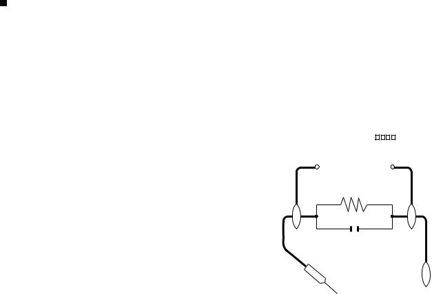
•Plug the AC cord directly into a 110 ~ 240 volt AC outlet.
•Using two clip leads, connect a 1.5k ohm, 10 watt resistor paralleled by a 0.15µF capacitor in series with all exposed metal cabinet parts and a known earth ground, such as electrical conduit or electrical ground connected to an earth ground.
•Use an AC voltmeter having with 5000 ohm per volt, or higher, sensitivity or measure the AC voltage drop across the resistor.
0.15 µF
TEST PROBE
TO EXPOSED |
CONNECT TO |
METAL PARTS |
KNOWN EARTH |
|
GROUND |
///////////////////////////////////////////////////////////////////////////////////////////////////////////////////////////////////////////////////////////////////////////////////////////////////////////////////////////////////////////
SAFETY NOTICE
Many electrical and mechanical parts in LCD color television have special safety-related characteristics.
These characteristics are often not evident from visual inspection, nor can protection afforded by them be necessarily increased by using replacement components rated for higher voltage, wattage, etc.
Replacement parts which have these special safety characteristics are identified in this manual; electrical components having such features
are identified by " " and shaded areas in the Replacement Parts Lists and Schematic Diagrams.
For continued protection, replacement parts must be identical to those used in the original circuit.
The use of a substitute replacement parts which do not have the same safety characteristics as the factory recommended replacement parts shown in this service manual, may create shock, fire or other hazards.
///////////////////////////////////////////////////////////////////////////////////////////////////////////////////////////////////////////////////////////////////////////////////////////////////////////////////////////////////////////
v
LC-32PX5M/X/LC-37PX5M/X
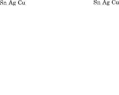
Precautions for using lead-free solder
Employing lead-free solder
•“All PWBs” of this model employs lead-free solder. The LF symbol indicates lead-free solder, and is attached on the PWBs and service manuals. The alphabetical character following LF shows the type of lead-free solder.
Example:
L |
F |
a |
L |
F |
a/a |
||||
|
|
|
|
|
|
|
|
|
|
Indicates lead-free solder of tin, silver and copper.
Indicates lead-free solder of tin, silver and copper.
Using lead-free wire solder
•When fixing the PWB soldered with the lead-free solder, apply lead-free wire solder. Repairing with conventional lead wire solder may cause damage or accident due to cracks.
As the melting point of lead-free solder (Sn-Ag-Cu) is higher than the lead wire solder by 40 °C, we recommend you to use a dedicated soldering bit, if you are not familiar with how to obtain lead-free wire solder or soldering bit, contact our service station or service branch in your area.
Soldering
•As the melting point of lead-free solder (Sn-Ag-Cu) is about 220 °C which is higher than the conventional lead solder by 40 °C, and as it has poor solder wettability, you may be apt to keep the soldering bit in contact with the PWB for extended period of time. However, Since the land may be peeled off or the maximum heat-resistance temperature of parts may be exceeded, remove the bit from the PWB as soon as you confirm the steady soldering condition.
Lead-free solder contains more tin, and the end of the soldering bit may be easily corroded. Make sure to turn on and off the power of the bit as required.
If a different type of solder stays on the tip of the soldering bit, it is alloyed with lead-free solder. Clean the bit after every use of it. When the tip of the soldering bit is blackened during use, file it with steel wool or fine sandpaper.
•Be careful when replacing parts with polarity indication on the PWB silk.
Lead-free wire solder for servicing
Part No. |
|
|
Description |
Code |
|
ZHNDAi123250E |
J |
φ0.3mm 250g |
(1roll) |
BL |
|
ZHNDAi126500E |
J |
φ0.6mm |
500g |
(1roll) |
BK |
ZHNDAi12801KE |
J |
φ1.0mm |
1kg (1roll) |
BM |
|
vi
Item |
|
|
|
LC-32PX5M/X |
|
|
LC-37PX5M/X |
|
|
|
|
|
|
||||
|
|
|
|
|
|
|
|
|
LCD panel |
|
|
|
32 (80 cm) Advanced |
|
|
37 (94 cm) Advanced |
|
|
|
|
|
Super View & BLACK TFT |
|
|
Super View & BLACK TFT |
|
|
|
|
|
LCD |
|
|
|
LCD |
|
|
|
|
|
|
|
|
|
Number of dots |
3,147,264 dots (1366 768 3 dots) |
|
||||||
Video Colour System |
PAL/SECAM/NTSC 3.58/NTSC 4.43/PAL 60 |
|||||||
TV |
TV-Standard |
PAL: B/G, D/K, I SECAM: B/G, D/K, K/K1 |
NTSC: M |
|||||
Function |
Receiving VHF/UHF |
44.25—863.25 MHz |
|
|||||
|
|
|||||||
|
Channel |
S1—S41ch (including Hyperband) |
|
|||||
|
|
|
CATV |
|
||||
|
TV-Tuning System |
Auto Preset 99 ch |
|
|||||
|
STEREO/BILINGUAL |
NICAM: B/G, I, D/K A2 stereo: B/G |
|
|||||
Brightness |
|
|
|
450 cd/m2 |
|
|||
Viewing angles |
H : 176º V : 176º |
|
||||||
|
|
|
|
|
|
|
|
|
|
|
|
|
10W |
2 |
|
|
|
|
|
|
|
|
|
|
||
|
|
|
|
|
|
|
||
Speakers |
|
|
|
10 |
4 cm 2pcs, Ø 2 cm 2pcs |
|
||
|
|
|
|
|
||||
Terminals |
Rear |
|
ANTENNA IN |
UHF/VHF 75 DIN type |
|
|||
|
|
|
INPUT 1 |
VIDEO in, AUDIO in, |
|
|||
|
|
|
|
COMPONENT in (480I, 576I, 480P, 576P, 720P/60Hz, 1080I/50Hz, 1080I/60Hz) |
||||
|
|
|
INPUT 2 |
VIDEO in, AUDIO in, |
|
|||
|
|
|
|
COMPONENT in (480I, 576I, 480P, 576P, 720P/60Hz, 1080I/50Hz, 1080I/60Hz) |
||||
|
|
|
INPUT 3 |
HDMI (HDMI input) (480P, 576P, 720P/60Hz, 1080I/50Hz, 1080I/60Hz), AUDIO in |
||||
|
|
|
INPUT 4 |
HDMI (HDMI input) (480P, 576P, 720P/60Hz, 1080I/50Hz, 1080I/60Hz) |
||||
|
|
|
PC INPUT |
15 pin mini D-sub, AUDIO in (Ø 3.5mm jack) |
||||
|
|
|
MONITOR OUTPUT |
VIDEO out, AUDIO out |
|
|||
|
|
|
RS-232C |
9 pin D-sub male connector |
|
|||
|
|
|
|
|
||||
OSD language |
English/Chinese/Arabic |
|
||||||
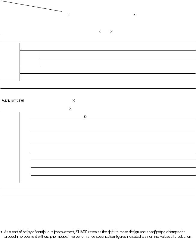
Power Requirement |
AC 110—240 V, 50/60 Hz |
|
||||||
Power Consumption |
|
|
|
|
||||
158 W (0.8 W Standby) |
|
171 W (0.8 W Standby) |
||||||
|
|
|
|
|
|
|
||
Weight |
|
|
without stand |
16.5 kg |
|
20.3 kg |
||
|
|
|
|
|
|
|
|
|
|
|
with stand |
18.4 kg |
|
22.9 kg |
|||
|
|
|
|
|||||
|
|
|
|
|
|
|
|
|
Operating Temperature |
0°C — 40°C |
|
||||||
|
|
|
|
|
|
|
|
|
units. There may be some deviations from these values in individual units.
1 – 1

LC-32PX5M/X/LC-37PX5M/X
CHAPTER 2. OPERATION MANUAL
[1] OPERATION MANUAL
Part names
TV (Front)
Channel up ( )/down ( ) buttons |
|
|
|
|
|
|
TV/VIDEO button |
||||||||||
Volume up ( )/down ( |
|
) buttons |
|
|
|
|
|
|
|
|
POWER (On/Off) button |
||||||
|
|
|
|
|
|
|
|
|
|
|
|
|
|
|
|
|
|
|
|
|
|
|
|
|
|
|
|
|
|
|
|
|
|
|
|
|
|
|
|
|
|
|
|
|
|
|
|
|
|
|
|
|
|
Remote control sensor |
|
|
|
|
|
|
|
OPC indicator* |
|
|
|
|
|
|
|
||||
OPC sensor |
|
|
|
|
SLEEP timer indicator |
||||
|
|
|
|
||||||
|
|
|
|
|
|
|
|
|
*OPC: Optical Picture Control |
|
|
|
POWER indicator |
|
|
||||
2 – 1

LC-32PX5M/X/LC-37PX5M/X
Part names
TV (Rear)
RS-232C terminal
PC INPUT terminals
INPUT 4 (HDMI) terminal
INPUT 3 (HDMI) terminals
INPUT 1 terminals
INPUT 2 terminals
MONITOR OUTPUT terminals
Antenna input terminal |
AC INPUT terminal |
|
2 – 2
LC-32PX5M/X/LC-37PX5M/X
Part names
Remote control unit
(TELETEXT)
Select the TELETEXT mode. (all TV image, all TEXT image, TV/TEXT image)
POWER (STANDBY/ON)
To switch the power on and off.
(Hold)
TELETEXT mode: Stop updating Teletext pages automatically. Press
again to release the hold mode.
0 — 9
Set the channel.
TELETEXT mode: Set the page.
(Flashback)
Press to return to the previous channel or external input mode.
WIDE
Change the wide image mode.
AV MODE
Select a video setting: AV MODE (STANDARD, MOVIE, GAME, USER, DYNAMIC, DYNAMIC (FIXED)), PC MODE (STANDARD, USER)
MPX
Select the sound multiplex mode.
VOL /VOL
Set the volume.
(Mute)
Mute the sound.
P&P
Set the dual picture mode. Press P&P again to return to normal view.
SURROUND
Select Surround settings.
// / (Cursor)
Select a desired item on the setting screen.
EXIT
Return to the default screen.
 NOTE
NOTE
• When using the remote control unit, point it at the TV.
(Reveal hidden for TELETEXT)
TELETEXT mode: Display hidden characters.
(SUBTITLE for TELETEXT)
To turn the subtitles on and off.
(Top/Bottom/Full)
TELETEXT mode: Set the area of
(Subpage)
Display the Teletext subpage directly.
TV/VIDEO (INPUT SOURCE)
Select an input source. (TV, INPUT 1, INPUT 2, INPUT 3, INPUT 4, PC)
OPC
To switch Optical Picture Control on and off.
FREEZE
Freeze a motion picture on the screen.
DISPLAY
Display the channel and input source.
CH /CH
TV input mode: Select the channel. TELETEXT mode: Select the page.
SLEEP
Set the Sleep timer.
SELECT
To select either screen to be active in Dual screen mode.
MENU
Display the menu screen.
ENTER
Execute a command.
RETURN
MENU mode: Return to the previous menu screen.
Colour (Red/Green/Yellow/ Blue)
TELETEXT mode: Select a page.
2 – 3
LC-32PX5M/X/LC-37PX5M/X
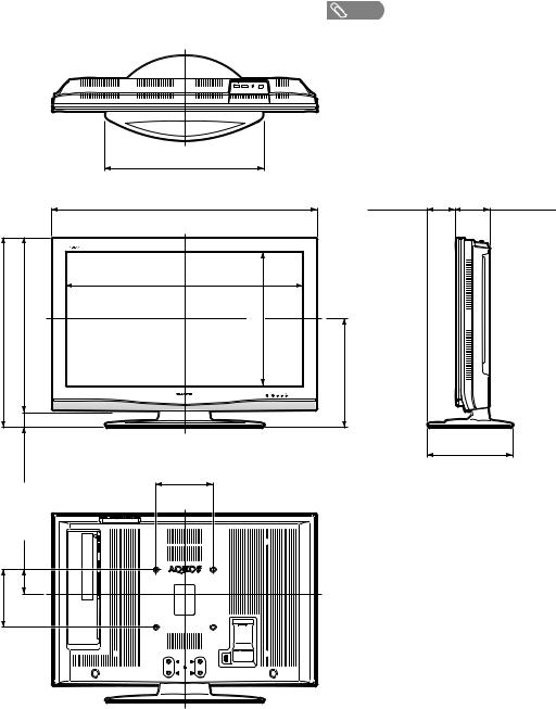
CHAPTER 3. DIMENSIONS
[1] DIMENSIONS
LC-32PX5M/X, LC-37PX5M/X |
|
Unit: mm |
||
|
|
|
NOTE |
|
|
|
• |
Figures within parentheses are for LC-37PX5M/X. |
|
|
|
506 (542) |
|
|
|
|
797 (920) |
100 (84) |
116 (116) |
|
|
700.4 (823) |
|
|
590.5 (657) |
533 (600) |
395.1 (464) |
(377) |
|
|
|
|
343 |
|
|
(57)57.5 |
200 (200) |
|
250 (292) |
|
|
|
|
|
|
85 (85) |
|
|
|
200 (200) |
|
|
|
|
3 – 1
LC-32PX5M/X/LC-37PX5M/X
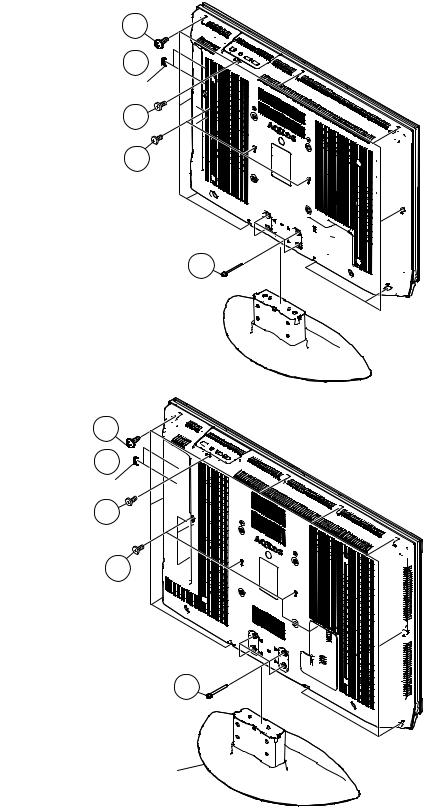
CHAPTER 4. REMOVING OF MAJOR PARTS
[1] REMOVING OF MAJOR PARTS
1.Detach the 2 BUS Covers [1].
2.Remove the 4 screws [2] and detach the Stand.
3.Remove the 1 screw [3], 4 (32PX5M/X)/6 (37PX5M/X) screws [4] and the 9 (32PX5M/X)/10 (37PX5M/X) screws [5]. Detach the Rear Cabinet.
(LC-32PX5M/X)
5
1
BUS Cover
3
4
2
Stand 
(LC-37PX5M/X)
5
1
BUS Cover
3
4
2
Stand
4 – 1

LC-32PX5M/X/LC-37PX5M/X
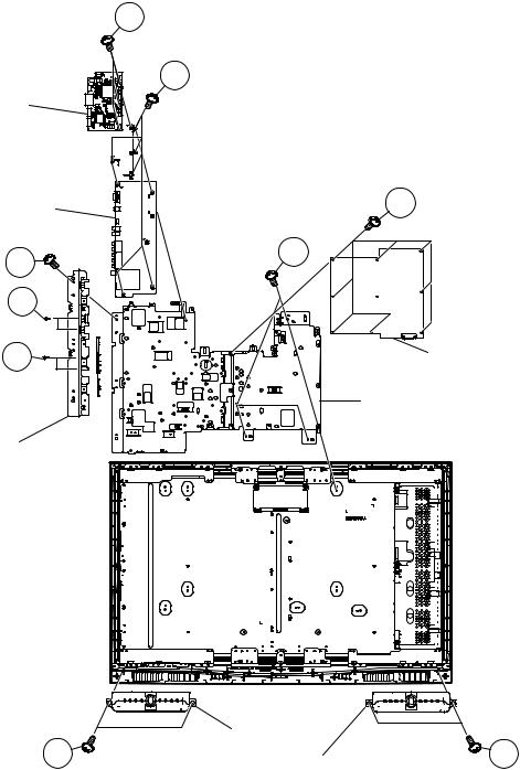
4.Remove the 4 screws [6] and detach the Support Angle.
5.Remove the 3 screws [7] and the Bottom Cover.
6.Remove the 2 (32PX5M/X)/4 (37PX5M/X) screws [8] and detach the Stand Angle.
7.Remove the 6 (32PX5M/X)/4 (37PX5M/X) screws [9]. Detach the SUS Angle-L and SUS Angle-R.
8.Remove the 2 screws [10] and detach the Top Control Cover Ass'y.
Remove the 2 screws [11] , 1 screw [11A] and detach the OPERATION PWB Unit from Top Control Cover Ass'y.
(LC-32PX5M/X) |
9 |
|
|
Center Angle-R |
Center Angle-L |
6Support Angle
9
10 |
|
|
|
Top Control |
|
Cover Ass'y |
|
|
|
|
OPERATION |
11A |
|
PWB Unit |
|
|
11 |
|
|
|
|
|
|
|
|
|
|
|
|
Stand Angle |
Bottom Cover |
|
8
7
4 – 2

LC-32PX5M/X/LC-37PX5M/X
(LC-37PX5M/X) |
9 |
|
Center Angle-R |
Center Angle-L |
6Support Angle
10 |
9 |
Top Control
Cover Ass'y 
OPERATION 
PWB Unit
11
|
|
11A |
|
Bottom Cover
Stand Angle
8
7
4 – 3

LC-32PX5M/X/LC-37PX5M/X
9. Remove all the connectors [12] from all the PWBs.
(LC-32PX5M/X)


|
|
|
12 |
|
|
|
||
|
||
|
|
12
(LC-37PX5M/X)


12
|
|
|
|
|
|
|
|
|
|
|
|
|
|
|
12 |
|
|
|
|
|
|
|
|
|
|
12 |
|
|
12
4 – 4

LC-32PX5M/X/LC-37PX5M/X
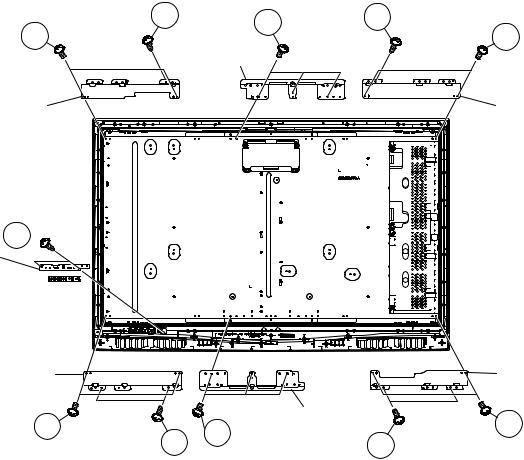
10.Remove the 2 (32PX5M/X)/4 (37PX5M/X) screws [13]. Detach the Speaker Box L and Speaker Box R. 11.Remove the 5 (32PX5M/X)/4 (37PX5M/X) screws [14] and detach Chassis Tray.
12.Remove the 2 screws [16] and 2 screws [17]. Detach the AV Terminal Cover.
13.Remove the 8 screws [18] and detach the POWER PWB Unit from Chassis Tray. 14.Remove the 6 screws [19] and detach the SUB PWB Unit from Chassis Tray. 15.Remove the 3 screws [20] and detach the MAIN PWB Unit from SUB PWB Unit.
(LC-32PX5M/X)
20
19
MAIN PWB Unit
SUB PWB Unit |
18 |
14
14 

17
16 |
POWER PWB Unit |
Chassis Tray
AV Terminal Cover
14 
Speaker Box R |
13 |
Speaker Box L |
13 |
|
4 – 5
LC-32PX5M/X/LC-37PX5M/X
(LC-37PX5M/X)
20
19
MAIN PWB Unit
SUB PWB Unit |
18 |
14 |
14 |
|
|
17 |
|
16 |
POWER PWB Unit |
|
Chassis Tray |
AV Terminal Cover |
|
|
Speaker Box R |
|
13 |
Speaker Box L |
13 |
|
|
4 – 6

LC-32PX5M/X/LC-37PX5M/X
16.Remove the 7 (32PX5M/X)/6 (37PX5M/X) screws [21] and take out the LCD Panel from Front Cabinet. 17.Remove the 9 (32PX5M/X)/14 (37PX5M/X) screws [22] and detach the LCD Angles.
18.Remove the 2 screws [24] and detach the LED, R/C PWB Unit.
(LC-32PX5M/X)
21 |
LCD Angle Top R |
21 |
|
22 |
22 |
||
|
LCD Angle Top L
24
LED, R/C
PWB Unit
LED Cover 
LCD Angle |
|
LCD Angle |
|
Bottom R |
|
||
LCD Angle |
Bottom R |
||
|
|||
22 |
Bottom C |
|
|
|
22 |
||
22 |
|
||
21 |
21 |
21 |
4 – 7
LC-32PX5M/X/LC-37PX5M/X
(LC-37PX5M/X) |
|
|
|
21 |
22 |
21 |
|
22 |
22 |
||
LCD Angle |
|||
|
|
||
|
Top C |
|
|
LCD Angle Top R |
|
LCD Angle Top L |
24 
LED, R/C
PWB Unit
LED Cover 
LCD Angle |
|
|
LCD Angle |
Bottom L |
|
|
|
|
|
Bottom R |
|
|
|
|
|
|
|
LCD Angle |
|
22 |
|
Bottom C |
22 |
22 |
|
||
21 |
|
21 |
|
|
|
4 – 8
LC-32PX5M/X/LC-37PX5M/X
- M E M O -
4 – 9
LC-32PX5M/X/LC-37PX5M/X
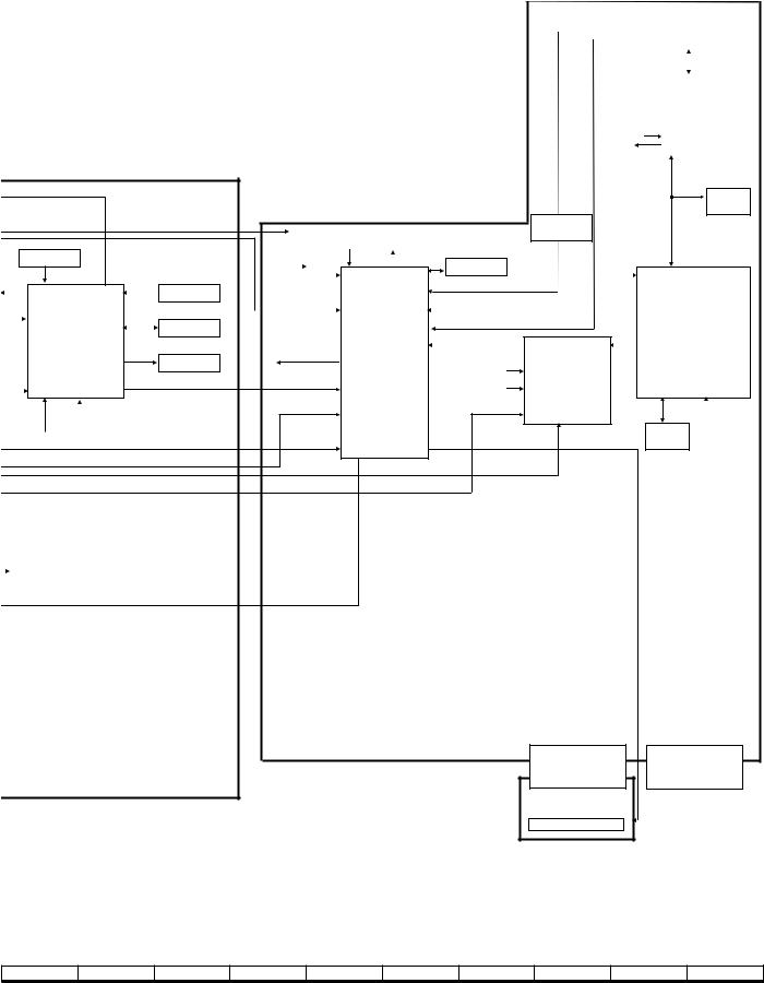
CHAPTER 5. BLOCK DIAGRAM/OVERALL WIRING DIAGRAM
[1] BLOCK DIAGRAM
|
|
|
|
|
|
|
|
|
|
|
|
|
|
|
|
|
|
|
|
|
|
|
|
|
|
|
|
|
|
|
|
|
|
|
|
|
||
|
|
|
|
|
|
|
|
|
|
|
|
|
|
|
|
|
|
|
|
|
|
|
|
|
|
J |
|
|
|
|
|
|
|
|
|
|
||
|
|
|
|
|
|
|
|
|
|
|
|
|
|
|
|
|
|
|
|||||||
|
|
|
|
|
|
|
|
|
|
|
||
|
|
|
|
|
|
|
|
|
|
|
||
|
|
|
|
|
|
|
|
|
|
|
|
|
|
|
|
|
|
|
|
|
|
|
|
||
|
|
|
|
|
|
|
|
|
|
|
||
|
|
|
|
|
|
|
|
|
||||
|
|
|
|
|
|
|
|
|
|
|
|
|
I |
|
|
|
|
|
|
|
|
||||
|
|
|
|
|
|
|
|
|
|
|
|
|
|
|
|
|
|
|
|
|
|
|
|
|
|
|
|
|
|
|
|
|
|
|
|
|
|
|
|
|
|
|
|
|
|
|
|
|
|
|
|
|
|
|
|
|
|
|
|
|
|
|
|
|
|
|
|
|
|
|
|
|
|
|
|
|
|
H |
|
|
|
|
|
|
|
|
|
|
|
|
|
|
|
|
|
|
|
|
|
|
|
||
|
|
|
|
|
|
|
|
|
|
|
|
|
|
|
|
|
|
|
|
|
|
|
|
||
|
|
|
|
|
|
|
|
|
|
|
|
|
|
|
|
|
|
|
|
|
|
|
|
|
|
|
|
|
|
|
|
|
|
|
|
|
|
|
|
|
|
|
|
|
|
|
|
|
|
||
|
|
|
|
|
|
|
|
|
|
|
||
|
|
|
|
|
|
|
|
|
|
|
||
|
|
|
|
|
|
|
|
|
|
|||
|
|
|
|
|
|
|
|
|
|
|||
|
|
|
|
|
|
|
|
|
|
|
||
|
|
|
|
|
|
|
|
|
||||
G |
|
|
|
|
|
|
|
|
|
|
|
|
|
|
|
|
|
|
|
|
|
|
|
||
|
|
|
|
|
|
|
|
|
|
|
||
|
|
|
|
|
|
|
|
|
|
|
|
|
|
|
|
|
|
|
|
|
|
|
|
|
|
|
|
|
|
|
|
|
|
|
|
|
|
|
|
|
|
|
|
|
|
|
|
|
|
|
|
|
|
|
|
|
|
|
|
|
|
|
|
|
|
|
|
|
|
|
|
|
|
|
|
|
|
F |
|
|
|
|
|
|
|
|
|
|
|
|
|
|
|
|
|
|
|
|
|
|
|
|
|
|
|
|
|
|
|
|
|
|
|
|
|
|
|
|
|
|
|
|
|
|
|
|
|||
|
|
|
|
|
|
|
|
|||||
|
|
|
|
|
|
|
|
|
|
|
||
|
|
|
|
|
|
|
|
|
|
|
|
|
|
|
|
|
|
|
|
|
|
|
|
||
|
|
|
|
|
|
|
|
|
||||
|
|
|
|
|
|
|
|
|
|
|
||
|
|
|
|
|
|
|
|
|
|
|
||
|
|
|
|
|
|
|
|
|
|
|
|
|
|
|
|
|
|
|
|
|
|
|
|
|
|
E |
|
|
|
|
|
|
|
|
|
|
|
|
|
|
|
|
|
|
|
|
|
|
|
|
|
|
|
|
|
|
|
|
|
|
|
|
||
|
|
|
|
|
|
|
|
|
|
|
|
|
|
|
|
|
|
|
|
|
|
|
|
|
|
|
|
|
|
|
|
|
|
|
|
|
|
|
|
|
|
|
|
|
|
|
|
|
|
||
|
|
|
|
|
|
|
|
|
|
|
|
|
|
|
|
|
|
|
|
|
|
|
|
|
|
|
|
|
|
|
|
|
|
|
|
|
|
|
|
|
|
|
|
|
|
|
|
|
|||
|
|
|
|
|
|
|
|
|
|
|||
|
|
|
|
|
|
|
||||||
|
|
|
|
|
|
|
|
|
|
|
|
|
|
|
|
|
|
|
|
|
|
|
|
|
|
D |
|
|
|
|
|
|
|
|
|
|
|
|
|
|
|
|
|
|
|
|
|
|
|
|
|
|
|
|
|
|
|
|
|
|
|
|
|
|
|
|
|
|
|
|
|
|
|
|
|
|
|
|
|
|
|
|
|
|
|
|
|
|
|
|
C |
|
|
|
|
|
|
|
|
|
|
|
|
|
|
|
|
|
|
|
|
|
|
|
|
|
|
|
|
|
|
|
|
|
|
|
|
||
|
|
|
|
|
|
|
|
|
|
|||
|
|
|
|
|
|
|
|
|
|
|
|
|
|
|
|
|
|
|
|
|
|
|
|
|
|
|
|
|
|
|
|
|
|
|
|
|
||
B |
|
|
|
|
|
|
|
|
|
|
|
|
|
|
|
|
|
|
|
|
|
|
|
||
|
|
|
|
|
|
|
|
|
|
|
||
A |
|
|
|
|
|
|
|
|
|
|
|
|
1 |
2 |
3 |
4 |
5 |
6 |
|
|
7 |
8 |
9 |
|
10 |
|
|
|
|
|
5 – 1 |
|
|
|
|
|
|
|
LC-32PX5M/X/LC-37PX5M/X
|
|
|
|
|
|
|||
|
|
|
|
|||||
|
|
|
|
|
|
|
||
|
|
|
|
|
||||
|
|
|
|
|
|
|||
|
|
|
|
|
|
|
||
|
|
|
|
|
|
|
|
|
|
|
|
|
|
|
|
|
|
|
|
|
|
|
|
|
|
|
|
|
|
|
|
|
|
|
|
|
|
|
|
|
|
|
||
|
|
|
|
|
|
|||
|
|
|
|
|
|
|
||
|
|
|
|
|
|
|
|
|
|
|
|
|
|
|
|
|
|
|
|
|
|
|
|
|
|
|
|
|
|
|
|
|
|
|
|
|
|
|
|
|
|
|
|
|
|
|
|
|
|
|
|
|
|
|
|
|
|
|
|
|
|
|
|
|
|
|
|
|
|
|
|
|
|
|
|
|
|
|
|
|
|
|
|
|
|
|
|
|
|
|
|
|
|
|
||
|
|
|
|
|
|
|
|
|||
|
|
|
|
|
|
|
|
|||
|
|
|
|
|
|
|
|
|
||
|
|
|
|
|
|
|
|
|
|
|
|
|
|
|
|
|
|
|
|
|
|
|
|
|
|
|
|
|
|
|
|
|
|
|
|
|
|
|
|
|
|
||
|
|
|
|
|
|
|
|
|
|
|
|
|
|
|
|
|
|
|
|
|
|
|
|
|
|
|
|
|
|
|
|
|
|
|
|
|
|
|
|
|
|
|
|
|
|
|
|
|
|
|
|
|
||
|
|
|
|
|
|
|
|
|
|
|
|
|
|
|
|
|
|
|
|
|
|
|
|
|
|
|
|
|
|
|
||
|
|
|
|
|
|
|
|
|
||
|
|
|
|
|
|
|
|
|
||
|
|
|
|
|
|
|
||||
|
|
|
|
|
|
|
|
|
|
|
|
|
|
|
|
|
|
|
|
|
|
|
|
|
|
|
|
|
|
|
|
|
|
|
|
|
|
|
|
|
|
|
|
|
|
|
|
|
|
|
|
|
|
|
|
|
|
|
|
|
|
|
|
|
|
|
|
|
|
|
|
|
|
|
|
|
|
|
|
|
|
|
|
|
|
|
|
|
|
|
|
|
|
|
|
|
|
|
|
|
|
|
|
|
|
|
|
|
|
|
|
|
|
|
|
|
|
|
|
|
|
|
|
|
|
|
|
|
|
|
|
|
|
|
|
|
|
|
|
|
|
|
|
|
|
|
|
|
|
|
|
||
|
|
|
|
|
|
|
|
|
|
|
|
|
|
|
|
|
|
|
|||
|
|
|
|
|
|
|
|
|
|
|
|
|
|
|
|
|
|
|
|
|
|
|
|
|
|
|
|
|
|
|
|
|
10 |
11 |
12 |
13 |
14 |
15 |
16 |
17 |
18 |
|
19 |
|
|
|
|
|
5 – 2 |
|
|
|
|
|
LC-32PX5M/X/LC-37PX5M/X
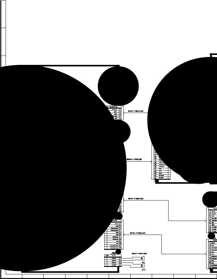
[2] OVERALL WIRING DIAGRAM (LC-32PX5M/X)
J |
|
|
|
|
|
|
|
|
|
I |
|
|
|
|
|
|
|
|
|
H |
|
|
|
|
|
|
|
|
|
G |
|
|
|
|
|
|
|
|
|
F |
|
|
|
|
|
|
|
|
|
E |
|
|
|
|
|
|
|
|
|
D |
|
|
|
|
|
|
|
|
|
C |
|
|
|
|
|
|
|
|
|
B |
|
|
|
|
|
|
|
|
|
A |
|
|
|
|
|
|
|
|
|
1 |
2 |
3 |
4 |
5 |
6 |
7 |
8 |
9 |
10 |
|
|
|
|
|
5 – 3 |
|
|
|
|
 Loading...