


Samsung S6B1713A11-xxXN, S6B1713A01-B0CZ, S6B1713A01-xxX0, S6B1713A01-xxXN, S6B1713A11-B0CY Datasheet
...S6B1713
65 COM / 132 SEG DRIVER & CONTROLLER FOR STN LCD
January.2000
Ver. 4.0
Prepared by:  Jae-Su, Ko
Ko1942@samsung.co.kr
Contents in this document are subject to change without notice. No part of this document may be reproduced or transmitted in any form or by any means, electronic or mechanical, for any purpose, without the express written permission of LCD Driver IC Team.

65 COM / 132 SEG DRIVER & CONTROLLER FOR STN LCD |
S6B1713 |
|
|
S6B1713 Specification Revision History
Version |
Content |
Date |
|
|
|
|
|
2.0 |
Neglect the more past version than version 2.0 |
Nov.1998 |
|
|
|
|
|
2.1 |
fOSC = 16kHz (Typ.) → 22kHz (Typ.): For removing flicker phenomenon |
Nov.1998 |
|
Temperature coefficient (when TEMPS = L): -0.0%/°C → -0.05%/°C |
|||
|
|
||
|
|
|
|
|
Modified some syntax errors |
|
|
3.0 |
Voltage regulator reference voltage [VREF]: TBD → 2.0 |
Nov.1998 |
|
|
Modified voltage regulator block of “Functional Description” |
|
|
|
|
|
|
3.1 |
VLCD absolute maximum rating: 15.0V → 17.0V |
|
|
Power consumption: 100μA → 80μA |
|
||
|
|
||
|
|
|
|
3.2 |
Oscillator frequency (1): 19 (Min.) →17 (Min.), 25 (Max.) →27 (Max.) |
|
|
Oscillator frequency (2): 22 (Min.) →20 (Min.), 28 (Max.) →30 (Max.) |
|
||
|
|
||
|
|
|
|
3.3 |
Modified Y-axis values of “Pad Center Coordinates” |
|
|
Modified the contents of “Referential Instruction Setup Flow” |
|
||
|
|
||
|
|
|
|
3.4 |
Word-processor version change |
Apr.1999 |
|
|
|
|
|
3.5 |
Modified error: pad No.113 (COMS) Y Coordinate: -1210 → -1140 (after) |
Oct.1999 |
|
|
|
|
|
4.0 |
Change VDD Range : 2.4V to 5.5V → 2.4V to 3.6V |
Jan.2000 |
|
|
|
|
2

S6B1713 |
65 COM / 132 SEG DRIVER & CONTROLLER FOR STN LCD |
|
|
CONTENTS |
|
INTRODUCTION.................................................................................................................................................. |
1 |
FEATURES ......................................................................................................................................................... |
1 |
BLOCK DIAGRAM .............................................................................................................................................. |
3 |
PAD CONFIGURATION....................................................................................................................................... |
4 |
PAD CENTER COORDINATES ........................................................................................................................... |
5 |
PIN DESCRIPTION.............................................................................................................................................. |
8 |
POWER SUPPLY ......................................................................................................................................... |
8 |
LCD DRIVER SUPPLY ................................................................................................................................. |
8 |
SYSTEM CONTROL .................................................................................................................................... |
9 |
MICROPROCESSOR INTERFACE ............................................................................................................. |
11 |
LCD DRIVER OUTPUTS ............................................................................................................................. |
13 |
FUNCTIONAL DESCRIPTION............................................................................................................................ |
14 |
MICROPROCESSOR INTERFACE ............................................................................................................. |
14 |
DISPLAY DATA RAM (DDRAM) .................................................................................................................. |
18 |
LCD DISPLAY CIRCUITS............................................................................................................................ |
21 |
LCD DRIVER CIRCUIT................................................................................................................................ |
23 |
POWER SUPPLY CIRCUITS....................................................................................................................... |
24 |
REFERECE CIRCUIT EXAMPLES .............................................................................................................. |
31 |
RESET CIRCUIT ......................................................................................................................................... |
33 |
INSTRUCTION DESCRIPTION........................................................................................................................... |
34 |
SPECIFICATIONS .............................................................................................................................................. |
48 |
ABSOLUTE MAXIMUM RATINGS ............................................................................................................... |
48 |
DC CHARACTERISTICS ............................................................................................................................. |
49 |
REFERENCE DATA .................................................................................................................................... |
52 |
AC CHARACTERISTICS ............................................................................................................................. |
54 |
REFERENCE APPLICATIONS........................................................................................................................... |
58 |
MICROPROCESSOR INTERFACE ............................................................................................................. |
58 |
CONNECTIONS BETWEEN S6B1713 AND LCD PANEL ............................................................................ |
59 |
TCP PIN LAYOUT (SAMPLE)...................................................................................................................... |
64 |
3

S6B1713 |
65 COM / 132 SEG DRIVER & CONTROLLER FOR STN LCD |
|
|
INTRODUCTION
The S6B1713 is a driver & controller LSI for graphic dot-matrix liquid crystal display systems. It contains 65 commons and 132 segments driver circuits. This chip is connected directly to a microprocessor, accepts serial or 8-bit parallel display data and stores in an on-chip Display Data RAM of 65 x 132 bits. It provides a high-flexible display section due to 1-to-1 correspondence between on-chip display data RAM bits and LCD panel pixels. And it performs display data RAM read/write operation with no externally operating clock to minimize power consumption. In addition, because it contains power supply circuits necessary to drive liquid crystal, it is possible to make a display system with the fewest components.
FEATURES
Driver Output Circuits
−65 common outputs / 132 segment outputs
On-chip Display Data RAM
−Capacity: 65 x 132 = 8,580 bits
Applicable Duty Ratios
Duty ratio |
Applicable LCD bias |
Maximum display area |
|
|
|
1/65 |
1/7 or 1/9 |
65 × 132 |
|
|
|
1/49 |
1/6 or 1/8 |
49 × 132 |
|
|
|
1/33 |
1/5 or 1/6 |
33 × 132 |
|
|
|
Microprocessor Interface
−8-bit parallel bi-directional interface with 6800-series or 8080-series
−Serial interface (only write operation) available
Function Set
−Various instructions sets
−H/W, S/W reset capable
Built-in Analog Circuit
−On-chip oscillator circuit
−Voltage converter (x2, x3, x4, x5)
−Voltage regulator (temperature coefficient: -0.05%/°C, -0.2%/°C)
−Voltage follower
−Electronic contrast control function (64 steps)
Operating Voltage Range
−Supply voltage (VDD): 2.4 to 3.6 V
−LCD driving voltage (VLCD = V0 - VSS): 4.0 to 15.0 V
Low Power Consumption
−70 μΑ Typ. (VDD = 3V, x4 boosting, V0 = 11V, internal power supply ON)
−10 μΑ Max. (during power save [standby] mode)
Package Type
−Gold bumped chip or TCP
1

65 COM / 132 SEG DRIVER & CONTROLLER FOR STN LCD |
S6B1713 |
|
|
Series Specifications
Product code |
TEMPS pin |
Temp. coefficient |
Package |
Chip thickness |
|
|
|
|
|
|
|
S6B1713A01-B0CZ |
0 |
-0.05%/°C |
|
670 μm |
|
S6B1713A01-B0CY |
(VSS connected) |
|
470 μm |
||
|
|
||||
|
|
COG |
|||
|
|
|
|
||
S6B1713A11-B0CZ |
1 |
-0.2%/°C |
670 μm |
||
|
|||||
S6B1713A11-B0CY |
(VDD connected) |
|
470 μm |
||
|
|
||||
|
|
|
|||
|
|
|
|
|
|
S6B1713A01-xxX0 |
0 |
-0.05%/°C |
|
670 μm |
|
S6B1713A01-xxXN |
(VSS connected) |
|
470 μm |
||
|
|
||||
|
|
TCP |
|||
|
|
|
|
||
S6B1713A11-xxX0 |
1 |
-0.2%/°C |
670 μm |
||
|
|||||
S6B1713A11-xxXN |
(VDD connected) |
|
470 μm |
||
|
|
||||
|
|
|
|||
|
|
|
|
|
* xx: TCP ordering number
2

S6B1713 |
65 COM / 132 SEG DRIVER & CONTROLLER FOR STN LCD |
|
|
BLOCK DIAGRAM
|
|
COMS |
COM1 |
COM32 : |
SEG3 SEG2 SEG1 |
: |
SEG131 SEG130 : |
SEG132 |
COMS COM64 : COM33 |
|
VDD |
|
|
|
|
|
|
|
|
|
|
V0 |
|
|
|
|
|
|
|
|
|
|
V1 |
|
33 COMMON |
132 SEGMENT |
|
33 COMMON |
|
||||
V2 |
|
|
|
|||||||
|
DRIVER |
DRIVER CIRCUITS |
|
DRIVER |
|
|||||
V3 |
|
|
|
|||||||
|
CIRCUITS |
|
|
|
|
CIRCUITS |
|
|||
V4 |
|
|
|
|
|
|
||||
|
|
|
|
|
|
|
|
|
|
|
VSS |
|
|
|
|
|
|
|
|
|
|
|
|
|
SEGMENT CONTROLLER |
COMMON CONTROLLER |
|
|||||
|
V / F |
|
|
|
|
|
|
|
|
|
HPMB |
CIRCUIT |
|
|
|
|
|
|
|
|
|
|
|
|
|
|
|
|
|
|
|
MS |
V0 |
PAGE |
I/O |
|
DISPLAY DATA RAM |
LINE |
|
DISPLAY |
CL |
||
ADDRESS |
|
ADDRESS |
|
M |
||||||
BUFFER |
65 X 132 = 8,580 Bits |
|
TIMING |
|||||||
|
CIRCUIT |
CIRCUIT |
|
FRS |
||||||
|
|
|
|
|
|
|
GENERATOR |
|||
VR |
|
|
|
|
|
|
|
|
||
|
|
|
|
|
|
|
|
DISP |
||
|
|
|
|
|
|
|
|
CIRCUIT |
||
INTRS |
|
|
|
|
|
|
|
|
DUTY0 |
|
V / R |
|
|
|
|
|
|
|
|
||
TEMPS |
|
|
|
|
|
|
|
|
DUTY1 |
|
CIRCUIT |
|
|
|
|
|
|
|
|
||
|
|
|
COLUMN ADDRESS |
|
|
|
|
|||
|
|
|
|
|
|
|
|
|||
|
|
|
|
|
CIRCUIT |
|
|
|
|
|
VOUT |
|
|
|
|
|
|
|
|
OSCILLATOR |
CLS |
|
|
|
|
|
|
|
|
|
||
C1- |
|
|
|
|
|
|
|
|
|
|
C1+ |
|
|
|
|
|
|
|
|
|
|
C2- |
V / C |
|
|
|
|
|
|
|
|
|
C2+ |
|
|
|
|
|
|
|
|
|
|
CIRCUIT |
|
|
|
|
|
|
|
|
|
|
C3- |
|
STATUS REGISTER |
INSTRUCTION REGISTER |
|
||||||
|
|
|
||||||||
C3+ |
|
|
|
|||||||
|
|
|
|
|
|
|
|
|
|
|
DCDC5B |
|
|
|
|
|
|
|
|
|
|
BSTS |
|
|
|
BUS HOLDER |
|
INSTRUCTION DECODER |
|
|||
|
|
|
MPU INTERFACE (PARALLEL & SERIAL) |
|
||||||
|
|
CS1B |
CS2 |
RD E RS |
MI RESETB PS WR RW |
DB3 DB4 DB5 DB6(SCLK) DB7(SID) |
DB2 |
DB0 DB1 |
|
|
Figure 1. Block Diagram
3
65 COM / 132 SEG DRIVER & CONTROLLER FOR STN LCD |
S6B1713 |
|
|
PAD CONFIGURATION
|
|
287 |
148 |
|
|
|
288 |
-ðððð |
ррр ррррррррррррррррррр - - - - - - - - - - ррррррррррррррррррр ррр |
-ðððð |
147 |
||
Y |
|
|||||
|
|
|
||||
|
S6B1713 |
|
|
|||
|
- - |
|
- - |
|
||
|
(TOP VIEW) |
|
|
|||
|
- |
(0,0) |
X |
- |
|
|
|
ððð |
ððð |
|
|||
324 |
рррррррррррррррррррррр - - - - - - - - - - ррррррррррррррррррррррр |
111 |
||||
|
|
|||||
|
|
|
|
|||
|
|
1 |
110 |
|
|
|
Figure 2. S6B1713 Chip Configuration
Table 1. S6B1713 Pad Dimensions
Items |
Pad No. |
|
Size |
Unit |
|
|
|
|
|||
X |
|
Y |
|||
|
|
|
|
||
|
|
|
|
|
|
|
|
|
|
|
|
Chip size |
- |
10860 |
|
2920 |
|
|
|
|
|
|
|
Pad pitch |
1 to 110 |
|
90 |
|
|
|
|
|
|
|
|
111 to 324 |
|
70 |
|
||
|
|
|
|||
|
|
|
|
|
|
|
1 to 110 |
56 |
|
114 |
|
|
|
|
|
|
μm |
Bumped |
111 to 147 |
108 |
|
50 |
|
|
|
||||
pad size |
|
|
|
|
|
148 to 287 |
50 |
|
108 |
|
|
|
|
|
|
|
|
|
288 to 324 |
108 |
|
50 |
|
|
|
|
|
|
|
Bumped pad height |
1 to 324 |
17 (Typ.) |
|
||
|
|
|
|
|
|
COG Align Key Coordinate |
|
|
|
|
ILB Align Key Coordinate |
|
|
|
|
|||||||||||||||||||||||||||||
|
30μm 30μm 30μm |
|
|
|
|
|
30μm 30μm 30μm |
|
|
|
|
42μm |
108μm |
|
|
|
|
|
108μm |
42μm |
||||||||||||||||||
|
|
|
|
|
|
|
|
|
|
|
|
|
|
|
|
|
|
|
|
|
|
|
|
|
|
|
|
|
|
|
|
|
|
|
|
|
|
|
|
|
|
|
|
|
|
|
|
|
|
|
|
|
|
|
|
|
|
|
|
|
|
|
|
|
|
|
|
|
|
|
|
|
|
|
|
|
|
|
|
|
|
|
|
|
|
|
|
|
|
|
|
|
|
|
|
|
|
|
|
|
|
|
|
|
|
|
|
|
|
|
|
|
|
|
|
|
|
|
|
|
|
|
|
|
|
|
|
|
|
|
|
|
|
|
|
|
|
|
|
|
|
|
|
|
|
|
|
|
|
|
|
|
|
|
|
|
|
|
|
|
|
|
|
|
|
|
|
30 |
|
|
|
|
|
|
|
|
|
|
30 |
|
|
|
|
|
|
|
|
|
|
|
||||
|
|
|
|
|
|
|
|
|
|
|
|
|
|
μ |
(+5065, +1317) |
|
|
|
|
μ |
|
|
|
|
|
|
|
|
|
|
|
|||||||
|
|
|
|
|
|
|
|
|
|
|
|
|
|
m |
|
|
|
|
m |
|
|
|
|
|
108 |
|
|
|
|
|||||||||
|
|
|
|
|
|
|
|
|
|
|
|
|
|
|
|
|
|
|
|
|
|
|
|
|
|
|
|
|
|
|
|
|
|
|
|
|
||
|
(-5065, +1302) |
|
30 |
|
|
|
|
|
|
|
|
|
|
|
|
|
|
|
|
|
|
|
|
|
||||||||||||||
|
|
|
|
|
|
|
|
|
|
|
|
|
|
μ |
|
|
|
|
|
|
|
|
|
|
60 |
|
|
|
|
|
|
μ |
|
|
|
|
||
|
|
|
|
|
|
|
|
|
|
|
|
|
|
m |
|
|
|
|
|
|
|
|
|
|
|
|
|
|
||||||||||
|
|
|
|
|
|
|
|
|
|
|
|
|
30 |
|
|
|
|
|
|
|
|
|
|
|
|
μ |
|
|
|
|
|
|
m |
|
|
|
|
|
|
|
|
|
|
|
|
|
|
|
|
|
|
|
|
|
|
|
|
|
|
|
|
|
m |
|
|
|
|
|
|
|
|
|
|
|
|||
|
|
|
|
|
|
|
|
|
|
|
|
|
|
|
|
|
|
|
|
|
|
|
|
|
|
|
|
|
|
|||||||||
|
|
|
|
|
|
|
|
|
|
|
|
|
|
μ |
|
|
|
|
|
|
|
|
|
|
|
|
|
|
|
|
|
|
|
|
|
|
|
|
|
|
|
|
|
|
|
|
|
|
|
|
|
|
m |
|
|
|
|
|
|
|
|
|
|
|
|
|
|
|
|
|
|
|
|
|
|
|
|
|
|
|
|
|
|
|
|
|
|
|
|
|
|
|
|
|
|
|
|
|
|
|
|
|
|
|
|
|
|
|
|
42 |
|
|
|
|
||
|
|
|
|
|
|
|
|
|
|
|
|
|
|
|
|
|
|
|
|
|
|
|
|
|
|
|
|
|
|
|
|
|
|
|
||||
|
|
|
|
|
|
|
|
|
|
|
|
|
|
|
|
|
|
|
|
|
|
|
|
|
|
|
|
|
|
|
|
|
|
μ |
|
|
|
|
|
|
|
|
|
|
|
|
|
|
|
|
|
|
|
|
|
|
|
|
|
|
|
|
|
|
|
|
(-5060, -1180) |
|
|
|
|
m |
(+5060, -1180) |
||||
|
|
|
|
|
|
|
|
|
|
|
|
|
|
|
|
|
|
|
|
|
|
|
|
|
|
|
|
|
|
|
|
|||||||
|
|
|
|
|
|
|
|
|
|
|
|
|
|
|
|
|
|
|
|
|
|
|
|
|
|
|
|
|
|
|||||||||
mμ42 mμ108
4
S6B1713 65 COM / 132 SEG DRIVER & CONTROLLER FOR STN LCD
PAD CENTER COORDINATES
|
|
|
|
Table 2. Pad Center Coordinates |
|
|
|
|
|
|||
|
|
|
|
|
|
|
|
|
|
[Unit: μm] |
||
No. |
Name |
X |
Y |
No. |
Name |
X |
Y |
No. |
Name |
X |
Y |
|
|
|
|
|
|
|
|
|
|
|
|
|
|
1 |
DUMMY |
-4905 |
-1336 |
51 |
VDD |
-405 |
-1336 |
101 |
BSTS |
4095 |
-1336 |
|
2 |
DUMMY |
-4815 |
-1336 |
52 |
VDD |
-315 |
-1336 |
102 |
DCDC5B |
4185 |
-1336 |
|
3 |
FRS |
-4725 |
-1336 |
53 |
VDD |
-225 |
-1336 |
103 |
VDD |
4275 |
-1336 |
|
4 |
M |
-4635 |
-1336 |
54 |
VDD |
-135 |
-1336 |
104 |
HPM |
4365 |
-1336 |
|
5 |
CL |
-4545 |
-1336 |
55 |
VDD |
-45 |
-1336 |
105 |
INTRS |
4455 |
-1336 |
|
6 |
DISP |
-4455 |
-1336 |
56 |
VDD |
45 |
-1336 |
106 |
VSS |
4545 |
-1336 |
|
7 |
VSS |
-4365 |
-1336 |
57 |
VOUT |
135 |
-1336 |
107 |
TEMPS |
4635 |
-1336 |
|
8 |
CS1B |
-4275 |
-1336 |
58 |
VOUT |
225 |
-1336 |
108 |
VDD |
4725 |
-1336 |
|
9 |
CS2 |
-4185 |
-1336 |
59 |
VOUT |
315 |
-1336 |
109 |
DUMMY |
4815 |
-1336 |
|
10 |
VDD |
-4095 |
-1336 |
60 |
VOUT |
405 |
-1336 |
110 |
DUMMY |
4905 |
-1336 |
|
11 |
RESETB |
-4005 |
-1336 |
61 |
C3+ |
495 |
-1336 |
111 |
DUMMY |
5271 |
-1280 |
|
12 |
RS |
-3915 |
-1336 |
62 |
C3+ |
585 |
-1336 |
112 |
DUMMY |
5271 |
-1210 |
|
13 |
VSS |
-3825 |
-1336 |
63 |
C3+ |
675 |
-1336 |
113 |
COMS |
5271 |
-1140 |
|
14 |
RW_WR |
-3735 |
-1336 |
64 |
C3+ |
765 |
-1336 |
114 |
COM1 |
5271 |
-1070 |
|
15 |
E_RD |
-3645 |
-1336 |
65 |
C3- |
855 |
-1336 |
115 |
COM2 |
5271 |
-1000 |
|
16 |
VDD |
-3555 |
-1336 |
66 |
C3- |
945 |
-1336 |
116 |
COM3 |
5271 |
-930 |
|
17 |
DB0 |
-3465 |
-1336 |
67 |
C3- |
1035 |
-1336 |
117 |
COM4 |
5271 |
-860 |
|
18 |
DB1 |
-3375 |
-1336 |
68 |
C3- |
1125 |
-1336 |
118 |
COM5 |
5271 |
-790 |
|
19 |
DB2 |
-3285 |
-1336 |
69 |
C1+ |
1215 |
-1336 |
119 |
COM6 |
5271 |
-720 |
|
20 |
DB3 |
-3195 |
-1336 |
70 |
C1+ |
1305 |
-1336 |
120 |
COM7 |
5271 |
-650 |
|
21 |
DB4 |
-3105 |
-1336 |
71 |
C1+ |
1395 |
-1336 |
121 |
COM8 |
5271 |
-580 |
|
22 |
DB5 |
-3015 |
-1336 |
72 |
C1+ |
1485 |
-1336 |
122 |
COM9 |
5271 |
-510 |
|
23 |
DB6 |
-2925 |
-1336 |
73 |
C1- |
1575 |
-1336 |
123 |
COM10 |
5271 |
-440 |
|
24 |
DB7 |
-2835 |
-1336 |
74 |
C1- |
1665 |
-1336 |
124 |
COM11 |
5271 |
-370 |
|
25 |
VSS |
-2745 |
-1336 |
75 |
C1- |
1755 |
-1336 |
125 |
COM12 |
5271 |
-300 |
|
26 |
VDD |
-2655 |
-1336 |
76 |
C1- |
1845 |
-1336 |
126 |
COM13 |
5271 |
-230 |
|
27 |
VDD |
-2565 |
-1336 |
77 |
C2+ |
1935 |
-1336 |
127 |
COM14 |
5271 |
-160 |
|
28 |
VDD |
-2475 |
-1336 |
78 |
C2+ |
2025 |
-1336 |
128 |
COM15 |
5271 |
-90 |
|
29 |
DUTY0 |
-2385 |
-1336 |
79 |
C2+ |
2115 |
-1336 |
129 |
COM16 |
5271 |
-20 |
|
30 |
DUTY1 |
-2295 |
-1336 |
80 |
C2+ |
2205 |
-1336 |
130 |
COM17 |
5271 |
50 |
|
31 |
VSS |
-2205 |
-1336 |
81 |
C2- |
2295 |
-1336 |
131 |
COM18 |
5271 |
120 |
|
32 |
MS |
-2115 |
-1336 |
82 |
C2- |
2385 |
-1336 |
132 |
COM19 |
5271 |
190 |
|
33 |
CLS |
-2025 |
-1336 |
83 |
C2- |
2475 |
-1336 |
133 |
COM20 |
5271 |
260 |
|
34 |
VDD |
-1935 |
-1336 |
84 |
C2- |
2565 |
-1336 |
134 |
COM21 |
5271 |
330 |
|
35 |
MI |
-1845 |
-1336 |
85 |
VSS |
2655 |
-1336 |
135 |
COM22 |
5271 |
400 |
|
36 |
PS |
-1755 |
-1336 |
86 |
VSS |
2745 |
-1336 |
136 |
COM23 |
5271 |
470 |
|
37 |
VSS |
-1665 |
-1336 |
87 |
VR |
2835 |
-1336 |
137 |
COM24 |
5271 |
540 |
|
38 |
VSS |
-1575 |
-1336 |
88 |
VR |
2925 |
-1336 |
138 |
COM25 |
5271 |
610 |
|
39 |
VSS |
-1485 |
-1336 |
89 |
V0 |
3015 |
-1336 |
139 |
COM26 |
5271 |
680 |
|
40 |
VSS |
-1395 |
-1336 |
90 |
V0 |
3105 |
-1336 |
140 |
COM27 |
5271 |
750 |
|
41 |
VSS |
-1305 |
-1336 |
91 |
V1 |
3195 |
-1336 |
141 |
COM28 |
5271 |
820 |
|
42 |
VSS |
-1215 |
-1336 |
92 |
V1 |
3285 |
-1336 |
142 |
COM29 |
5271 |
890 |
|
43 |
VSS |
-1125 |
-1336 |
93 |
V2 |
3375 |
-1336 |
143 |
COM30 |
5271 |
960 |
|
44 |
VSS |
-1035 |
-1336 |
94 |
V2 |
3465 |
-1336 |
144 |
COM31 |
5271 |
1030 |
|
45 |
VSS |
-945 |
-1336 |
95 |
V3 |
3555 |
-1336 |
145 |
COM32 |
5271 |
1100 |
|
46 |
VSS |
-855 |
-1336 |
96 |
V3 |
3645 |
-1336 |
146 |
DUMMY |
5271 |
1170 |
|
47 |
VDD |
-765 |
-1336 |
97 |
V4 |
3735 |
-1336 |
147 |
DUMMY |
5271 |
1240 |
|
48 |
VDD |
-675 |
-1336 |
98 |
V4 |
3825 |
-1336 |
148 |
DUMMY |
4865 |
1301 |
|
49 |
VDD |
-585 |
-1336 |
99 |
VSS |
3915 |
-1336 |
149 |
DUMMY |
4795 |
1301 |
|
50 |
VDD |
-495 |
-1336 |
100 |
VSS |
4005 |
-1336 |
150 |
DUMMY |
4725 |
1301 |
|
5

65 COM / 132 SEG DRIVER & CONTROLLER FOR STN LCD |
S6B1713 |
|
|
|
|
|
Table 2. Pad Center Coordinates (Continued) |
|
|
|
|||||
|
|
|
|
|
|
|
|
|
|
|
[Unit: μm] |
No. |
Name |
X |
Y |
No. |
Name |
X |
Y |
No. |
Name |
X |
Y |
|
|
|
|
|
|
|
|
|
|
|
|
151 |
DUMMY |
4655 |
1301 |
201 |
SEG50 |
1155 |
1301 |
251 |
SEG100 |
-2345 |
1301 |
152 |
SEG1 |
4585 |
1301 |
202 |
SEG51 |
1085 |
1301 |
252 |
SEG101 |
-2415 |
1301 |
153 |
SEG2 |
4515 |
1301 |
203 |
SEG52 |
1015 |
1301 |
253 |
SEG102 |
-2485 |
1301 |
154 |
SEG3 |
4445 |
1301 |
204 |
SEG53 |
945 |
1301 |
254 |
SEG103 |
-2555 |
1301 |
155 |
SEG4 |
4375 |
1301 |
205 |
SEG54 |
875 |
1301 |
255 |
SEG104 |
-2625 |
1301 |
156 |
SEG5 |
4305 |
1301 |
206 |
SEG55 |
805 |
1301 |
256 |
SEG105 |
-2695 |
1301 |
157 |
SEG6 |
4235 |
1301 |
207 |
SEG56 |
735 |
1301 |
257 |
SEG106 |
-2765 |
1301 |
158 |
SEG7 |
4165 |
1301 |
208 |
SEG57 |
665 |
1301 |
258 |
SEG107 |
-2835 |
1301 |
159 |
SEG8 |
4095 |
1301 |
209 |
SEG58 |
595 |
1301 |
259 |
SEG108 |
-2905 |
1301 |
160 |
SEG9 |
4025 |
1301 |
210 |
SEG59 |
525 |
1301 |
260 |
SEG109 |
-2975 |
1301 |
161 |
SEG10 |
3955 |
1301 |
211 |
SEG60 |
455 |
1301 |
261 |
SEG110 |
-3045 |
1301 |
162 |
SEG11 |
3885 |
1301 |
212 |
SEG61 |
385 |
1301 |
262 |
SEG111 |
-3115 |
1301 |
163 |
SEG12 |
3815 |
1301 |
213 |
SEG62 |
315 |
1301 |
263 |
SEG112 |
-3185 |
1301 |
164 |
SEG13 |
3745 |
1301 |
214 |
SEG63 |
245 |
1301 |
264 |
SEG113 |
-3255 |
1301 |
165 |
SEG14 |
3675 |
1301 |
215 |
SEG64 |
175 |
1301 |
265 |
SEG114 |
-3325 |
1301 |
166 |
SEG15 |
3605 |
1301 |
216 |
SEG65 |
105 |
1301 |
266 |
SEG115 |
-3395 |
1301 |
167 |
SEG16 |
3535 |
1301 |
217 |
SEG66 |
35 |
1301 |
267 |
SEG116 |
-3465 |
1301 |
168 |
SEG17 |
3465 |
1301 |
218 |
SEG67 |
-35 |
1301 |
268 |
SEG117 |
-3535 |
1301 |
169 |
SEG18 |
3395 |
1301 |
219 |
SEG68 |
-105 |
1301 |
269 |
SEG118 |
-3605 |
1301 |
170 |
SEG19 |
3325 |
1301 |
220 |
SEG69 |
-175 |
1301 |
270 |
SEG119 |
-3675 |
1301 |
171 |
SEG20 |
3255 |
1301 |
221 |
SEG70 |
-245 |
1301 |
271 |
SEG120 |
-3745 |
1301 |
172 |
SEG21 |
3185 |
1301 |
222 |
SEG71 |
-315 |
1301 |
272 |
SEG121 |
-3815 |
1301 |
173 |
SEG22 |
3115 |
1301 |
223 |
SEG72 |
-385 |
1301 |
273 |
SEG122 |
-3885 |
1301 |
174 |
SEG23 |
3045 |
1301 |
224 |
SEG73 |
-455 |
1301 |
274 |
SEG123 |
-3955 |
1301 |
175 |
SEG24 |
2975 |
1301 |
225 |
SEG74 |
-525 |
1301 |
275 |
SEG124 |
-4025 |
1301 |
176 |
SEG25 |
2905 |
1301 |
226 |
SEG75 |
-595 |
1301 |
276 |
SEG125 |
-4095 |
1301 |
177 |
SEG26 |
2835 |
1301 |
227 |
SEG76 |
-665 |
1301 |
277 |
SEG126 |
-4165 |
1301 |
178 |
SEG27 |
2765 |
1301 |
228 |
SEG77 |
-735 |
1301 |
278 |
SEG127 |
-4235 |
1301 |
179 |
SEG28 |
2695 |
1301 |
229 |
SEG78 |
-805 |
1301 |
279 |
SEG128 |
-4305 |
1301 |
180 |
SEG29 |
2625 |
1301 |
230 |
SEG79 |
-875 |
1301 |
280 |
SEG129 |
-4375 |
1301 |
181 |
SEG30 |
2555 |
1301 |
231 |
SEG80 |
-945 |
1301 |
281 |
SEG130 |
-4445 |
1301 |
182 |
SEG31 |
2485 |
1301 |
232 |
SEG81 |
-1015 |
1301 |
282 |
SEG131 |
-4515 |
1301 |
183 |
SEG32 |
2415 |
1301 |
233 |
SEG82 |
-1085 |
1301 |
283 |
SEG132 |
-4585 |
1301 |
184 |
SEG33 |
2345 |
1301 |
234 |
SEG83 |
-1155 |
1301 |
284 |
DUMMY |
-4655 |
1301 |
185 |
SEG34 |
2275 |
1301 |
235 |
SEG84 |
-1225 |
1301 |
285 |
DUMMY |
-4725 |
1301 |
186 |
SEG35 |
2205 |
1301 |
236 |
SEG85 |
-1295 |
1301 |
286 |
DUMMY |
-4795 |
1301 |
187 |
SEG36 |
2135 |
1301 |
237 |
SEG86 |
-1365 |
1301 |
287 |
DUMMY |
-4865 |
1301 |
188 |
SEG37 |
2065 |
1301 |
238 |
SEG87 |
-1435 |
1301 |
288 |
DUMMY |
-5271 |
1240 |
189 |
SEG38 |
1995 |
1301 |
239 |
SEG88 |
-1505 |
1301 |
289 |
DUMMY |
-5271 |
1170 |
190 |
SEG39 |
1925 |
1301 |
240 |
SEG89 |
-1575 |
1301 |
290 |
COMS |
-5271 |
1100 |
191 |
SEG40 |
1855 |
1301 |
241 |
SEG90 |
-1645 |
1301 |
291 |
COM64 |
-5271 |
1030 |
192 |
SEG41 |
1785 |
1301 |
242 |
SEG91 |
-1715 |
1301 |
292 |
COM63 |
-5271 |
960 |
193 |
SEG42 |
1715 |
1301 |
243 |
SEG92 |
-1785 |
1301 |
293 |
COM62 |
-5271 |
890 |
194 |
SEG43 |
1645 |
1301 |
244 |
SEG93 |
-1855 |
1301 |
294 |
COM61 |
-5271 |
820 |
195 |
SEG44 |
1575 |
1301 |
245 |
SEG94 |
-1925 |
1301 |
295 |
COM60 |
-5271 |
750 |
196 |
SEG45 |
1505 |
1301 |
246 |
SEG95 |
-1995 |
1301 |
296 |
COM59 |
-5271 |
680 |
197 |
SEG46 |
1435 |
1301 |
247 |
SEG96 |
-2065 |
1301 |
297 |
COM58 |
-5271 |
610 |
198 |
SEG47 |
1365 |
1301 |
248 |
SEG97 |
-2135 |
1301 |
298 |
COM57 |
-5271 |
540 |
199 |
SEG48 |
1295 |
1301 |
249 |
SEG98 |
-2205 |
1301 |
299 |
COM56 |
-5271 |
470 |
200 |
SEG49 |
1225 |
1301 |
250 |
SEG99 |
-2275 |
1301 |
300 |
COM55 |
-5271 |
400 |
6
S6B1713 65 COM / 132 SEG DRIVER & CONTROLLER FOR STN LCD
|
|
|
|
Table 2. Pad Center Coordinates (Continued) |
|
|
|
|
|||||
|
|
|
|
|
|
|
|
|
|
|
|
[Unit: μm] |
|
|
No. |
Name |
X |
Y |
No. |
Name |
X |
Y |
No. |
Name |
X |
Y |
|
|
|
|
|
|
|
|
|
|
|
|
|
|
|
|
301 |
COM54 |
-5271 |
330 |
|
|
|
|
|
|
|
|
|
|
302 |
COM53 |
-5271 |
260 |
|
|
|
|
|
|
|
|
|
|
303 |
COM52 |
-5271 |
190 |
|
|
|
|
|
|
|
|
|
|
304 |
COM51 |
-5271 |
120 |
|
|
|
|
|
|
|
|
|
|
305 |
COM50 |
-5271 |
50 |
|
|
|
|
|
|
|
|
|
|
306 |
COM49 |
-5271 |
-20 |
|
|
|
|
|
|
|
|
|
|
307 |
COM48 |
-5271 |
-90 |
|
|
|
|
|
|
|
|
|
|
308 |
COM47 |
-5271 |
-160 |
|
|
|
|
|
|
|
|
|
|
309 |
COM46 |
-5271 |
-230 |
|
|
|
|
|
|
|
|
|
|
310 |
COM45 |
-5271 |
-300 |
|
|
|
|
|
|
|
|
|
|
311 |
COM44 |
-5271 |
-370 |
|
|
|
|
|
|
|
|
|
|
312 |
COM43 |
-5271 |
-440 |
|
|
|
|
|
|
|
|
|
|
313 |
COM42 |
-5271 |
-510 |
|
|
|
|
|
|
|
|
|
|
314 |
COM41 |
-5271 |
-580 |
|
|
|
|
|
|
|
|
|
|
315 |
COM40 |
-5271 |
-650 |
|
|
|
|
|
|
|
|
|
|
316 |
COM39 |
-5271 |
-720 |
|
|
|
|
|
|
|
|
|
|
317 |
COM38 |
-5271 |
-790 |
|
|
|
|
|
|
|
|
|
|
318 |
COM37 |
-5271 |
-860 |
|
|
|
|
|
|
|
|
|
|
319 |
COM36 |
-5271 |
-930 |
|
|
|
|
|
|
|
|
|
|
320 |
COM35 |
-5271 |
-1000 |
|
|
|
|
|
|
|
|
|
|
321 |
COM34 |
-5271 |
-1070 |
|
|
|
|
|
|
|
|
|
|
322 |
COM33 |
-5271 |
-1140 |
|
|
|
|
|
|
|
|
|
|
323 |
DUMMY |
-5271 |
-1210 |
|
|
|
|
|
|
|
|
|
|
324 |
DUMMY |
-5271 |
-1280 |
|
|
|
|
|
|
|
|
|
|
|
|
|
|
|
|
|
|
|
|
|
|
|
|
|
|
|
|
|
|
|
|
|
|
|
|
|
|
|
|
|
|
|
|
|
|
|
|
|
|
|
|
|
|
|
|
|
|
|
|
|
|
|
|
|
|
|
|
|
|
|
|
|
|
|
|
|
|
|
|
|
|
|
|
|
|
|
|
|
|
|
|
|
|
|
|
|
|
|
|
|
|
|
|
|
|
|
|
|
|
|
|
|
|
|
|
|
|
|
|
|
|
|
|
|
|
|
|
|
|
|
|
|
|
|
|
|
|
|
|
|
|
|
|
|
|
|
|
|
|
|
|
|
|
|
|
|
|
|
|
|
|
|
|
|
|
|
|
|
|
|
|
|
|
|
|
|
|
|
|
|
|
|
|
|
|
|
|
|
|
|
|
|
|
|
|
|
|
|
|
|
|
|
|
|
|
|
|
|
|
|
|
|
|
|
|
|
|
|
|
|
|
|
|
|
|
|
|
|
|
|
|
|
|
|
|
|
|
|
|
|
|
|
|
|
|
|
|
|
|
|
|
|
|
|
|
|
|
|
|
|
|
|
|
|
|
|
|
|
|
|
|
|
|
|
|
|
|
|
|
|
|
|
|
|
|
|
|
|
|
|
|
|
|
|
|
|
|
|
|
|
|
|
|
|
|
|
|
|
|
|
|
|
|
|
|
|
|
|
|
|
|
|
|
|
|
|
|
|
|
|
|
|
|
|
|
|
|
|
|
|
|
|
|
|
|
|
|
|
|
|
|
|
|
|
|
|
|
|
|
|
|
|
|
|
|
|
|
|
|
|
|
|
|
|
|
|
|
|
|
|
|
|
|
|
|
|
7

65 COM / 132 SEG DRIVER & CONTROLLER FOR STN LCD |
S6B1713 |
|
|
PIN DESCRIPTION
POWER SUPPLY
|
|
Table 3. Power Supply Pin Description |
|
|
||||
|
|
|
|
|
|
|
|
|
Name |
I/O |
|
|
|
Description |
|
|
|
|
|
|
|
|
|
|
|
|
VDD |
Supply |
Power supply |
|
|
|
|
|
|
|
|
|
|
|
|
|
|
|
VSS |
Supply |
Ground |
|
|
|
|
|
|
|
|
|
|
|
|
|
|
|
|
|
LCD driver supply voltages |
|
|
|
|
||
|
|
The voltage determined by LCD pixel is impedance-converted by an operational amplifier |
||||||
|
|
for application. |
|
|
|
|
|
|
|
|
Voltages should have the following relationship; |
|
|
||||
|
|
V0 ³ V1 ³ V2 ³ V3 ³ V4 ³ VSS |
|
|
||||
V0 |
|
When the internal power circuit is active, these voltages are generated as following table |
||||||
V1 |
|
according to the state of LCD Bias. |
|
|
|
|
||
|
|
|
|
|
|
|
|
|
V2 |
I/O |
LCD bias |
V1 |
|
V2 |
|
V3 |
V4 |
|
|
|
|
|
|
|
||
V3 |
|
1/9 bias |
(8/9) x V0 |
|
(7/9) x V0 |
|
(2/9) x V0 |
(1/9) x V0 |
|
|
|
|
|
|
|
|
|
V4 |
|
1/8 bias |
(7/8) x V0 |
|
(6/8) x V0 |
|
(2/8) x V0 |
(1/8) x V0 |
|
|
1/7 bias |
(6/7) x V0 |
|
(5/7) x V0 |
|
(2/7) x V0 |
(1/7) x V0 |
|
|
|
|
|
|
|
|
|
|
|
1/6 bias |
(5/6) x V0 |
|
(4/6) x V0 |
|
(2/6) x V0 |
(1/6) x V0 |
|
|
|
|
|
|
|
|
|
|
|
1/5 bias |
(4/5) x V0 |
|
(3/5) x V0 |
|
(2/5) x V0 |
(1/5) x V0 |
|
|
|
|
|
|
|
|
|
|
|
|
|
|
|
|
|
|
LCD DRIVER SUPPLY
|
|
Table 4. LCD Driver Supply Pin Description |
|
|
|
|
|
Name |
I/O |
Description |
|
|
|
|
|
C1- |
O |
Capacitor 1 negative connection pin for voltage converter |
|
|
|
|
|
C1+ |
O |
Capacitor 1 positive connection pin for voltage converter |
|
|
|
|
|
C2- |
O |
Capacitor 2 negative connection pin for voltage converter |
|
|
|
|
|
C2+ |
O |
Capacitor 2 positive connection pin for voltage converter |
|
|
|
|
|
C3- |
O |
Capacitor 3 negative connection pin for voltage converter |
|
|
|
|
|
C3+ |
O |
Capacitor 3 positive connection pin for voltage converter |
|
|
|
|
|
VOUT |
I/O |
Voltage converter input / output pin |
|
|
|
|
|
|
|
5 times boosting circuit enable input pin |
|
DCDC5B |
I |
When this pin is low in 4 times boosting circuit, the 5-times boosting voltage appears at |
|
|
|
VOUT. |
|
VR |
I |
V0 voltage adjustment pin |
|
It is valid only when on-chip resistors are not used (INTRS = “L”). |
|||
|
|
||
|
|
|
|
|
|
|
8

S6B1713 65 COM / 132 SEG DRIVER & CONTROLLER FOR STN LCD
SYSTEM CONTROL
|
|
|
Table 5. System Control Pin Description |
|
|
|
|
|||||
|
|
|
|
|
|
|
|
|
|
|
|
|
Name |
I/O |
|
|
|
|
Description |
|
|
|
|
||
|
|
|
|
|
|
|
|
|
|
|
|
|
|
|
Master / Slave operation select pin |
|
|
|
|
|
|||||
|
|
− MS = "H": master operation |
|
|
|
|
|
|
|
|||
|
|
− MS = "L": slave operation |
|
|
|
|
|
|
|
|||
|
|
The following table depends on the MS status. |
|
|
|
|
|
|||||
|
|
|
|
|
|
|
|
|
|
|
|
|
|
|
|
|
|
OSC |
Power |
|
|
|
|
|
|
MS |
I |
MS |
CLS |
|
supply |
|
CL |
M |
FRS |
DISP |
|
|
|
circuit |
|
|
|||||||||
|
|
|
|
|
circuit |
|
|
|
|
|
|
|
|
|
|
|
|
|
|
|
|
|
|
|
|
|
|
|
|
|
|
|
|
|
|
|
|
|
|
|
H |
H |
|
Enabled |
Enabled |
|
Output |
Output |
Output |
Output |
|
|
|
|
|
|
|
|
|
|
|
|
|
|
|
|
L |
|
Disabled |
Enabled |
|
Input |
Output |
Output |
Output |
|
|
|
|
|
|
|
|
|||||||
|
|
|
|
|
|
|
|
|
|
|
|
|
|
|
L |
- |
|
Disabled |
Disabled |
|
Input |
Input |
Output |
Input |
|
|
|
|
|
|
|
|
|
|
|
|
||
|
|
|
|
|
|
|
||||||
|
|
Built-in oscillator circuit enable / disable select pin |
|
|
|
|
||||||
CLS |
I |
− CLS = “H” : enable |
|
|
|
|
|
|
|
|
||
|
|
− CLS = “L” : disable (external display clock input to CL pin) |
|
|
|
|||||||
|
|
|
|
|
|
|
|
|
|
|||
|
|
Display clock input / output pin |
|
|
|
|
|
|
|
|||
CL |
I/O |
When the S6B1713 is used in master/slave mode (multi-chip), the CL pins must be |
|
|||||||||
|
|
connected each other. |
|
|
|
|
|
|
|
|
||
|
|
|
|
|
|
|
|
|
|
|||
|
|
LCD AC signal input / output pin |
|
|
|
|
|
|
|
|||
|
|
When the S6B1713 is used in master/slave mode (multi-chip), the M pins must be |
|
|||||||||
M |
I/O |
connected each other. |
|
|
|
|
|
|
|
|
||
|
|
− MS = “H” : output |
|
|
|
|
|
|
|
|
||
|
|
− MS = “L” : input |
|
|
|
|
|
|
|
|
||
|
|
|
|
|
|
|
|
|
|
|||
FRS |
O |
Static driver segment output pin |
|
|
|
|
|
|
|
|||
This pin is used together with the M pin. |
|
|
|
|
|
|||||||
|
|
|
|
|
|
|
||||||
|
|
|
|
|
|
|
|
|||||
|
|
LCD display blanking control input / output |
|
|
|
|
|
|||||
DISP |
I/O |
When S6B1713 is used in master/slave mode (multi-chip), the DISP pins must be |
|
|||||||||
connected each other. |
|
|
|
|
|
|
|
|
||||
|
|
− MS = “H” : output |
|
|
|
|
|
|
|
|
||
|
|
− MS = “L” : input |
|
|
|
|
|
|
|
|
||
|
|
|
|
|
|
|
|
|
|
|||
|
|
Internal resistors select pin |
|
|
|
|
|
|
|
|||
|
|
This pin selects the resistors for adjusting V0 voltage level. |
|
|
|
|||||||
INTRS |
I |
− INTRS = "H": use the internal resistors. |
|
|
|
|
|
|||||
|
|
− INTRS = "L": use the external resistors. |
|
|
|
|
|
|||||
|
|
V0 voltage is controlled with VR pin and external resistive divider. |
|
|
|
|||||||
|
|
Power control pin of the power supply circuit for LCD driver |
|
|
|
|||||||
HPM |
I |
− HPM = "H": high power mode |
|
|
|
|
|
|
|
|||
− HPM = "L": normal mode |
|
|
|
|
|
|
|
|||||
|
|
|
|
|
|
|
|
|
||||
|
|
This pin is valid in master operation. |
|
|
|
|
|
|||||
|
|
|
|
|
|
|
||||||
|
|
Selects temperature coefficient of the reference voltage |
|
|
|
|
||||||
TEMPS |
I |
− TEMPS = "L": -0.05%/°C |
|
|
|
|
|
|
|
|||
|
|
− TEMPS = "H": -0.2%/°C |
|
|
|
|
|
|
|
|||
|
|
|
|
|
|
|
|
|
|
|
|
|
|
|
|
|
|
|
|
|
|
|
|
|
|
9

65 COM / 132 SEG DRIVER & CONTROLLER FOR STN LCD |
S6B1713 |
|
|
Table 5. System Control Pin Description (Continued)
Name |
I/O |
|
|
|
Description |
|
|||
|
|
|
|
|
|
|
|
|
|
|
|
Selects input voltages of the built-in voltage converter |
|
||||||
|
|
|
|
|
|
|
|
|
|
|
|
BSTS |
|
Voltage converter |
|
Remarks |
|||
|
|
|
|
input voltage |
|
||||
|
|
|
|
|
|
|
|||
|
|
|
|
|
|
|
|
|
|
BSTS |
I |
L |
|
|
4V |
|
|
VDD > 4V |
|
|
|
H |
|
|
VDD |
|
|
2.4V ≤ VDD ≤ 3.6V |
|
|
|
|
|
|
|
|
|
||
|
|
When BSTS pin is “L” , VDD must be higher than 4V in four times boosting. |
|||||||
|
|
NOTE: Because the maximum voltage of VDD has been changed to 3.6V, we strongly |
|||||||
|
|
recommend that BSTS pin should be fixed to |
“H” . |
||||||
|
|
|
|
|
|||||
|
|
The LCD driver duty ratio depends on the following table |
|||||||
|
|
|
|
|
|
|
|||
|
|
DUTY1 |
|
DUTY0 |
|
Duty ratio |
|||
DUTY0 |
|
|
|
|
|
|
|||
I |
L |
|
L |
|
1/33 |
||||
DUTY1 |
|
|
|
|
|
|
|
|
|
|
L |
|
H |
|
|
|
1/49 |
||
|
|
|
|
||||||
|
|
|
|
|
|
|
|||
|
|
H |
|
L/H |
|
1/65 |
|||
|
|
|
|
|
|
|
|
|
|
|
|
|
|
|
|
|
|
|
|
10

S6B1713 65 COM / 132 SEG DRIVER & CONTROLLER FOR STN LCD
MICROPROCESSOR INTERFACE
|
|
|
Table 6. Microprocessor Interface Pin Description |
|
|||||||||
|
|
|
|
|
|
|
|
|
|
|
|
|
|
Name |
I/O |
|
|
|
|
|
|
|
Description |
|
|
|
|
|
|
|
|
|
|
|
|
|
|
|
|
|
|
RESETB |
I |
Reset input pin |
|
|
|
|
|
|
|
|
|||
When RESETB is “L”, initialization is executed. |
|
|
|
||||||||||
|
|
|
|
|
|||||||||
|
|
|
|
|
|
|
|
|
|
|
|
||
|
|
Parallel / Serial data input select input |
|
|
|
|
|||||||
|
|
|
|
|
|
|
|
|
|
|
|
|
|
|
|
PS |
|
Interface |
|
Chip |
|
Data / |
Data |
|
Read / Write |
Serial clock |
|
|
|
|
mode |
|
select |
|
instruction |
|
|||||
|
|
|
|
|
|
|
|
|
|
||||
|
|
|
|
|
|
|
|
|
|
|
|
|
|
PS |
I |
H |
|
Parallel |
|
CS1B, |
|
RS |
DB0 to DB7 |
|
E_RD |
- |
|
|
|
CS2 |
|
|
RW_WR |
||||||||
|
|
|
|
|
|
|
|
|
|
||||
|
|
|
|
|
|
|
|
|
|
|
|
|
|
|
|
L |
|
Serial |
|
CS1B, |
|
RS |
SID(DB7) |
|
Write only |
SCLK(DB6) |
|
|
|
|
|
CS2 |
|
|
|||||||
|
|
|
|
|
|
|
|
|
|
|
|
|
|
|
|
|
|
|
|
|
|
|
|
|
|||
|
|
*NOTE: In serial mode, it is impossible to read data from the on-chip RAM. And DB0 to DB5 |
|||||||||||
|
|
are high impedance and E_RD and RW_WR must be fixed to either “H” or “L”. |
|||||||||||
|
|
|
|
|
|
|
|
|
|
||||
|
|
Microprocessor interface selects input pin |
|
|
|
|
|||||||
MI |
I |
− MI = "H": 6800-series MPU interface |
|
|
|
|
|||||||
|
|
− MI = "L": 8080-series MPU interface |
|
|
|
|
|||||||
|
|
|
|
|
|
|
|
|
|
|
|
||
CS1B |
|
Chip select input pins |
|
|
|
|
|
|
|
|
|||
I |
Data / instruction I/O is enabled only when CS1B is “L” and CS2 is “H”. |
|
|||||||||||
CS2 |
|
||||||||||||
|
When chip select is non-active, DB0 to DB7 may be high impedance. |
|
|||||||||||
|
|
|
|||||||||||
|
|
|
|
|
|
|
|
|
|
|
|||
|
|
Register select input pin |
|
|
|
|
|
|
|||||
RS |
I |
− RS = "H": DB0 to DB7 are display data |
|
|
|
|
|||||||
|
|
− RS = "L": DB0 to DB7 are control data |
|
|
|
|
|||||||
|
|
|
|
|
|
|
|
|
|
||||
|
|
Read / Write execution control pin |
|
|
|
|
|||||||
|
|
|
|
|
|
|
|
|
|
||||
|
|
MI |
|
MPU type |
RW_WR |
|
|
Description |
|
||||
|
|
|
|
|
|
|
|
|
|
|
|||
|
|
|
|
|
|
|
|
|
Read / Write control input pin |
|
|||
RW_WR |
I |
H |
|
6800-series |
RW |
|
− RW = “H”:read |
|
|
|
|||
|
|
|
|
|
|
|
− RW = “L”:write |
|
|
|
|||
|
|
|
|
|
|
|
|
|
|
|
|||
|
|
|
|
|
|
|
|
|
Write enable clock input pin |
|
|||
|
|
L |
|
8080-series |
/WR |
|
The data ON DB0 to DB7 are latched at the rising |
||||||
|
|
|
|
|
|
|
|
|
edge of the /WR signal. |
|
|||
|
|
|
|
|
|
|
|
|
|
|
|
|
|
|
|
|
|
|
|
|
|
|
|
|
|
|
|
11

65 COM / 132 SEG DRIVER & CONTROLLER FOR STN LCD |
S6B1713 |
|
|
Table 6. Microprocessor Interface Pin Description (Continued)
Name |
I/O |
|
|
|
Description |
|
|
|
|
|
|
|
|
Read / Write execution control pin |
|
||
|
|
|
|
|
|
|
|
MI |
MPU type |
E_RD |
Description |
|
|
|
|
|
|
|
|
|
|
|
Read / Write control input pin |
|
|
|
|
|
− RW = “H”: When E is “H”, DB0 to DB7 are in an |
E_RD |
I |
H |
6800-series |
E |
output status. |
|
|
|
− RW = “L”: The data on DB0 to DB7 are latched at |
||
|
|
|
|
|
|
|
|
|
|
|
the falling edge of the E signal. |
|
|
|
|
|
|
|
|
L |
8080-series |
/RD |
Read enable clock input pin |
|
|
When /RD is “L”, DB0 to DB7 are in an output status. |
|||
|
|
|
|
|
|
|
|
|
|
|
|
|
|
|
|||
|
|
8-bit bi-directional data bus that is connected to the standard 8-bit microprocessor data |
|||
DB0 |
|
bus. When the serial interface selected (PS = "L"); |
|||
|
− DB0 to DB5: high impedance |
|
|||
to |
I/O |
|
|||
− DB6: serial input clock (SCLK) |
|
||||
DB7 |
|
|
|||
|
− DB7: serial input data (SID) |
|
|||
|
|
|
|||
|
|
When chip select is not active, DB0 to DB7 may be high impedance. |
|||
|
|
|
|
|
|
12

S6B1713 65 COM / 132 SEG DRIVER & CONTROLLER FOR STN LCD
LCD DRIVER OUTPUTS
Table 7. LCD Driver Outputs Pin Description
Name |
I/O |
|
|
|
Description |
|
||
|
|
|
|
|
|
|
|
|
|
|
LCD segment driver outputs |
|
|
|
|
||
|
|
The display data and the M signal control the output voltage of segment driver. |
||||||
|
|
|
|
|
|
|
|
|
|
|
Display data |
|
M |
|
Segment driver output voltage |
||
|
|
|
|
|
|
|||
|
|
|
Normal display |
Reverse display |
||||
|
|
|
|
|
|
|||
|
|
|
|
|
|
|
|
|
SEG1 |
|
H |
|
H |
|
V0 |
V2 |
|
to |
O |
|
|
|
|
|
|
|
H |
|
L |
|
VSS |
V3 |
|||
SEG132 |
|
|
|
|||||
|
|
|
|
|
|
|
||
|
|
L |
|
H |
|
V2 |
V0 |
|
|
|
|
|
|
|
|
|
|
|
|
L |
|
L |
|
V3 |
VSS |
|
|
|
|
|
|
|
|
|
|
|
|
Power save mode |
|
|
VSS |
VSS |
||
|
|
|
|
|
|
|
||
|
|
|
|
|
|
|
||
|
|
LCD common driver outputs |
|
|
|
|
||
|
|
The internal scanning data and M signal control the output voltage of common driver. |
||||||
|
|
|
|
|
|
|||
|
|
Scan data |
|
M |
|
Common driver output voltage |
||
|
|
|
|
|
|
|
|
|
COM1 |
|
H |
|
H |
|
|
VSS |
|
|
|
|
|
|
|
|
||
O |
H |
|
L |
|
|
V0 |
||
to |
|
|
|
|||||
COM64 |
|
L |
|
H |
|
|
V1 |
|
|
|
|
|
|
||||
|
|
|
|
|
|
|
|
|
|
|
L |
|
L |
|
|
V4 |
|
|
|
|
|
|
|
|
|
|
|
|
Power save mode |
|
|
|
VSS |
||
|
|
|
|
|
|
|
||
|
|
|
|
|
|
|
||
|
|
Common output for the icons |
|
|
|
|
||
COMS |
O |
The output signals of two pins are same. When not used, these pins should be left open. In |
||||||
multi-chip (master / slave) mode, all COMS pins on both master and slave units are the |
||||||||
|
|
|||||||
|
|
same signal. |
|
|
|
|
||
NOTE: DUMMY - These pins should be opened (floated).
13

65 COM / 132 SEG DRIVER & CONTROLLER FOR STN LCD |
S6B1713 |
|
|
FUNCTIONAL DESCRIPTION
MICROPROCESSOR INTERFACE
Chip Select Input
There are CS1B and CS2 pins for Chip Selection. The S6B1713 can interface with an MPU only when CS1B is “L” and CS2 is “H”. When these pins are set to any other combination, RS, E_RD, and RW_WR inputs are disabled and DB0 to DB7 are to be high impedance. And, in case of serial interface, the internal shift register and the counter are reset.
Parallel / Serial Interface
S6B1713 has three types of interface with an MPU, which are one serial and two parallel interfaces. This parallel or serial interface is determined by PS pin as shown in table 8.
Table 8. Parallel / Serial Interface Mode
PS |
Type |
CS1B |
CS2 |
MI |
Interface mode |
|
|
|
|
|
|
|
|
H |
Parallel |
CS1B |
CS2 |
H |
6800-series MPU mode |
|
|
|
|
||||
L |
8080-series MPU mode |
|
||||
|
|
|
|
|
||
|
|
|
|
|
|
|
L |
Serial |
CS1B |
CS2 |
*× |
Serial-mode |
|
|
|
|
|
|
|
|
|
|
|
|
|
*× : Don't care |
|
Parallel Interface (PS = "H")
The 8-bit bi-directional data bus is used in parallel interface and the type of MPU is selected by MI as shown in table 9. The type of data transfer is determined by signals at RS, E_RD and RW_WR as shown in table10.
Table 9. Microprocessor Selection for Parallel Interface
MI |
CS1B |
CS2 |
RS |
E_RD |
RW_WR |
DB0 to DB7 |
|
MPU bus |
|
|
|
|
|
|
|
|
|
H |
CS1B |
CS2 |
RS |
E |
RW |
DB0 to DB7 |
|
6800-series |
|
|
|
|
|
|
|
|
|
L |
CS1B |
CS2 |
RS |
/RD |
/WR |
DB0 to DB7 |
|
8080-series |
|
|
|
|
|
|
|
|
|
|
|
|
Table 10. Parallel Data Transfer |
|
|
|
||
|
|
|
|
|
|
|
||
Common |
6800-series |
8080-series |
|
|
|
|
||
|
|
|
|
|
|
Description |
|
|
RS |
E_RD |
RW_WR |
E_RD |
RW_WR |
|
|
||
|
|
|
|
|||||
(E) |
(RW) |
(/RD) |
(/WR) |
|
|
|
|
|
|
|
|
|
|
||||
|
|
|
|
|
|
|
||
H |
H |
H |
L |
H |
|
Display data read out |
||
|
|
|
|
|
|
|
|
|
H |
H |
L |
H |
L |
|
Display data write |
|
|
|
|
|
|
|
|
|
||
L |
H |
H |
L |
H |
|
Register status read |
||
|
|
|
|
|
|
|||
L |
H |
L |
H |
L |
Writes to internal register (instruction) |
|||
|
|
|
|
|
|
|
|
|
14

S6B1713 |
65 COM / 132 SEG DRIVER & CONTROLLER FOR STN LCD |
|
|
Serial Interface (PS = "L")
When the S6B1713 is active, serial data (DB7) and serial clock (DB6) inputs are enabled. And not active, the internal 8-bit shift register and the 3-bit counter are reset. Serial data can be read on the rising edge of serial clock going into DB6 and processed as 8-bit parallel data on the eighth serial clock. Serial data input is display data when RS is high and control data when RS is low. Since the clock signal (DB6) is easy to be affected by the external noise caused by the line length, the operation check on the actual machine is recommended.
CS1B |
|
|
|
|
|
|
|
|
|
|
CS2 |
|
|
|
|
|
|
|
|
|
|
SID |
DB7 |
DB6 |
DB5 |
DB4 |
DB3 |
DB2 |
DB1 |
DB0 |
DB7 |
DB6 |
SCLK |
|
|
|
|
|
|
|
|
|
|
RS |
|
|
|
|
|
|
|
|
|
|
Figure 3. Serial Interface Timing
Busy Flag
The Busy Flag indicates whether the S6B1713 is operating or not. When DB7 is “H” in read status operation, this device is in busy status and will accept only read status instruction. If the cycle time is correct, the microprocessor needs not to check this flag before each instruction, which improves the MPU performance.
15
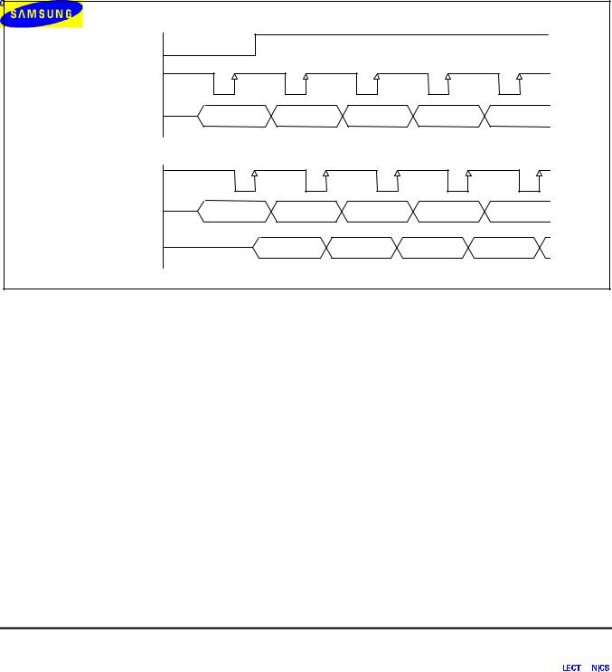
65 COM / 132 SEG DRIVER & CONTROLLER FOR STN LCD |
S6B1713 |
|
|
Data Transfer
The S6B1713 uses bus holder and internal data bus for Data Transfer with the MPU. When writing data from the MPU to on-chip RAM, data is automatically transferred from the bus holder to the RAM as shown in figure 4. And when reading data from on-chip RAM to the MPU, the data for the initial read cycle is stored in the bus holder (dummy read) and the MPU reads this stored data from bus holder for the next data read cycle as shown in figure 5. This means that a dummy read cycle must be inserted between each pair of address sets when a sequence of address sets is executed. Therefore, the data of the specified address cannot be output with the read display data instruction right after the address sets, but can be output at the second read of data.
MPU signals
RS |
|
|
|
|
|
/WR |
|
|
|
|
|
DB0 to DB7 |
N |
D(N) |
D(N+1) |
D(N+2) |
D(N+3) |
Internal signals
/WR |
|
|
|
|
|
BUS HOLDER |
N |
D(N) |
D(N+1) |
D(N+2) |
D(N+3) |
COLUMN ADDRESS |
N |
|
N+1 |
N+2 |
N+3 |
Figure 4. Write Timing
16
S6B1713 |
65 COM / 132 SEG DRIVER & CONTROLLER FOR STN LCD |
|
|
MPU signals
RS |
|
/WR |
|
/RD |
|
DB0 to DB7 |
N |
Internal signals
/WR |
|
|
|
|
|
|
|
|
|
/RD |
|
|
|
|
|
|
|
|
|
BUS HOLDER |
|
|
N |
|
|
|
|||
COLUMN ADDRESS |
|
|
|
N |
|
|
|
||
|
|
|
|
|
Dummy |
D(N) |
D(N+1) |
D(N) |
D(N+1) |
D(N+2) |
N+1 |
N+2 |
N+3 |
Figure 5. Read Timing
17
 Loading...