


S3C8465/C8469/P8469 |
PRODUCT OVERVIEW |
|
|
1 PRODUCT OVERVIEW
SAM8 PRODUCT FAMILY
Samsung's new SAM8 family of 8-bit single-chip CMOS microcontrollers offers a fast and efficient CPU, a wide range of integrated peripherals, and various mask-programmable ROM sizes.
A dual address/data bus architecture and a large number of bitor nibble-configurable I/O ports provide a flexible programming environment for applications with varied memory and I/O requirements. Timer/counters with selectable operating modes are included to support real-time operations. Many SAM8 microcontrollers have an external interface that provides access to external memory and other peripheral devices.
A sophisticated interrupt structure recognizes up to eight interrupt levels. Each level can have one or more interrupt sources and vectors. Fast interrupt processing (within a minimum six CPU clocks) can be assigned to one interrupt level at a time.
S3C8465/C8469 MICROCONTROLLER
The S3C8465/C8469 single-chip 8-bit microcontroller is designed for useful 10-bit resolution A/D converter, UART, SIO, ZCD extended PWM application field. Its powerful SAM87 CPU architecture includes. The internal register file is logically expanded to increase the on-chip register space.
The S3C8465/C8469 has 16/32K bytes of on-chip program ROM. A sophisticated bus interface enables access to external memory and other peripherals when you use the chip in ROM-less mode. Following Samsung's modular design approach, the following peripherals are integrated with the SAM87 core:
—Large number of programmable I/O ports (total 56 pins)
—One asynchronous UART module
—One synchronous SIO module
—Analog-to-digital converter with eight input channels and 10-bit resolution
—One 8-bit basic timer for watchdog function
—One 8-bit timer/counter with three operating modes (timer 0)
—One 8-bit timer for zero-cross detection circuit (timer 2)
—Two general-purpose 16-bit timer/counters with four operating modes (timer module 1)
—PWM block with one capture module, 16-bit timer/counter, PWM extension mode, and two PWM outputs
—One zero cross detection module
The S3C8465/C8469 is a versatile general-purpose microcontroller that is ideal for use in a wide range of electronics applications requiring complex timer/counter, PWM, capture, SIO, UART and ZCD functions. It is available in a 64-pin SDIP or 64-pin QFP package.
OTP
The S3P8469 is an OTP (One Time Programmable) version of the S3C8465/C8469 microcontroller. The S3P8469 microcontroller has an on-chip 32-Kbyte one-time-programmable EPROM instead of a masked ROM. The S3P8469 is comparable to the S3C8465/C8469, both in function and in pin configuration.
1-1

PRODUCT OVERVIEW |
S3C8465/C8469/P8469 |
|
|
FEATURES
CPU
•SAM87 CPU core
Memory
•528-byte general purpose register area
•16/32K-byte internal program memory
•ROM-less operating mode
External Interface
•64K-byte external data memory area
•64K-byte external program memory area (ROM-less mode)
Instruction Set
•79 instructions
•IDLE and STOP instructions added for power-down modes
Instruction Execution Time
•500 ns at 12 MHz fOSC (minimum)
Interrupts
•21 interrupt sources and 21 vectors
•Eight interrupt levels
•Fast interrupt processing
General I/O
•Seven I/O ports (total 56 pins)
•Seven bit-programmable ports
PWM and Capture
•Two 14-bit PWM output
•One capture
Serial I/O
•One synchronous serial I/O module
•Selectable transmit and receive rates
•Selectable baud rate for Rx and Tx respectively
Timer/Counters
•One 8-bit basic timer for watchdog function
•One 8-bit timer/counter with three operating modes (timer 0)
•One 8-bit timer for the zero-cross detection circuit
•Two 16-bit general-purpose timer/counters with four operating modes (timer C and D)
UART
•One UART module
•Full duplex serial I/O interface with three UART modes
A/D Converter
•Eight analog input pins
•10-bit conversion resolution
•20 µs conversion time (10 MHz CPU clock)
Zero Cross Detection Circuit
•Zero cross detection circuit that generates a digital signal in synchronization with an AC signal input
Buzzer Frequency Output
•200 Hz to 20 kHz signal can be generated
Oscillator Frequency
•1 MHz to 12 MHz external crystal oscillator
•Maximum 12 MHz CPU clock
Operating Temperature Range
•– 40°C to + 85°C
Operating Voltage Range
•2.7 V to 5.5 V
Package Types
•64-pin SDIP, 64-pin QFP
1-2
S3C8465/C8469/P8469 |
PRODUCT OVERVIEW |
|
|
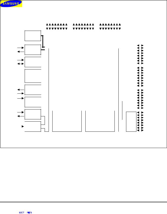
BLOCK DIAGRAM
Basic
Timer
XIN
OSC
XOUT
T0CK
Timer
T0
TCG 
TDG  Timers TCCK
  C and D TDCK
PWM0  PWM/ PWM1 CAP CAPA
SI
SO  SIO
SIO
SCK 

RxD
UART
TxD
ADC0 
 ADC -ADC7
|
|
|
|
P0.0-P0.7 |
|
|
|
|
|
|
P1.0-P1.7 |
|
|
P2.0-P2.3 |
|
|
|
|||||||||||||||||||||
|
|
|
|
(A8-A15) |
|
|
|
|
|
(AD0-AD7) P2.4/ZCD-P2.7/INT3 |
|
|
|
|||||||||||||||||||||||||
|
|
|
|
|
|
|
|
|
|
|
|
|
|
|
|
|
|
|
|
|
|
|
|
|
|
|
|
|
|
|
|
|
|
|
|
|
||
|
|
|
|
|
|
|
|
|
|
|
|
|
|
|
|
|
|
|
|
|
|
|
|
|
|
|
|
|
|
|
|
|
|
|
|
|
|
|
|
|
|
|
|
|
|
|
|
|
|
|
|
|
|
|
|
|
|
|
|
|
|
|
|
|
|
|
|
|
|
|
|
|
|
|
|
|
|
|
|
|
|
|
Port 0 |
|
|
|
|
|
|
|
Port 1 |
|
|
|
|
|
Port 0 |
|
|
|
|
|
||||||||||||||
|
|
|
|
|
|
|
|
|
|
|
|
|
|
|
|
|
|
|
|
|
|
|
|
|
|
|
|
|
|
|
|
|
|
|
|
|
|
|
|
|
|
|
|
|
|
|
|
|
|
|
|
|
|
|
|
|
|
|
|
|
|
|
|
|
|
|
|
|
|
|
|
|
|
|
|
|
|
|
|
|
|
|
|
|
|
|
|
|
|
|
|
SAM8 BUS |
|
|
|
|
|
|
|
|
|
|
|
Port 3 |
|
|
P3.0-P3.7 |
|||||||||
|
|
|
|
|
|
|
|
|
|
|
|
|
|
|
|
|
|
|
|
|
|
|
|
|
|
|
|
|
|
|
|
|
|
|
|
|
||
|
|
|
|
|
|
|
|
|
|
|
|
|
|
|
|
|
|
|
|
|
|
|
|
|
|
|
|
|
|
|
|
|
|
|
|
|
||
|
|
|
|
|
|
|
|
|
|
|
|
|
|
|
|
|
|
|
|
|
|
|
|
|
|
|
|
|
|
|
|
|
|
|
|
|
||
|
|
|
|
|
|
|
|
|
|
|
Port I/O and Interrupt |
|
|
|
|
|
|
|
|
|
|
|
|
|
||||||||||||||
|
|
|
|
|
|
|
|
|
|
|
|
|
|
|
|
|
|
|
|
|
|
|
|
|||||||||||||||
|
|
|
|
|
|
|
|
|
|
|
|
|
|
|
|
|
|
|
|
|
|
|
|
|
|
|||||||||||||
|
|
|
|
|
|
|
|
|
|
|
|
|
|
|
|
|
|
|
|
|
|
|
|
|
|
|||||||||||||
|
|
|
|
|
|
|
|
|
|
|
|
|
|
|
|
|
|
|
|
|
|
|
|
|
|
|||||||||||||
|
|
|
|
|
|
|
|
|
|
|
|
|
|
|
|
|
|
|
|
|
|
|
|
|
|
|||||||||||||
|
|
|
|
|
|
|
|
|
|
|
|
|
|
|
Control |
|
|
|
|
|
|
|
|
|
|
|
|
|
|
P4.0/INT4- |
||||||||
|
|
|
|
|
|
|
|
|
|
|
|
|
|
|
|
|
|
|
|
|
|
|
|
|
|
|
|
|
||||||||||
|
|
|
|
|
|
|
|
|
|
|
|
|
|
|
|
|
|
|
|
|
|
|
|
|
|
|
|
|
||||||||||
|
|
|
|
|
|
|
|
|
|
|
|
|
|
|
|
|
|
|
|
|
|
|
|
|
|
|
|
|
|
|
|
|
|
|
|
|
|
|
|
|
|
|
|
|
|
|
|
|
|
|
|
|
|
|
|
|
|
|
|
|
|
|
|
|
|
|
|
|
|
|
|
|
|
Port 4 |
|
|
|
|
|
|
|
|
|
|
|
|
|
|
|
|
|
|
|
|
|
|
|
|
|
|
|
|
|
|
|
|
|
|
|
|
|
|
|
|
||
|
|
|
|
|
|
|
|
|
|
|
|
|
|
|
|
|
|
|
|
|
|
|
|
|
|
|
|
|
|
|
|
|
|
|
|
|
||
|
|
|
|
|
|
|
|
|
|
|
|
|
|
SAM8 CPU |
|
|
|
|
|
|
|
|
|
|
|
|
|
P4.7/INT11 |
||||||||||
|
|
|
|
|
|
|
|
|
|
|
|
|
|
|
|
|
|
|
|
|
|
|
|
|
|
|
|
|||||||||||
|
|
|
|
|
|
|
|
|
|
|
|
|
|
|
|
|
|
|
|
|
|
|
|
|
|
|
|
|
||||||||||
|
|
|
|
|
|
|
|
|
|
|
|
|
|
|
|
|
|
|
|
|
|
|
|
|
|
|
|
|
||||||||||
|
|
|
|
|
|
|
|
|
|
|
|
|
|
|
|
|
|
|
|
|
|
|
|
|
|
|
|
|
||||||||||
|
|
|
|
|
|
|
|
|
|
|
|
|
|
|
|
|
|
|
|
|
|
|
|
|
|
|
|
|
||||||||||
|
|
|
|
|
|
|
|
|
|
|
|
|
|
|
|
|
|
|
|
|
|
|
|
|
Port 5 |
|
|
P5.0-P5.7 |
||||||||||
|
|
|
|
|
|
|
|
|
|
|
|
|
|
|
|
|
|
|
|
|
|
|
|
|
|
|
|
|
|
|
|
|
|
|
|
|
||
|
|
|
|
|
|
|
|
|
|
|
|
|
|
|
|
|
|
|
|
|
|
|
|
|
|
|
|
|
|
|
|
|
|
|
|
|
||
|
|
|
|
|
|
|
|
|
|
|
|
|
|
|
|
|
|
|
|
|
|
|
|
|
|
|
|
|
|
|
|
|
|
|
|
|
||
|
|
|
|
|
|
|
|
|
|
|
|
|
|
|
|
|
|
|
|
|
|
|
|
|
|
|
|
|
|
|
|
|
|
|
|
|
||
|
|
|
|
|
|
|
|
|
|
|
|
|
|
|
|
|
|
|
|
|
|
|
|
|
|
|
|
|
|
|
|
|
|
|
|
|
|
|
|
|
|
|
|
|
|
|
|
|
|
|
|
|
|
|
|
|
|
|
|
|
|
|
|
|
|
|
|
|
|
|
|
|
|
|
|
|
|
|
|
|
|
|
|
|
|
|
|
|
|
|
|
|
|
|
|
|
|
|
|
|
|
|
|
|
|
|
|
|
|
|
|
|
|
|
|
|
|
|
|
|
|
|
|
|
|
|
|
|
|
|
|
|
|
|
|
|
|
|
|
|
|
|
|
|
|
|
|
|
|
|
|
|
|
|
|
|
|
|
|
|
|
|
|
|
|
|
|
|
|
|
|
|
|
|
|
|
|
|
|
|
|
|
|
|
|
|
|
|
|
|
|
|
|
|
|
|
|
|
|
|
|
|
|
|
|
|
|
|
|
|
|
|
|
|
|
|
|
|
|
|
|
|
|
|
|
|
|
|
|
|
|
|
|
|
|
|
|
|
|
|
|
|
|
|
|
|
|
|
|
|
|
|
|
|
|
|
|
|
|
|
|
|
|
|
|
|
|
|
|
|
|
|
16/32-Kbyte |
528-byte |
|
Port 6 |
|
P6.0-P6.7 |
|
|
|
|||||
ROM |
Register File |
|
|
|||
|
|
|
|
|||
|
|
|
|
|
|
|
|
|
|
|
|
|
|
|
|
|
|
|
|
|
Figure 1-1. Block Diagram
1-3
PRODUCT OVERVIEW |
S3C8465/C8469/P8469 |
|
|
PIN ASSIGNMENTS
|
|
|
|
|
|
|
|
P1.0/AD0 |
P0.7/A15 |
|
1 |
|
|
|
64 |
|
|
|
|
|
|
|
||||
P0.6/A14 |
|
2 |
|
|
|
63 |
|
P1.1/AD1 |
|
|
|
|
|
||||
P0.5/A13 |
|
3 |
|
|
|
62 |
|
P1.2/AD2 |
|
|
|
|
|
||||
P0.4/A12 |
|
4 |
|
|
|
61 |
|
P1.3/AD3 |
|
|
|
|
|
||||
P0.3/A11 |
|
5 |
|
|
|
60 |
|
P1.4/AD4 |
|
|
|
|
|
||||
P0.2/A10 |
|
6 |
|
|
|
59 |
|
P1.5/AD5 |
|
|
|
|
|
||||
P0.1/A9 |
|
7 |
|
|
|
58 |
|
P1.6/AD6 |
|
|
|
|
|
||||
P0.0/A8 |
|
8 |
|
|
|
57 |
|
P1.7/AD7 |
|
|
|
|
|
||||
P4.7/INT11/TDG |
|
9 |
|
|
|
56 |
|
P5.7/ADC7 |
|
|
|
|
|
||||
P4.6/INT10/TCG |
|
10 |
|
|
|
55 |
|
P5.6/ADC6 |
|
|
|
|
|
||||
P4.5/INT9/TDCK |
|
11 |
|
|
|
54 |
|
P5.5/ADC5 |
|
|
|
|
|
||||
P4.4/INT8/TCCK |
|
12 |
|
|
|
53 |
|
P5.4/ADC4 |
|
|
|
|
|
||||
P4.3/INT7/CAPA |
|
13 |
S3C8465 |
52 |
|
P5.3/ADC3 |
||
|
|
|||||||
P4.2/INT6 |
|
14 |
51 |
|
P5.2/ADC2 |
|||
|
|
|||||||
P4.1/INT5/RxD |
|
15 |
S3C8469 |
50 |
|
P5.1/ADC1 |
||
|
|
|||||||
VDD |
|
16 |
49 |
|
P5.0/ADC0 |
|||
|
|
|||||||
VSS |
|
17 |
64-SDIP-750 |
48 |
|
AVSS |
||
|
|
|||||||
XOUT |
|
18 |
|
|
|
47 |
|
AVREF |
|
|
|
|
|
||||
XIN |
|
19 |
(Top View) |
46 |
|
P6.7 |
||
|
|
|||||||
EA |
|
20 |
|
|
|
45 |
|
P6.6 |
|
|
|
|
|
||||
P4.0/INT4 |
|
21 |
|
|
|
44 |
|
P6.5 |
|
|
|
|
|
||||
P3.7/TxD |
|
22 |
|
|
|
43 |
|
P6.4 |
|
|
|
|
|
||||
|
|
|
|
|
||||
RESET |
|
23 |
|
|
|
42 |
|
P6.3 |
|
|
|
|
|
||||
|
|
|
|
|
||||
P3.6/SO |
|
24 |
|
|
|
41 |
|
P6.2 |
|
|
|
|
|
||||
|
|
|
|
|
||||
P3.5/SI |
|
25 |
|
|
|
40 |
|
P6.1 |
|
|
|
|
|
||||
|
|
|
|
|
||||
P3.4/SCK |
|
26 |
|
|
|
39 |
|
P6.0 |
|
|
|
|
|
||||
|
|
|
|
|
||||
P3.3/T0CK |
|
27 |
|
|
|
38 |
|
P2.0/AS |
|
|
|
|
|
||||
|
|
|
|
|
||||
P3.2/T0 |
|
28 |
|
|
|
37 |
|
P2.1/DS |
|
|
|
|
|
||||
|
|
|
|
|
||||
P3.1/PWM1 |
|
29 |
|
|
|
36 |
|
P2.2/R/W |
|
|
|
|
|
||||
|
|
|
|
|
||||
P3.0/PWM0 |
|
30 |
|
|
|
35 |
|
P2.3/DM |
|
|
|
|
|
||||
|
|
|
|
|
||||
P2.7/INT3 |
|
31 |
|
|
|
34 |
|
P2.4/ZCD |
|
|
|
|
|
||||
|
|
|
|
|
||||
P2.6/INT2 |
|
32 |
|
|
|
33 |
|
P2.5/BUZ |
|
|
|
|
|
||||
|
|
|
|
|
||||
|
|
|
|
|
|
|
|
|
Figure 1-2. Pin Assignment Diagram (64-SDIP)
1-4
S3C8465/C8469/P8469 |
PRODUCT OVERVIEW |
|
|
|
|
P0.1/A9 |
P0.2/A10 |
P0.3/A11 |
P0.4/A12 |
P0.5/A13 |
P0.6/A14 |
P0.7/A15 |
P1.0/AD0 |
P1.1/AD1 |
P1.2/AD2 |
P1.3/AD3 |
P1.4/AD4 |
P1.5/AD5 |
|
|
||||||||||||||||||||||||||
|
|
|
|
|
|
|
|
|
|
|
|
|
|
|
|
|
||||||||||||||||||||||||||
|
|
|
|
|
|
|
|
|
|
|
|
|
|
|
|
|
|
|
|
|
|
|
|
|
|
|
|
|
|
|
|
|
|
|
|
|
|
|
|
|
|
|
|
|
64 |
63 |
62 |
61 |
60 |
59 |
58 |
57 |
56 |
55 |
54 |
53 |
52 |
|
|
||||||||||||||||||||||||||
P0.0/A8 |
|
1 |
|
|
|
|
|
|
|
|
|
|
|
|
|
|
|
|
|
|
|
|
|
|
|
|
|
|
|
|
|
|
|
|
|
|
|
51 |
|
|
||
|
|
|
|
|
|
|
|
|
|
|
|
|
|
|
|
|
|
|
|
|
|
|
|
|
|
|
|
|
|
|
|
|
|
|
|
|
|
|||||
P4.7/INT11/TDG |
|
2 |
|
|
|
|
|
|
|
|
|
|
|
|
|
|
|
|
|
|
|
|
|
|
|
|
|
|
|
|
|
|
|
|
|
|
|
50 |
|
|
||
|
|
|
|
|
|
|
|
|
|
|
|
|
|
|
|
|
|
|
|
|
|
|
|
|
|
|
|
|
|
|
|
|
|
|
|
|
|
|||||
P4.6/INT10/TCG |
|
3 |
|
|
|
|
|
|
|
|
|
|
|
|
|
|
|
|
|
|
|
|
|
|
|
|
|
|
|
|
|
|
|
|
|
|
|
49 |
|
|
||
|
|
|
|
|
|
|
|
|
|
|
|
|
|
|
|
|
|
|
|
|
|
|
|
|
|
|
|
|
|
|
|
|
|
|
|
|
|
|||||
P4.5/INT9/TDCK |
|
4 |
|
|
|
|
|
|
|
|
|
|
|
|
|
|
|
|
|
|
|
|
|
|
|
|
|
|
|
|
|
|
|
|
|
|
|
48 |
|
|
||
|
|
|
|
|
|
|
|
|
|
|
|
|
|
|
|
|
|
|
|
|
|
|
|
|
|
|
|
|
|
|
|
|
|
|
|
|
|
|||||
P4.4/INT8/TCCK |
|
5 |
|
|
|
|
|
|
|
|
|
|
|
|
|
|
|
|
|
|
|
|
|
|
|
|
|
|
|
|
|
|
|
|
|
|
|
47 |
|
|
||
|
|
|
|
|
|
|
|
|
|
|
|
|
|
|
|
|
|
|
|
|
|
|
|
|
|
|
|
|
|
|
|
|
|
|
|
|
|
|||||
P4.3/INT7CAPA |
|
6 |
|
|
|
|
|
|
|
|
|
|
|
|
|
|
|
|
|
|
|
|
|
|
|
|
|
|
|
|
|
|
|
|
|
|
|
46 |
|
|
||
|
|
|
|
|
|
|
|
|
|
|
|
|
|
|
|
|
|
|
|
|
|
|
|
|
|
|
|
|
|
|
|
|
|
|
|
|
|
|||||
P4.2/INT6 |
|
7 |
|
|
|
|
|
|
|
|
|
|
|
|
|
|
|
|
|
|
|
|
|
|
|
|
|
|
|
|
|
|
|
|
|
|
|
45 |
|
|
||
|
|
|
|
|
|
|
|
|
|
|
|
|
|
|
|
|
|
|
|
|
|
|
|
|
|
|
|
|
|
|
|
|
|
|
|
|
|
|||||
P4.1/INT5/RxD |
|
8 |
|
|
|
|
S3C8465/C8469 |
44 |
|
|
||||||||||||||||||||||||||||||||
|
|
|
|
|
|
|
||||||||||||||||||||||||||||||||||||
VDD |
|
9 |
|
|
|
|
|
|
|
|
|
64-QFP-1420F |
|
|
|
|
|
|
43 |
|
|
|||||||||||||||||||||
VSS |
|
10 |
|
|
|
|
|
|
|
|
|
|
|
|
|
|
|
|
|
|
|
|
|
|
|
|
|
|
|
|
|
|
|
|
|
|
|
42 |
|
|
||
XOUT |
|
11 |
|
|
|
|
|
|
|
|
|
|
|
(Top View) |
|
|
|
|
|
|
|
|
|
41 |
|
|
||||||||||||||||
|
|
|
|
|
|
|
|
|
|
|
|
|
|
|
|
|
|
|
|
|
|
|
||||||||||||||||||||
XIN |
|
12 |
|
|
|
|
|
|
|
|
|
|
|
|
|
|
|
|
|
|
|
|
40 |
|
|
|||||||||||||||||
EA |
|
13 |
|
|
|
|
|
|
|
|
|
|
|
|
|
|
|
|
|
|
|
|
|
|
|
|
|
|
|
|
|
|
|
|
|
|
|
39 |
|
|
||
|
|
|
|
|
|
|
|
|
|
|
|
|
|
|
|
|
|
|
|
|
|
|
|
|
|
|
|
|
|
|
|
|
|
|
|
|
|
|||||
P4.0/INT4 |
|
14 |
|
|
|
|
|
|
|
|
|
|
|
|
|
|
|
|
|
|
|
|
|
|
|
|
|
|
|
|
|
|
|
|
|
|
|
38 |
|
|
||
|
|
|
|
|
|
|
|
|
|
|
|
|
|
|
|
|
|
|
|
|
|
|
|
|
|
|
|
|
|
|
|
|
|
|
|
|
|
|||||
P3.7/TxD |
|
15 |
|
|
|
|
|
|
|
|
|
|
|
|
|
|
|
|
|
|
|
|
|
|
|
|
|
|
|
|
|
|
|
|
|
|
|
37 |
|
|
||
|
|
|
|
|
|
|
|
|
|
|
|
|
|
|
|
|
|
|
|
|
|
|
|
|
|
|
|
|
|
|
|
|
|
|
|
|
|
|||||
RESET |
|
16 |
|
|
|
|
|
|
|
|
|
|
|
|
|
|
|
|
|
|
|
|
|
|
|
|
|
|
|
|
|
|
|
|
|
|
|
36 |
|
|
||
|
|
|
|
|
|
|
|
|
|
|
|
|
|
|
|
|
|
|
|
|
|
|
|
|
|
|
|
|
|
|
|
|
|
|
|
|
|
|||||
P3.6/SO |
|
17 |
|
|
|
|
|
|
|
|
|
|
|
|
|
|
|
|
|
|
|
|
|
|
|
|
|
|
|
|
|
|
|
|
|
|
|
35 |
|
|
||
P3.5/SI |
|
18 |
|
|
|
|
|
|
|
|
|
|
|
|
|
|
|
|
|
|
|
|
|
|
|
|
|
|
|
|
|
|
|
|
|
|
|
34 |
|
|
||
P3.4/SCK |
|
19 |
|
|
|
|
|
|
|
|
|
|
|
|
|
|
|
|
|
|
|
|
|
|
|
|
|
|
|
|
|
|
|
|
|
|
|
33 |
|
|
||
|
|
|
|
|
|
|
|
|
|
|
|
|
|
|
|
|
|
|
|
|
|
|
|
|
|
|
|
|
|
|
|
|
|
|
|
|
|
|||||
|
|
20 |
21 |
22 |
23 |
24 |
25 |
26 |
27 |
28 |
29 |
30 |
31 |
32 |
|
|
||||||||||||||||||||||||||
|
|
|
|
|
|
|
|
|
|
|
|
|
|
|
|
|
|
|
|
|
|
|
|
|
|
|
|
|
|
|
|
|
|
|
|
|
|
|
|
|
|
|
|
|
|
|
|
|
|
|
|
|
|
|
|
|
|
|
|
|
|
|
|
|
|
|
|
|
|
|
|
|
|
|
|
|
|
|
|
|
|
|
|
|
|
|
|
P3.3/T0CK |
P3.2/T0 |
P3.1/PWM1 |
P3.0/PWM0 |
P2.7/INT3 |
P2.6/INT2 |
P2.5/BUZ |
P2.4/ZCD |
P2.3/DM |
P2.2/R/W |
P2.1/DS |
P2.0/AS |
P6.0 |
|
|
||||||||||||||||||||||||||
P1.6/AD6
P1.7/AD7
P5.7/ADC7
P5.6/ADC6
P5.5/ADC5
P5.4/ADC4
P5.3/ADC3
P5.2/ADC2
P5.1/ADC1
P5.0/ADC0 AVSS
AVREF
P6.7
P6.6
P6.5
P6.4
P6.3
P6.2
P6.1
Figure 1-3. Pin Assignment Diagram (64-Pin QFP Package)
1-5

PRODUCT OVERVIEW |
S3C8465/C8469/P8469 |
|
|
Table 1-1. S3C8465/C8469 Pin Descriptions
Pin |
Pin |
Pin Description |
Circuit |
Pin |
Share |
Name |
Type |
|
Number |
Number |
Pins |
|
|
|
|
|
|
P0.0–P0.7 |
I/O |
Bit-programmable I/O port for Schmitt trigger |
1 |
8–1 |
– |
|
|
input or push-pull, open-drain, output. Pull-up |
|
(1, 64–58) |
A8–A15 |
|
|
resistors are assignable by software. |
|
|
|
|
|
Port 0 can also be configured as external |
|
|
|
|
|
interface address line A8–A15 |
|
|
|
|
|
|
|
|
|
P1.0–P1.7 |
I/O |
Same general characteristics as port 0. |
1 |
64–57 |
– |
|
|
Port 1 can also be configured as external |
|
(57–50) |
AD0–AD7 |
|
|
interface address/data lines AD0–AD7 |
|
|
|
|
|
|
|
|
|
P2.0–P2.3 |
I/O |
Bit-programmable I/O port for Schmitt trigger |
2 |
38–35 |
– |
|
|
input or push-pull output. P2.0–P2.3 can be |
|
(31–28) |
AS, DS |
|
|
configured for external bus control signals. |
|
|
DM, R/W |
P2.4–P2.7 |
|
P2.4–P2.7 are used for general I/O or for the |
3 |
34–31 |
ZCD, BUZ |
|
ZCD, BUZ, INT2 and INT3 |
INT2, INT3 |
|||
|
|
|
(27–24) |
||
|
|
|
|
|
|
|
|
|
|
|
|
P3.0–P3.7 |
I/O |
Bit-programmable I/O port for Schmitt trigger |
4 |
30–22 |
(See pin |
|
|
input or push-pull output. Each port 3 pin has |
|
(23–15) |
description) |
|
|
an alternative function: |
|
|
|
|
|
P3.0: PWM0 (PWM0 module output) |
|
|
|
|
|
P3.1: PWM1 (PWM1 module ouptut) |
|
|
|
|
|
P3.2: T0 (T0 capture input or PWM output) |
|
|
|
|
|
P3.3: T0CK (timer 0 external clock input) |
|
|
|
|
|
P3.4: SCK (SIO module input) |
|
|
|
|
|
P3.5: SI (SIO module clock I/O) |
|
|
|
|
|
P3.6: SO (SIO module output) |
|
|
|
|
|
P3.7: TxD: SO1 |
|
|
|
|
|
(The T0 function for P3.2 is selected using the |
|
|
|
|
|
T0CON register.) |
|
|
|
|
|
|
|
|
|
P4.0–P4.7 |
I/O |
Bit-programmable I/O port for Schmitt trigger |
5 |
21, 15–9 |
(See pin |
|
|
input or push-pull output. Port 4 pins are used |
|
(14–2) |
description) |
|
|
external interrupts INT4–INT11 or for the |
|
|
|
|
|
following share functions: |
|
|
|
|
|
P4.1: RxD (UART module input) |
|
|
|
|
|
P4.3: CAPA (capture input) |
|
|
|
|
|
P4.4: TCCK (timer/counter C clock input) |
|
|
|
|
|
P4.5: TDCK (timer/counter D clock input) |
|
|
|
|
|
P4.6: TCG (timer C gate input) |
|
|
|
|
|
P4.7: TDG (timer D gate input) |
|
|
|
|
|
|
|
|
|
1-6

S3C8465/C8469/P8469 |
PRODUCT OVERVIEW |
|
|
Table 1-1. S3C8465/C8469 Pin Descriptions (Continued)
Pin |
Pin |
Pin Description |
Circuit |
Pin |
Share |
|
Name |
Type |
|
Number |
Number |
Pins |
|
|
|
|
|
|
|
|
P5.0–P5.7 |
I/O |
Bit-programmable I/O port for Schmitt trigger |
6 |
49–56 |
ADC0– |
|
|
|
input or push-pull, output. Pull-up resistors are |
|
(42–49) |
ADC7 |
|
|
|
assignable by software. Port 5 pins can also be |
|
|
|
|
|
|
used as A/D converter inputs. |
|
|
|
|
|
|
|
|
|
|
|
P6.0–P6.7 |
I/O |
Individual pins are software configurable as |
1 |
39–46 |
– |
|
|
|
input or push-pull, open-drain, output. Pull-up |
|
(32–39) |
|
|
|
|
resistors are assignable by software. |
|
|
|
|
|
|
|
|
|
|
|
AD0–AD7 |
I/O |
External interface address/data line |
6 |
64–57 |
P1.0–P1.7 |
|
|
|
|
|
(57–50) |
|
|
|
|
|
|
|
|
|
AS |
I/O |
External bus control signals |
2 |
38–35 |
P2.0–P2.3 |
|
DS |
|
|
|
(31–28) |
|
|
R/W |
|
|
|
|
|
|
DM |
|
|
|
|
|
|
|
|
|
|
|
|
|
ZCD |
I/O |
Zero cross detector input |
2 |
34 (27) |
P2.4 |
|
|
|
|
|
|
|
|
BUZ |
I/O |
200 Hz–20 kHz frequency output for buzzer |
2 |
33 (26) |
P2.5 |
|
|
|
sound |
|
|
|
|
|
|
|
|
|
|
|
PWM0 |
I/O |
PWM output |
3 |
30, |
29 |
P3.0–P3.1 |
PWM1 |
|
|
|
(23, |
22) |
|
|
|
|
|
|
|
|
T0 (CAP) |
I/O |
T0 capture input or PWM output |
3 |
28 (21) |
P3.2 |
|
|
|
|
|
|
|
|
T0CK |
I/O |
External clock input for Timer 0 |
3 |
27 (20) |
P3.3 |
|
|
|
|
|
|
|
|
SCK |
I/O |
SIO clock signal |
3 |
26 (19) |
P3.4 |
|
|
|
|
|
|
|
|
SI, SO |
I/O |
SIO data input/output |
3 |
25, |
24 |
P3.5–P3.6 |
|
|
|
|
(18, |
17) |
|
|
|
|
|
|
|
|
TxD |
I/O |
UART data output |
3 |
22 (15) |
P3.7 |
|
|
|
|
|
|
|
|
INT2–INT3 |
I/O |
External interrupts: the triggering edge is |
2 |
32, |
31 |
P2.6–P2.7 |
|
|
selectable. |
|
(25, |
24) |
|
|
|
|
|
|
|
|
INT4 |
I/O |
External interrupts: the triggering edge is |
4 |
21 (14) |
P4.0 |
|
|
|
selectable. |
|
|
|
|
|
|
|
|
|
|
|
RxD/INT5 |
I/O |
UART data input or external interrupt: the |
4 |
15 (8) |
P4.1 |
|
|
|
triggering edge is selectable. |
|
|
|
|
|
|
|
|
|
|
|
INT6 |
I/O |
Capture module input or external interrupt: the |
4 |
14,13 |
P4.2–P4.3 |
|
CAPA/INT7 |
|
triggering edge is selectable. |
|
(7, |
6) |
|
|
|
|
|
|
|
|
1-7

PRODUCT OVERVIEW |
S3C8465/C8469/P8469 |
|
|
Table 1-1. S3C8465/C8469 Pin Descriptions (Concluded)
Pin |
Pin |
Pin Description |
Circuit |
Pin |
Share |
|
Name |
Type |
|
Number |
Number |
Pins |
|
|
|
|
|
|
|
|
TCCK/INT8 |
I/O |
Timer/counter C and D clock input or external |
4 |
12, |
11 |
P4.4–P4.5 |
TCDK/INT9 |
|
interrupts: the triggering edge is selectable. |
|
(5, |
4) |
|
|
|
|
|
|
|
|
TCG/INT10 |
I/O |
Timer/counter C and D clock input or external |
4 |
10, 9 |
P4.6–P4.7 |
|
TDG/INT11 |
|
interrupts: the triggering edge is selectable. |
|
(3, |
2) |
|
|
|
|
|
|
|
|
ADC0– |
I/O |
A/D converter inputs |
5 |
49–56 |
P5.0–P5.7 |
|
ADC7 |
|
|
|
(42–49) |
|
|
|
|
|
|
|
|
|
XIN, XOUT |
– |
System clock input and output pins |
– |
19, |
18 |
– |
|
|
|
|
(12, |
11) |
|
RESET |
I |
System reset pin |
7 |
23 (16) |
– |
|
|
|
|
|
|
|
|
EA |
I |
External access (EA) pin with three modes: |
– |
20 (13) |
– |
|
|
|
0 V: Normal operation (internal ROM) |
|
|
|
|
|
|
5 V: ROM-less operation (external interface) |
|
|
|
|
|
|
12.5 V: OTP read/write mode |
|
|
|
|
|
|
|
|
|
|
|
AVREF, |
– |
A/D converter reference voltage input and |
– |
47, |
48 |
– |
AVSS |
|
ground |
|
(40, |
41) |
|
VDD ,VSS |
– |
Voltage input pin and ground |
– |
16, |
17 |
– |
|
|
|
|
(9, 10) |
|
|
NOTE: Pin numbers shown in parentheses "( )" are for the 64-pin QFP package.
1-8

S3C8465/C8469/P8469 PRODUCT OVERVIEW
PIN CIRCUITS
Table 1-2. Pin Circuit Assignments for the S3C8465/C8469
Circuit Number |
Circuit Type |
S3C8465/C8469 Assignments |
|
|
|
1 |
I/O |
Port 0,1 and port 6 |
|
|
|
2 |
I/O |
Port 2 (P2.0–P2.3 only) |
|
|
|
3 |
I/O |
Port 2 (P2.4–P2.7 only) |
|
|
|
4 |
I/O |
Port 3 |
|
|
|
5 |
I/O |
Port 4 |
|
|
|
6 |
I/O |
Port 5 |
|
|
|
7 |
I |
RESET |
|
|
|
NOTE: Diagrams of circuit types 1–7 are presented below.
1-9

PRODUCT OVERVIEW |
S3C8465/C8469/P8469 |
|
|
VDD
Pull-up |
Enable |
VDD |
Data |
Open-drain |
Output DIsable |
In |
Pull-up Resistor
(Typical Value: 47 KΩ)
In/Out
Figure 1-4. Pin Circuit Type 1 (Port 0,1 and Port 6)
VDD
Pull-up
Enable
Port 2 (Low Byte) Data
External Interface
(AS, DS, R/W, DM)
Output DIsable
In
Select |
VDD |
|
|
M |
Data |
U |
|
X |
|
Pull-up Resistor
(Typical Value: 47 KΩ)
In/Out
Figure 1-5. Pin Circuit Type 2 (Port 2, P2.0–P2.3 only)
1-10
 Loading...