


S3C9404/P9404/C9414/P9414 |
PRODUCT OVERVIEW |
|
|
1 PRODUCT OVERVIEW
SAM87RI PRODUCT FAMILY
Samsung's SAM87Ri family of 8-bit single-chip CMOS microcontrollers offers a fast and efficient CPU, a wide range of integrated peripherals, and various mask-programmable ROM sizes.
A address/data bus architecture and a large number of bit-configurable I/O ports provide a flexible programming environment for applications with varied memory and I/O requirements. Timer/counters with selectable operating modes are included to support real-time operations.
S3C9404/C9414 MICROCONTROLLER
The S3C9404/C9414 single-chip 8-bit microcontroller is fabricated using an advanced CMOS process. It is built around the powerful SAM87Ri CPU core. The S3C9404/C9414 is a versatile microcontroller, with its A/D converter and a zero-crossing detection capability it can be used in a wide range of general purpose applications.
Stop and Idle power-down modes were implemented to reduce power consumption. To increase on-chip register space, the size of the internal register file was logically expanded. The S3C9404/C9414 has 4-Kbytes of program memory on-chip (ROM) and 208-bytes of general purpose register area RAM.
Using the SAM87Ri design approach, the following peripherals were integrated with the SAM87Ri core:
—Four configurable I/O ports (S3C9404: 22 pins, S3C9414: 16 pins)
—Six interrupt sources with one vector and one interrupt level
—Two 8-bit timer/counter with various operating modes
—Analog to digital converter (S3C9404: 8-bit, 8-channel, S3C9414: 10-bit, 5-channel)
—One zero cross detection module
The S3C9404/C9414 microcontroller is ideal for use in a wide range of electronic applications requiring simple timer/counter, PWM, ADC, ZCD and capture functions. S3C9404 is available in a 30-pin SDIP and a 32-pin SOP package. S3C9414 is available in a 24-pin SDIP and a 24-pin SOP package.
OTP
The S3P9404/P9414 is an OTP (one time programmable) version of the S3C9404/C9414 microcontroller. The S3P9404/P9414 has on-chip 4-Kbyte one-time programmable EEPROM instead of masked ROM. The S3P9404/P9414 is fully compatible with the S3C9404/C9414, in function, in D.C. electrical characteristics and in pin configuration.
1-1

PRODUCT OVERVIEW |
S3C9404/P9404/C9414/P9414 |
|
|
FEATURES
CPU
∙SAM87Ri CPU core
Memory
∙4-Kbyte internal program memory (ROM)
∙208-byte general purpose register area (RAM)
Instruction Set
∙41 instructions
∙IDLE and STOP instructions added for power-down modes.
Instruction Execution Time
∙600 ns at 10 MHz fOSC (minimum)
Interrupts
∙6 interrupt sources with one vector and one level interrupt structure
Oscillation Frequency
∙1 MHz to 10 MHz external crystal oscillator
∙Maximum 10 MHz CPU clock
∙4 MHz RC oscillator
General I/O
∙Four I/O ports (22 pins for S3C9404, 16 pins for S3C9414)
∙Bit programmable ports
A/D Converter
∙Eight analog input pins
∙8-bit conversion resolution (S3C9404)
∙10-bit conversion resolution (S3C9414)
Timer/Counter
∙One 8-bit basic timer for watchdog function
∙One 8-bit timer/counter with three operating modes (10-bit PWM 1ch)
∙One 8-bit timer/counter for the zero-crossing detection circuit
Zero-Crossing Detection Circuit
∙Zero-crossing detection circuit that generates a digital signal in synchronism with an AC signal input
Buzzer Frequency Range
∙200 Hz to 20 kHz signal can be generated
Operating Temperature Range
∙– 40°C to + 85°C
Operating Voltage Range
∙2.7 V to 5.5 V
OTP Interface Protocol Spec
∙Serial OTP
Package Types
∙30-pin SDIP, 32-pin SOP for S3C9404/P9404
∙24-pin SDIP, 24-pin SOP for S3C9414/P9414
1-2
S3C9404/P9404/C9414/P9414 |
PRODUCT OVERVIEW |
|
|
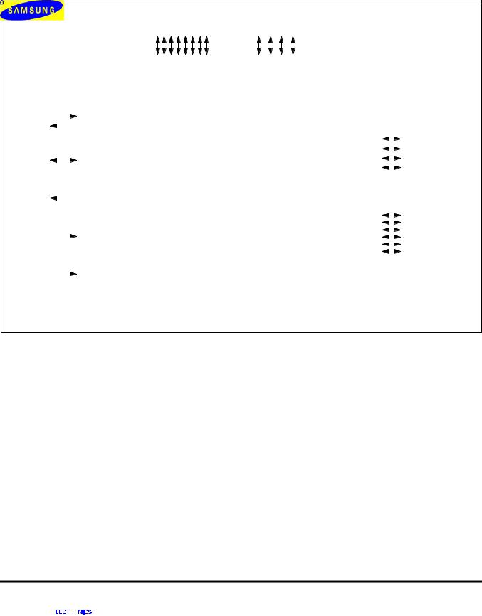
BLOCK DIAGRAM
P1.0-P1.3
P0.0-P0.7 /ZCD,BUZ,T0,CLO
|
|
|
|
|
|
|
|
|
|
PORT 0 |
|
|
|
|
|
PORT 1 |
|
|
|
|
|
|
|||||||||
|
|
|
|
BASIC |
|
|
|
|
|
|
|
|
|
|
|
|
|
|
|
|
|
|
|
||||||||
|
|
|
|
|
|
|
|
|
|
|
|
|
|
|
|
|
|
|
|
|
|
|
|||||||||
XIN |
|
|
|
TIMER |
|
|
|
|
|
|
|
|
|
|
|
|
|
|
|
|
|
|
|
|
|
|
|
|
|
|
|
|
|
|
|
|
|
|
|
|
|
|
|
|
|
|
|
|
|
|
|
|
|
|
|
|
|
|
|
||||
|
|
|
|
|
|
|
|
|
|
|
|
|
|
|
|
|
|
|
|
|
|
|
|
|
|
|
|
|
|
|
|
|
|
|
|
|
|
|
|
|
|
|
|
|
|
|
|
|
|
|
|
|
|
|
|
|
|
|
|
|
|
||
|
|
OSC |
|
|
|
|
|
|
|
|
|
|
|
|
|
|
|
|
|
|
|
|
|
|
|
|
|
|
|
||
XOUT |
|
|
|
|
|
|
|
|
|
|
|
I/O PORT I/O and |
|
|
|
|
|
|
P2.0-P2.3 |
||||||||||||
|
|
|
|
|
|
|
|
|
|
|
|
|
|
|
|
|
|
|
|
||||||||||||
|
|
|
|
|
|
|
|
|
|
|
|
|
|
|
|
|
|
|
|||||||||||||
|
|
|
|
TIMER 0 |
|
|
|
|
|
|
|
INTERRUPT CONTROL |
|
|
|
PORT 2 |
|
|
/INT0-INT1 |
||||||||||||
|
|
|
|
|
|
|
|||||||||||||||||||||||||
|
|
|
|
|
|
|
|
|
|
|
|
|
|
|
|
|
|
|
|
|
|
|
|
|
|
|
|
|
|
||
|
|
|
|
|
|
|
|
|
|
|
|
|
|
|
|
|
|
|
|
|
|
|
|
|
|
|
|
|
|
||
T0(PWM) |
|
|
|
|
|
|
|
|
|
|
|
|
|
|
|
|
|
|
|
|
|
|
|
|
|
/ADC6-ADC7 |
|||||
|
|
|
|
|
|
|
|
|
|
|
|
|
|
|
|
|
|
|
|
|
|
|
|
|
|
|
|
|
|
|
|
|
|
|
|
|
|
|
|
|
|
|
|
|
|
|
|
|
|
|
|
|
|
|
|
|
|
|
|
|
|
|
|
P1.1/BUZ |
|
|
TIMER 1 |
|
|
|
|
|
|
|
|
|
SAM87RI CPU |
|
|
|
|
|
|
P3.0-P3.5 |
|||||||||||
|
|
|
|
|
|
|
|
|
|
|
|
|
|
|
|
||||||||||||||||
|
|
|
|
|
|
|
|
|
|
|
|
|
|
|
|
||||||||||||||||
|
|
|
|
|
|
|
|
|
|
|
|
|
|
|
|
|
|
|
|
||||||||||||
|
|
|
|
|
|
|
|
|
|
|
|
|
|
|
|
|
|
|
|
||||||||||||
|
|
|
|
|
|
|
|
|
|
|
|
|
|
|
|
|
|
|
|
||||||||||||
ADC0 |
|
|
ADC |
|
|
|
|
|
|
|
|
|
|
|
|
|
|
|
|
|
|
|
|
|
|
|
PORT 3 |
|
|
||
|
|
|
|
|
|
|
|
|
|
|
|
|
|
|
|
|
|
|
|
|
|
|
|
|
|||||||
|
|
|
|
|
|
|
|
|
|
|
|
|
|
|
|
|
|
|
|
|
|
|
|||||||||
-ADC7 |
|
|
|
|
|
|
|
|
|
|
|
|
|
|
|
|
|
|
|
|
|
|
|
|
|
|
|
/ADC0-ADC5 |
|||
P1.0/ |
|
|
|
|
|
|
|
|
|
|
|
|
|
|
|
|
|
|
|
|
|
|
|
|
|
|
|
|
|
|
|
|
|
|
|
|
|
|
|
|
|
|
|
|
|
|
|
|
|
|
|
|
|
|
|
|
|
|
|
|
|
|
|
|
|
|
|
|
|
|
|
|
|
|
|
|
|
|
|
|
|
|
|
|
|
|
|
|
|
|
|
|
|
|
|
|
|
|
|
|
|
|
|
|
|
|
|
|
|
|
|
|
|
|
|
|
|
|
|
|
|
|
|
|
|
|
|
|
|
ZCD |
|
|
|
|
|
|
|
|
|
|
|
|
|
|
|
|
|
|
|
|
|
|
|
|
|
|
|
||
|
|
|
|
|
|
|
|
|
|
|
|
|
|
|
|
|
|
|
|
|
|
|
|
|
|
|
|||||
ZCD |
|
|
|
|
|
|
|
|
|
|
|
|
|
|
|
208-BYTE |
|
|
|
|
|
|
|
|
|||||||
|
|
|
|
|
|
|
|
|
|
|
|
|
|
|
|
|
|
|
|
|
|
|
|
||||||||
|
|
|
|
|
|
|
|
|
|
4-KB ROM |
|
|
|
|
|
|
|
|
|
|
|
||||||||||
|
|
|
|
|
|
|
|
|
|
|
|
|
REGISTER FILE |
|
|
|
|
|
|
|
|
||||||||||
|
|
|
|
|
|
|
|
|
|
|
|
|
|
|
|
|
|
|
|
|
|
|
|
|
|
||||||
|
|
|
|
|
|
|
|
|
|
|
|
|
|
|
|
|
|
|
|
|
|
|
|
|
|
|
|
|
|
|
|
Figure 1-1. Block Diagram
1-3
PRODUCT OVERVIEW |
S3C9404/P9404/C9414/P9414 |
|
|
PIN ASSIGNMENTS
|
|
|
|
|
|
|
|
VSS |
|
1 |
|
30 |
|
VDD |
|
|
|
|
|
||||
|
|
|
|
||||
XIN |
|
2 |
|
29 |
|
P0.2 |
|
|
|
|
|
||||
XOUT |
|
3 |
|
28 |
|
P0.3 |
|
|
|
|
|
||||
TEST |
|
4 |
|
27 |
|
P0.4 |
|
|
|
|
|
||||
P0.1 |
|
5 |
|
26 |
|
P0.5 |
|
|
|
|
|
||||
|
|
|
|
||||
P0.0 |
|
6 |
|
25 |
|
P0.6 |
|
|
|
|
|
||||
|
|
|
|
||||
RESET |
|
7 |
S3C9404 |
24 |
|
P0.7 |
|
|
|
|
|||||
|
|
|
|||||
P3.5/ADC5 |
|
8 |
30-SDIP |
23 |
|
P1.0 |
/ ZCD |
P3.4/ADC4 |
|
9 |
22 |
|
P1.1 |
/ BUZ |
|
|
|
||||||
|
(Top View) |
|
|||||
P3.3/ADC3 |
|
10 |
21 |
|
P1.2 / T0(PWM) |
||
|
|
||||||
|
|
|
|||||
P3.2/ADC2 |
|
11 |
|
20 |
|
P1.3 |
/ CLO |
|
|
|
|||||
|
|
|
|||||
P3.1/ADC1 |
|
12 |
|
19 |
|
P2.0 |
/ INT0 |
|
|
|
|||||
|
|
|
|||||
P3.0/ADC0 |
|
13 |
|
18 |
|
P2.1 |
/ INT1 |
|
|
|
|||||
|
|
|
|||||
AVSS |
|
14 |
|
17 |
|
P2.2 |
/ ADC6 |
|
|
|
|||||
|
|
|
|||||
AVref |
|
15 |
|
16 |
|
P2.3 |
/ ADC7 |
|
|
|
|||||
|
|
|
|
|
|
|
|
|
|
|
|
|
|
|
|
Figure 1-2. Pin Assignment Diagram (30-Pin SDIP Package)
VSS |
|
1 |
|
32 |
|
VDD |
|
|
|
|
|
||||
|
|
|
|
||||
XIN |
|
2 |
|
31 |
|
P0.2 |
|
|
|
|
|
||||
|
|
|
|
||||
XOUT |
|
3 |
|
30 |
|
P0.3 |
|
|
|
|
|
||||
|
|
|
|
||||
TEST |
|
4 |
|
29 |
|
P0.4 |
|
|
|
|
|
||||
|
|
|
|
||||
P0.1 |
|
5 |
S3C9404 |
28 |
|
P0.5 |
|
|
|
|
|||||
|
|
|
|||||
P0.0 |
|
6 |
27 |
|
P0.6 |
|
|
|
|
|
|||||
|
32-SOP |
|
|
||||
RESET |
|
7 |
26 |
|
P0.7 |
|
|
|
|
|
|||||
|
|
|
|||||
NC |
|
8 |
(Top View) |
25 |
|
NC |
|
|
|
|
|||||
|
|
|
|||||
P3.5/ADC5 |
|
9 |
|
24 |
|
P1.0 |
/ ZCD |
|
|
|
|||||
|
|
|
|||||
P3.4/ADC4 |
|
10 |
|
23 |
|
P1.1 |
/ BUZ |
|
|
|
|||||
|
|
|
|||||
P3.3/ADC3 |
|
11 |
|
22 |
|
P1.2 / T0(PWM) |
|
|
|
|
|||||
|
|
|
|||||
P3.2/ADC2 |
|
12 |
|
21 |
|
P1.3 |
/ CLO |
|
|
|
|||||
|
|
|
|||||
P3.1/ADC1 |
|
13 |
|
20 |
|
P2.0 / INT0 |
|
|
|
|
|||||
|
|
|
|||||
P3.0/ADC0 |
|
14 |
|
19 |
|
P2.1 / INT1 |
|
|
|
|
|||||
AVSS |
|
15 |
|
18 |
|
P2.2 |
/ ADC6 |
|
|
|
|||||
|
|
|
|||||
AVref |
|
16 |
|
17 |
|
P2.3 |
/ ADC7 |
|
|
|
|||||
|
|
|
|||||
|
|
|
|
|
|
|
|
Figure 1-3. Pin Assignment Diagram (32-Pin SOP Package)
1-4

S3C9404/P9404/C9414/P9414 |
|
PRODUCT OVERVIEW |
|
|
|
|
|
|
|
|
|
VSS |
|
1 |
|
24 |
|
VDD |
|
|
|
||||
|
|
|
||||
XIN |
|
2 |
|
23 |
|
P0.2 |
|
|
|
||||
|
|
|
||||
XOUT |
|
3 |
|
22 |
|
P0.3 |
|
|
|
||||
|
|
|
||||
TEST |
|
4 |
S3C9414 |
21 |
|
P0.4 |
|
|
|||||
|
|
|||||
P0.1 |
|
5 |
20 |
|
P0.5 |
|
|
|
|||||
|
|
|||||
P0.0 |
|
6 |
24-SDIP |
19 |
|
P0.6 |
|
|
|||||
RESET |
|
7 |
18 |
|
P1.0 / ZCD |
|
|
|
|||||
|
(Top View) |
|
||||
|
|
|||||
P3.4/ADC4 |
|
8 |
17 |
|
P1.1 / BUZ |
|
|
|
|||||
|
|
|
||||
P3.3/ADC3 |
|
9 |
|
16 |
|
P1.2 / T0(PWM) |
|
|
|
||||
|
|
|
||||
P3.2/ADC2 |
|
10 |
|
15 |
|
P2.0 / INT0 |
|
|
|
||||
|
|
|
||||
P3.1/ADC1 |
|
11 |
|
14 |
|
AVref |
|
|
|
||||
|
|
|
||||
P3.0/ADC0 |
|
12 |
|
13 |
|
AVSS |
|
|
|
||||
|
|
|
||||
|
|
|
|
|
|
|
Figure 1-4. Pin Assignment Diagram (24-Pin SDIP Package)
VSS |
|
|
|
|
|
|
|
|
|
|
|
|
|
|
|
|
1 |
|
|
24 |
|
VDD |
|
|
|
|
|
||||
|
|
|
|
||||
XIN |
|
2 |
|
|
23 |
|
P0.2 |
|
|
|
|
||||
|
|
|
|
||||
XOUT |
|
3 |
|
|
22 |
|
P0.3 |
|
|
|
|
||||
|
|
|
|
||||
TEST |
|
4 |
|
|
21 |
|
P0.4 |
|
|
|
|
||||
|
|
|
|
||||
P0.1 |
|
5 |
KS86C4104 |
20 |
|
P0.5 |
|
|
|
||||||
|
|
||||||
P0.0 |
|
6 |
|
24-SOP |
19 |
|
P0.6 |
|
|
|
|||||
|
|
|
|||||
RESET |
|
7 |
|
18 |
|
P1.0 / ZCD |
|
|
|
||||||
|
(Top View) |
|
|||||
P3.4/ADC4 |
|
8 |
17 |
|
P1.1 / BUZ |
||
|
|
||||||
|
|
|
|
||||
P3.3/ADC3 |
|
9 |
|
|
16 |
|
P1.2 / T0(PWM) |
|
|
|
|
||||
|
|
|
|
||||
P3.2/ADC2 |
|
10 |
|
|
15 |
|
P2.0 / INT0 |
|
|
|
|
||||
|
|
|
|
||||
P3.1/ADC1 |
|
11 |
|
|
14 |
|
AVref |
|
|
|
|
||||
|
|
|
|
||||
P3.0/ADC0 |
|
12 |
|
|
13 |
|
AVSS |
|
|
|
|
||||
|
|
|
|
||||
|
|
|
|
|
|
|
|
|
|
|
|
|
|
|
|
Figure 1-5. Pin Assignment Diagram (24-Pin SOP Package)
1-5

PRODUCT OVERVIEW S3C9404/P9404/C9414/P9414
PIN DESCRIPTIONS
Table 1-1. S3C9404/C9414 Pin Descriptions
Pin |
Pin |
Pin |
Circuit |
Share |
Names |
Type |
Description |
Type |
Pins |
|
|
|
|
|
P0.0-P0.7 |
I/O |
Bit-programmable I/O port for normal input or |
E-2 |
|
|
|
push-pull, open-drain output. Pull-up resistors are |
|
|
|
|
assignable by software. |
|
|
|
|
|
|
|
P1.0-P1.3 |
I/O |
Bit-programmable I/O port for Schmitt trigger |
F |
ZCD |
|
|
input or push-pull output. Pull-up resistors are |
D |
BUZ |
|
|
assignable by software. Port 1 pins can also be |
D |
T0(PWM) |
|
|
used as alternative functions. |
D |
CLO |
|
|
|
|
|
P2.0-P2.3 |
I/O |
Bit-programmable I/O port for Schmitt trigger |
E |
INT0–INT1 |
|
|
input or push-pull, open drain output. Pull up |
E-1 |
ADC6–ADC7 |
|
|
resistors are assignable by software. Port 2 can |
|
|
|
|
also be used as external interrupt, A/D input. |
|
|
|
|
|
|
|
P3.0-P3.5 |
I/O |
Bit-programmable I/O port for Schmitt trigger |
F |
ADC0–ADC5 |
|
|
input or push-pull output. Pull-up resistors are |
|
|
|
|
assignable by software. Port 3 pins can also be |
|
|
|
|
used as A/D converter input. |
|
|
|
|
|
|
|
XIN, XOUT |
– |
Crystal/ceramic, or RC oscillator signal for system |
– |
– |
|
|
clock. |
|
|
|
|
|
|
|
INT0–INT1 |
I |
External interrupt input. |
E |
P2.0–P2.1 |
|
|
|
|
|
RESET |
I |
System RESET signal input pin. |
B |
– |
|
|
|
|
|
TEST |
I |
Test signal input pin (for factory use only: must be |
– |
– |
|
|
connected to VSS) |
|
|
VDD, VSS |
– |
Voltage input pin and ground |
– |
– |
AVREF, AVSS |
– |
A/D converter reference voltage input and ground |
– |
– |
ZCD |
I |
Zero crossing detector input |
F |
P1.0 |
|
|
|
|
|
BUZ |
O |
200 Hz–20 kHz frequency output for buzzer |
D |
P1.1 |
|
|
sound |
|
|
|
|
|
|
|
T0 |
I/O |
Timer 0 capture input or 10-bit PWM output |
D |
P1.2 |
|
|
|
|
|
CLO |
O |
System clock output port |
D |
P1.3 |
|
|
|
|
|
ADC0–ADC7 |
I |
A/D converter input |
F |
P3.0–P3.5 |
|
|
|
E-1 |
P2.2–P2.3 |
NOTE: Port 0.7, P1.3, P2.1–P2.3 and P3.5 is not available in S3C9414/P4104 .
1-6

S3C9404/P9404/C9414/P9414 |
PRODUCT OVERVIEW |
|
|
PIN CIRCUITS
VDD
 P-CHANNEL
IN 
N-CHANNEL
Figure 1-6. Pin Circuit Type A
VDD
PULL-UP
RESISTOR
IN
Figure 1-7. Pin Circuit Type B
VDD


 P-CHANNEL DATA


 OUT
OUT
N-CHANNEL
OUTPUT
DISABLE
Figure 1-8. Pin Circuit Type C
VDD
PULL-UP
RESISTOR
RESISTOR
P-CHANNEL
ENABLE
DATA
CIRCUIT
IN/OUT
OUTPUT TYPE C DISABLE
DATA 
Figure 1-9. Pin Circuit Type D
1-7

PRODUCT OVERVIEW |
|
|
S3C9404/P9404/C9414/P9414 |
|
VDD |
|
VDD |
|
|
VDD |
|
|
VDD |
|
|
PULL-UP |
|
|
PULL-UP |
PNE |
RESISTOR |
PNE |
|
RESISTOR |
P-CH |
PULL-UP |
|
P-CH |
PULL-UP |
|
ENABLE |
|
|
ENABLE |
DATA |
IN/OUT |
DATA |
|
IN/OUT |
N-CH |
|
|
N-CH |
|
OUTPUT |
|
OUTPUT |
|
|
DISABLE |
|
DISABLE |
|
|
INPUT |
|
INPUT |
|
|
Figure 1-10. Pin Circuit Type E |
Figure 1-10. Pin Circuit Type E-2 |
|||
VDD |
|
|
|
|
VDD |
|
|
VDD |
|
|
|
|
|
|
|
PULL-UP |
|
|
PULL-UP |
PNE |
RESISTOR |
|
|
|
|
|
|
|
RESISTOR |
|
|
PULL-UP |
|
|
P-CH |
PULL-UP |
ENABLE |
|
|
|
ENABLE |
|
VDD |
|
|
|
|
|
|
DATA |
IN/OUT |
DATA |
CIRCUIT |
|
|
IN/OUT |
|||
N-CH |
|
OUTPUT |
TYPE C |
|
|
|
|||
|
DISABLE |
|
|
|
OUTPUT |
|
|
|
|
|
|
|
|
|
DISABLE |
|
DIGITAL |
|
|
|
|
|
|
|
|
|
INPUT |
|
|
DIGITAL INPUT |
|
ANALOG |
|
|
|
|
|
|
|
|
|
INPUT |
|
|
ANALOG INPUT |
|
|
|
|
Figure 1-11. Pin Circuit Type E-1 |
Figure 1-12. Pin Circuit Type F |
|||
1-8

S3C9404/P9404/C9414/P9414 |
ELECTRICAL DATA |
|
|
13 ELECTRICAL DATA
OVERVIEW
In this section, the following S3C9404/C9414 electrical characteristics are presented in tables and graphs:
—Absolute maximum ratings
—D.C. electrical characteristics
—A.C. electrical characteristics
—Oscillator characteristics
—Oscillation stabilization time
—Operating Voltage Range
—Schmitt trigger input characteristics
—Data retention supply voltage in Stop mode
—Stop mode release timing when initiated by a RESET
—A/D converter electrical characteristics
—Zero-crossing detector
—Zero Crossing Waveform Diagram
13-1

ELECTRICAL DATA S3C9404/P9404/C9414/P9414
Table 13-1. Absolute Maximum Ratings
(TA = 25°C)
Parameter |
Symbol |
Conditions |
|
|
Rating |
Unit |
|
|
|
|
|
|
|
|
|
Supply voltage |
VDD |
– |
– 0.3 |
to |
+ 6.5 |
V |
|
Input voltage |
VI |
All input ports |
– 0.3 |
to |
VDD + 0.3 |
V |
|
Output voltage |
VO |
All output ports |
– 0.3 |
to |
VDD + 0.3 |
V |
|
Output current |
IOH |
One I/O pin active |
– 18 |
|
|
|
mA |
high |
|
All I/O pins active |
– 60 |
|
|
|
|
|
|
|
|
|
|
|
|
Output current |
IOL |
One I/O pin active |
+ 30 |
|
|
mA |
|
low |
|
Total pin current for ports 1, 2, 3 |
+ 100 |
|
|
|
|
|
|
|
|
|
|
|
|
|
|
Total pin current for ports 0 |
+ 200 |
|
|
|
|
|
|
|
|
|
|
||
Operating |
TA |
– |
– 40 |
to + 85 |
°C |
||
temperature |
|
|
|
|
|
|
|
|
|
|
|
|
|
||
Storage |
TSTG |
– |
– 65 |
to + 150 |
°C |
||
temperature |
|
|
|
|
|
|
|
|
|
|
|
|
|
|
|
|
|
|
|
Table 13-2. DC Electrical Characteristics |
|
|
|
|||||
(TA = – 40°C to + 85°C, VDD = |
2.7 V to 5.5 V) |
|
|
|
|
|
|
|||||
|
Parameter |
Symbol |
|
|
Conditions |
|
Min |
Typ |
Max |
Unit |
||
|
|
|
|
|
|
|
|
|
||||
|
Input high |
VIH1 |
Ports 1,2,3, and |
VDD= 2.7 to 5.5 V |
0.8 VDD |
– |
VDD |
V |
||||
|
voltage |
|
RESET |
|
|
|
|
|
|
|
||
|
|
VIH2 |
Port 0 |
|
|
0.7 V |
|
|
|
|||
|
|
|
|
|
|
|
|
|
DD |
|
|
|
|
|
|
|
|
|
|
|
|
|
|
|
|
|
|
VIH3 |
X |
and X |
|
V |
DD |
–0.1 |
|
|
|
|
|
|
|
IN |
|
OUT |
|
|
|
|
|
|
|
|
|
|
|
|
|
|
|
|
|
|||
|
Input low |
VIL1 |
Ports 1,2,3, and |
VDD= 2.7 to 5.5 V |
|
– |
– |
0.2 VDD |
V |
|||
|
voltage |
|
RESET |
|
|
|
|
|
|
|
||
|
|
VIL2 |
Port 0 |
|
|
|
|
|
|
0.3 VDD |
|
|
|
|
|
|
|
|
|
|
|
|
|
|
|
|
|
VIL3 |
X |
and X |
|
|
|
|
|
0.1 |
|
|
|
|
|
IN |
|
OUT |
|
|
|
|
|
|
|
|
|
|
|
|
|
|
|
|
||||
|
Output high |
VOH |
IOH = – 1 mA |
VDD= 4.5 to 5.5 V |
VDD – 1.0 |
– |
– |
V |
||||
|
voltage |
|
ports 0, 1, 2, 3 |
|
|
|
|
|
|
|
||
|
|
|
|
|
|
|
|
|
|
|
||
|
Output low |
VOL1 |
IOL = |
15 mA |
VDD= 4.5 to 5.5 V |
|
– |
0.4 |
2.0 |
V |
||
|
voltage |
|
port 0 |
|
|
|
|
|
|
|
|
|
|
|
|
|
|
|
|
|
|
|
|
|
|
|
|
VOL2 |
IOL = |
4 mA |
VDD= 4.5 to 5.5 V |
|
|
|
0.4 |
2.0 |
|
|
|
|
|
port 1,2,3 |
|
|
|
|
|
|
|
||
|
|
|
|
|
|
|
|
|
|
|
|
|
13-2
 Loading...