


Samsung S3C8245, S3C8247, S3C8248, S3C8249, S3P8245 Datasheet
...S3C8248/C8245/P8245/C8247/C8249/P8249 |
PRODUCT OVERVIEW |
|
|
1 PRODUCT OVERVIEW
S3C8-SERIES MICROCONTROLLERS
Samsung's S3C8 series of 8-bit single-chip CMOS microcontrollers offers a fast and efficient CPU, a wide range of integrated peripherals, and various mask-programmable ROM sizes. Among the major CPU features are:
—Efficient register-oriented architecture
—Selectable CPU clock sources
—Idle and Stop power-down mode release by interrupt
—Built-in basic timer with watchdog function
A sophisticated interrupt structure recognizes up to eight interrupt levels. Each level can have one or more interrupt sources and vectors. Fast interrupt processing (within a minimum of four CPU clocks) can be assigned to specific interrupt levels.
S3C8248/C8245/P8245/C8247/C8249/P8249 MICROCONTROLLER
The S3C8248/C8245/P8245/C8247/C8249/P8249 single-chip CMOS microcontroller are fabricated using the highly advanced CMOS process, based on Samsung’s newest CPU architecture.
The S3C8248, S3C8245, S3C8247, S3C8249 are a microcontroller with a 8K-byte, 16K-byte, 24K-byte. 32K-byte mask-programmable ROM embedded respectively.
The S3P8245 is a microcontroller with a 16K-byte one-time-programmable ROM embedded.
The S3P8249 is a microcontroller with a 32K-byte one-time-programmable ROM embedded.
Using a proven modular design approach, Samsung engineers have successfully developed the S3C8248/C8245/P8245/C8247/C8249/P8249 by integrating the following peripheral modules with the powerful SAM8 core:
—Six programmable I/O ports, including five 8-bit ports and one 5-bit port, for a total of 45 pins.
—Eight bit-programmable pins for external interrupts.
—One 8-bit basic timer for oscillation stabilization and watchdog functions (system reset).
—Two 8-bit timer/counter and two 16-bit timer/counter with selectable operating modes.
—Watch timer for real time.
—8-input A/D converter
—Serial I/O interface
The S3C8248/C8245/P8245/C8247/C8249/P8249 is versatile microcontroller for camera, LCD and ADC application, etc. They are currently available in 80-pin TQFP and 80-pin QFP package
OTP
The S3P8245/P8249 are OTP (One Time Programmable) version of the S3C8245/C8249 microcontroller. The S3P8245 microcontroller has an on-chip 16K-byte one-time-programmable EPROM instead of a masked ROM. The S3P8249 microcontroller has an on-chip 32K-byte one-time-programmable EPROM instead of a masked ROM. The S3P8245 is comparable to the S3P8245, both in function and in pin configuration.
The S3P8249 is comparable to the S3P8249, both in function and in pin configuration.
1-1

PRODUCT OVERVIEW |
S3C8248/C8245/P8245/C8247/C8249/P8249 |
|
|
FEATURES
Memory
•ROM: 32K-byte (S3C8249/P8249)
•ROM: 16K-byte (S3C8245/P8245)
•RAM: 1056-Byte (S3C8249/P8249, S3C8247)
•RAM: 544-Byte (S3C8245/P8245, S3C8248)
•Data memory mapped I/O
Oscillation Sources
•Crystal, ceramic, RC (main)
•Crystal for subsystem clock
•Main system clock frequency 1-10 MHz (3 MHz at 1.8 V, 10 MHz at 2.7 V)
•Subsystem clock frequency: 32.768 kHz
•CPU clock divider (1/1, 1/2, 1/8, 1/16)
Two Power-Down Modes
•Idle (only CPU clock stops)
•Stop (System clock stops)
Interrupts
•6 level 8 vector 8 internal interrupt
•2 level 8 vector 8 external interrupt
Watch Timer
•Real-time and interval time measurement
•Clock generation for LCD
•Four frequency outputs for buzzer sound
LCD Controller/Driver
•Maximum 16-digit LCD direct drive capability
•Display modes: static, 1/2 duty (1/2 bias)
•1/3 duty (1/2 or 1/3 bias), 1/4 duty (1/3 bias)
A/D Converter
•Eight analog input channels
•50 μs conversion speed at 1 MHz fADC clock
•10-bit conversion resolution
8-Bit Serial I/O Interface
•8-bit transmit/receive mode
•8-bit receive mode
•LSB-first/MSB-first transmission selectable
•Internal/external clock source
Voltage Booster
•LCD display voltage supply
•S/W control en/disable
•3.0 V drive
45 I/O Pins
•45 configurable I/O pins
Basic Timer
•Overflow signal makes a system reset.
•Watchdog function
8-Bit Timer/Counter A
•Programmable 8-bit timer
•Interval, capture, PWM mode
•Match/capture, overflow interrupt
8-Bit Timer/Counter B
•Programmable 8-bit timer
•Carrier frequency generator
16-Bit Timer/Counter 0
•Programmable 16-bit timer
•Match interrupt generates
16-Bit Timer/Counter 1
•Programmable 16-bit timer
•Interval, capture, PWM mode
•Match/capture, overflow interrupt
Voltage Detector
•Programmable detection voltage (2.2 V, 2.4 V, 3.0 V, 4.0 V)
•En/Disable S/W selectable
Instruction Execution Times
•400 ns at 10 MHz (main)
•122 us at 32.768 kHz (subsystem)
Operating Temperature Range
•-40 °C to 85 °C
Operating Voltage Range
•1.8 V to 5.5 V
Package Type
•80-pin QFP
•80-pin TQFP
S3C8249’s ROM version device
•S3C8247 (ROM 24K-byte)
S3C8245’s ROM version device
•S3C8248 (ROM 8K-byte)
1-2

S3C8248/C8245/P8245/C8247/C8249/P8249 |
PRODUCT OVERVIEW |
|
|
BLOCK DIAGRAM
TAOUT/TAPWM/P3.1  TACLK/P3.2
  TACAP/P3.3
TBPWM/P3.0 
T1CAP/P1.0  T1CLK/P1.1
T1OUT/T1PWM/P1.2 
P0.0-P0.7/
INT0-INT7
P1.0-P1.7

AVREF
AVSS 
P2.0-P2.7/
ADC0-ADC7
P3.0-P3.4

|
|
|
|
XIN XTIN |
|
|
|
|
|
|
|
BUZ/P1.4 |
|
|
|
|
|
|
|
|
|
|
|||||||||||||||
|
RESET |
|
|
|
|
|
|
|
|
|
|
|
|
|
|
|
|
|
|
|
|
|
|
|
|
||||||||||||
8-Bit |
|
|
|
XOUT XTOUT |
|
|
|
|
|
|
|
|
|
|
|||||||||||||||||||||||
|
|
|
|
|
|
|
|
|
|
|
|
|
|
|
|
|
|||||||||||||||||||||
Timer/ |
|
|
|
|
|
|
|
|
|
|
|
|
|
|
|
|
|
|
|
|
|
|
|
|
|
|
|
|
|
|
|
|
|
|
|
|
|
Counter A |
|
|
|
|
|
|
|
|
|
|
|
|
|
|
|
|
|
|
|
|
|
|
|
|
|
|
|
|
|
|
Voltage |
|
|
|
VVLDREF |
||
|
|
|
|
|
|
|
|
|
|
|
|
|
|
|
|
|
|
|
|
|
|
|
|
|
|
|
|
|
|
|
Detector |
|
|
|
|||
|
|
|
|
|
|
|
|
|
|
|
|
|
|
|
|
|
|
|
|
|
|
|
|
|
|
|
|
|
|
|
|
|
|
|
|||
|
|
|
|
|
|
|
|
|
|
|
|
|
|
|
|
|
|
|
|
|
|
|
|
|
|
|
|
|
|
|
|
|
|
|
|
|
|
8-Bit |
|
|
|
|
OSC/ |
|
|
|
Basic |
|
|
|
|
Watch |
|
|
|
|
|
|
|
|
|
|
|||||||||||||
Timer/ |
|
|
|
|
|
|
|
|
|
|
|
|
|
|
Voltage |
|
|
|
CB |
||||||||||||||||||
|
|
|
RESET |
|
|
|
Timer |
|
|
|
|
Timer |
|
|
|
|
|
|
|||||||||||||||||||
Counter B |
|
|
|
|
|
|
|
|
|
|
|
|
|
|
|
|
|
||||||||||||||||||||
|
|
|
|
|
|
|
|
|
|
|
|
|
|
|
|
|
|
|
|
|
|
|
|
|
|
|
|
|
|
Booster |
|
|
|
CA |
|||
|
|
|
|
|
|
|
|
|
|
|
|
|
|
|
|
|
|
|
|
|
|
|
|
|
|
|
|
|
|
|
|
|
|
|
|
|
|
16-Bit |
|
|
|
|
|
|
|
|
|
|
|
|
|
|
|
|
|
|
|
|
|
|
|
|
|
|
|
|
|
|
|
|
|
|
|
|
|
|
|
|
|
|
|
|
|
|
|
|
|
|
|
|
|
|
|
|
|
|
|
|
|
|
|
|
|
|
|
|
|
|
|
|
|
|
|
Timer/ |
|
|
|
|
|
|
|
|
|
|
|
|
|
|
|
|
|
|
|
|
|
|
|
|
|
|
|
|
|
|
|
|
|
|
|
|
|
Counter 0 |
|
|
|
|
|
|
|
|
|
|
|
|
|
|
|
|
|
|
|
|
|
|
|
|
|
|
|
|
|
|
|
|
|
|
|
|
VLC0-VLC2 |
|
|
|
|
|
|
|
|
|
|
|
|
|
|
|
|
|
|
|
|
|
|
|
|
|
|
|
|
|
|
|
|
|
|
|
|
|
|
|
|
|
|
|
|
|
|
|
|
|
|
|
|
|
|
|
|
|
|
|
|
|
|
|
|
|
|
|
|
|
|
|
|
|
|
|
|
|
|
|
|
|
|
|
|
|
|
|
|
|
|
|
|
|
|
|
|
|
|
|
|
|
|
|
|
|
|
|
LCD |
|
|
|
COM0-COM3 |
||
16-Bit |
|
|
|
|
|
|
|
|
|
|
|
|
|
|
|
|
|
|
|
|
|
|
|
|
|
|
|
|
|
|
|
|
|
||||
|
|
|
|
|
|
|
|
|
|
|
|
|
|
|
|
|
|
|
|
|
|
|
|
|
|
|
|
|
|
|
|
|
|||||
|
|
|
|
|
|
|
|
|
|
|
|
|
|
|
|
|
|
|
|
|
|
|
|
|
|
|
|
|
|
|
|
|
|
||||
Timer/ |
|
|
|
|
|
|
|
I/O Port and Interrupt Control |
|
|
|
Driver |
|
|
|
SEG0-SEG15 |
|||||||||||||||||||||
|
|
|
|
|
|
|
|
|
|
|
|||||||||||||||||||||||||||
|
|
|
|
|
|
|
|
|
|
|
|
|
|||||||||||||||||||||||||
Counter 1 |
|
|
|
|
|
|
|
|
|
|
|
|
|
|
|
|
|
|
|
|
|
|
|
|
|
|
|
|
|
|
|
|
|
|
|
|
SEG16-SEG31 |
|
|
|
|
|
|
|
|
|
|
|
|
|
|
|
|
|
|
|
|
|
|
|
|
|
|
|
|
|
|
|
|
|
|
|
|
|
|
|
|
|
|
|
|
|
|
|
|
|
|
|
|
|
|
|
|
|
|
|
|
|
|
|
|
|
|
|
|
|
|
|
|
|
|
|
|
|
|
|
|
|
|
|
|
|
|
|
|
|
|
|
|
|
|
|
|
|
|
|
|
|
|
|
|
|
|
|
|
|
|
|
|
|
|
I/O Port 0 |
|
|
|
|
|
|
|
|
|
|
|
|
|
|
|
|
|
|
|
|
|
|
|
|
|
|
|
|
|
|
|
|
|
|
|
|
|
|
|
|
|
|
|
|
|
|
|
|
|
|
|
|
|
|
|
|
|
|
|
|
|
|
|
|
|
|
|
|
|
|
|
|
|
|
|
|
|
|
|
|
|
|
|
|
|
|
|
|
|
|
|
|
|
|
|
|
|
|
|
|
|||||||||||||
I/O Port 1 |
|
|
|
|
|
|
|
|
|
|
|
SAM88 RC CPU |
|
|
|
|
|
|
|
|
|
SI/P1.7 |
|||||||||||||||
|
|
|
|
|
|
|
|
|
|
|
|
|
|
|
|
|
|
|
|
||||||||||||||||||
|
|
|
|
|
|
|
|
|
|
|
|
|
|
Serial I/O |
|
|
|
||||||||||||||||||||
|
|
|
|
|
|
|
|
|
|
|
|
|
|
|
|
|
|
|
|
|
|
|
|
|
|
|
|
|
|
|
Port |
|
|
|
SO/P1.5 |
||
A/D |
|
|
|
|
|
|
|
|
|
|
|
|
|
|
|
|
|
|
|
|
|
|
|
|
|
|
|
|
|
|
|
|
|
|
|
|
SCK/P1.6 |
|
|
|
|
|
|
|
|
|
|
|
|
|
|
|
|
|
|
|
|
|
|
|
|
|
|
|
|
|
|
|
|
|
|
|
|
|
|
Converter |
|
|
|
|
|
|
|
|
|
|
|
|
|
|
|
|
|
|
|
|
|
|
|
|
|
|
|
|
|
|
|
|
|
|
|
|
|
|
|
|
|
|
|
|
|
|
|
|
|
|
|
|
|
|
|
|
|
|
|
|
|
|
|
|
|
|
|
|
|
|
|
|
|
|
|
I/O Port 2 |
|
|
|
544/1056 Byte |
|
|
|
|
|
16/32-Kbyte |
|
|
|
|
I/O Port 4 |
|
|
|
P4.0-P4.7 |
||||||||||||||||||
|
|
|
|
|
|
|
|
|
|
|
|
|
|
|
|
|
|
|
|||||||||||||||||||
|
|
|
|
|
|
|
|
|
|
|
|
|
|
|
|
|
|
|
|||||||||||||||||||
|
|
|
|
|
Register File |
|
|
|
|
|
|
ROM |
|
|
|
|
|
|
|
|
|
|
|
||||||||||||||
|
|
|
|
|
|
|
|
|
|
|
|
|
|
|
|
|
|
|
|
|
|||||||||||||||||
|
|
|
|
|
|
|
|
|
|
|
|
|
|
|
|
|
|
|
|
|
|
|
|
|
|
|
|
|
|
|
|
|
|
|
|
|
|
I/O Port 3 |
|
|
|
|
|
|
|
|
|
|
|
|
|
|
|
|
|
|
|
|
|
|
|
|
|
|
|
|
|
|
I/O Port 5 |
|
|
|
P5.0-P5.7 |
||
|
|
|
|
|
|
|
|
|
|
|
|
|
|
|
|
|
|
|
|
|
|
|
|
|
|
|
|
|
|
|
|
|
|||||
|
|
|
|
|
|
|
|
|
|
|
|
|
|
|
|
|
|
|
|
|
|
|
|
|
|
|
|
|
|
|
|
|
|
|
|
|
|
Figure 1-1. Block Diagram
1-3
PRODUCT OVERVIEW |
S3C8248/C8245/P8245/C8247/C8249/P8249 |
|
|
PIN ASSIGNMENT
|
|
|
|
SEG25/P5.1 |
|
SEG24/P5.0 |
|
SEG23/P4.7 |
|
SEG22/P4.6 |
|
SEG21/P4.5 |
|
SEG20/P4.4 |
|
SEG19/P4.3 |
|
SEG18/P4.2 |
|
SEG17/P4.1 |
|
SEG16/P4.0 |
|
SEG15 |
|
SEG14 |
|
SEG13 |
|
SEG12 |
|
SEG11 |
|
SEG10 |
|
|
||||||||||||||||
|
|
|
|
|
|
|
|
|
|
|
|
|
|
|
|
|
|
|
|
|
|
|
|
|
|
|
|
|
|
|
|
|
|
|
|
|
|
|
|
|
|
|
|
|
|
|
|
|
|
|
|
|
|
|
|
|
|
|
|
|
|
|
|
|
|
|
|
|
|
|
|
|
|
|
|
|
|
|
|
|
|
|
|
|
|
|
|
|
|
|
|
|
|
|
|
|
|
|
|
|
|
|
|
|
|
|
|
|
80 |
79 |
78 |
77 |
76 |
75 |
74 |
73 |
72 |
71 |
70 |
69 |
68 |
67 |
66 |
65 |
|
|
||||||||||||||||||||||||||||||||
SEG26/P5.2 |
|
1 |
|
|
|
|
|
|
|
|
|
|
|
|
|
|
|
|
|
|
|
|
|
|
|
|
|
|
|
|
|
|
|
|
|
|
|
|
|
|
|
|
|
|
|
|
64 |
|
SEG9 |
|||
|
|
|
|
|
|
|
|
|
|
|
|
|
|
|
|
|
|
|
|
|
|
|
|
|
|
|
|
|
|
|
|
|
|
|
|
|
|
|
|
|
|
|
|
|
|
|||||||
|
|
|
|
|
|
|
|
|
|
|
|
|
|
|
|
|
|
|
|
|
|
|
|
|
|
|
|
|
|
|
|
|
|
|
|
|
|
|
|
|
|
|
|
|
|
|||||||
SEG27/P5.3 |
|
2 |
|
|
|
|
|
|
|
|
|
|
|
|
|
|
|
|
|
|
|
|
|
|
|
|
|
|
|
|
|
|
|
|
|
|
|
|
|
|
|
|
|
|
|
|
63 |
|
SEG8 |
|||
|
|
|
|
|
|
|
|
|
|
|
|
|
|
|
|
|
|
|
|
|
|
|
|
|
|
|
|
|
|
|
|
|
|
|
|
|
|
|
|
|
|
|
|
|
|
|||||||
|
|
|
|
|
|
|
|
|
|
|
|
|
|
|
|
|
|
|
|
|
|
|
|
|
|
|
|
|
|
|
|
|
|
|
|
|
|
|
|
|
|
|
|
|
|
|||||||
SEG28/P5.4 |
|
3 |
|
|
|
|
|
|
|
|
|
|
|
|
|
|
|
|
|
|
|
|
|
|
|
|
|
|
|
|
|
|
|
|
|
|
|
|
|
|
|
|
|
|
|
|
62 |
|
SEG7 |
|||
|
|
|
|
|
|
|
|
|
|
|
|
|
|
|
|
|
|
|
|
|
|
|
|
|
|
|
|
|
|
|
|
|
|
|
|
|
|
|
|
|
|
|
|
|
|
|||||||
|
|
|
|
|
|
|
|
|
|
|
|
|
|
|
|
|
|
|
|
|
|
|
|
|
|
|
|
|
|
|
|
|
|
|
|
|
|
|
|
|
|
|
|
|
|
|||||||
SEG29/P5.5 |
|
4 |
|
|
|
|
|
|
|
|
|
|
|
|
|
|
|
|
|
|
|
|
|
|
|
|
|
|
|
|
|
|
|
|
|
|
|
|
|
|
|
|
|
|
|
|
61 |
|
SEG6 |
|||
|
|
|
|
|
|
|
|
|
|
|
|
|
|
|
|
|
|
|
|
|
|
|
|
|
|
|
|
|
|
|
|
|
|
|
|
|
|
|
|
|
|
|
|
|
|
|||||||
|
|
|
|
|
|
|
|
|
|
|
|
|
|
|
|
|
|
|
|
|
|
|
|
|
|
|
|
|
|
|
|
|
|
|
|
|
|
|
|
|
|
|
|
|
|
|||||||
SEG30/P5.6 |
|
5 |
|
|
|
|
|
|
|
|
|
|
|
|
|
|
|
|
|
|
|
|
|
|
|
|
|
|
|
|
|
|
|
|
|
|
|
|
|
|
|
|
|
|
|
|
60 |
|
SEG5 |
|||
|
|
|
|
|
|
|
|
|
|
|
|
|
|
|
|
|
|
|
|
|
|
|
|
|
|
|
|
|
|
|
|
|
|
|
|
|
|
|
|
|
|
|
|
|
|
|||||||
|
|
|
|
|
|
|
|
|
|
|
|
|
|
|
|
|
|
|
|
|
|
|
|
|
|
|
|
|
|
|
|
|
|
|
|
|
|
|
|
|
|
|
|
|
|
|||||||
SEG31/P5.7 |
|
6 |
|
|
|
|
|
|
|
|
|
|
|
|
|
|
|
|
|
|
|
|
|
|
|
|
|
|
|
|
|
|
|
|
|
|
|
|
|
|
|
|
|
|
|
|
59 |
|
SEG4 |
|||
|
|
|
|
|
|
|
|
|
|
|
|
|
|
|
|
|
|
|
|
|
|
|
|
|
|
|
|
|
|
|
|
|
|
|
|
|
|
|
|
|
|
|
|
|
|
|||||||
|
|
|
|
|
|
|
|
|
|
|
|
|
|
|
|
|
|
|
|
|
|
|
|
|
|
|
|
|
|
|
|
|
|
|
|
|
|
|
|
|
|
|
|
|
|
|||||||
P3.0/TBPWM |
|
7 |
|
|
|
|
|
|
|
|
|
|
|
|
|
|
|
|
|
|
|
|
|
|
|
|
|
|
|
|
|
|
|
|
|
|
|
|
|
|
|
|
|
|
|
|
58 |
|
SEG3 |
|||
|
|
|
|
|
|
|
|
|
|
|
|
|
|
|
|
|
|
|
|
|
|
|
|
|
|
|
|
|
|
|
|
|
|
|
|
|
|
|
|
|
|
|
|
|
|
|||||||
|
|
|
|
|
|
|
|
|
|
|
|
|
|
|
|
|
|
|
|
|
|
|
|
|
|
|
|
|
|
|
|
|
|
|
|
|
|
|
|
|
|
|
|
|
|
|||||||
P3.1/TAOUT/TAPWM |
|
8 |
|
|
|
|
|
|
|
|
|
|
|
|
|
|
|
|
|
|
|
|
|
|
|
|
|
|
|
|
|
|
|
|
|
|
|
|
|
|
|
|
|
|
|
|
57 |
|
SEG2 |
|||
|
|
|
|
|
|
|
|
|
|
|
|
|
|
|
|
|
|
|
|
|
|
|
|
|
|
|
|
|
|
|
|
|
|
|
|
|
|
|
|
|
|
|
|
|
|
|||||||
|
|
|
|
|
|
|
|
|
|
|
|
|
|
|
|
|
|
|
|
|
|
|
|
|
|
|
|
|
|
|
|
|
|
|
|
|
|
|
|
|
|
|
|
|
|
|||||||
P3.2/TACLK |
|
9 |
|
|
|
|
|
|
|
|
|
|
|
|
|
|
|
|
|
|
|
|
|
|
|
|
|
|
|
|
|
|
|
|
|
|
|
|
|
|
|
|
|
|
|
|
56 |
|
SEG1 |
|||
|
|
|
|
|
|
|
|
|
|
|
|
|
|
|
|
|
|
|
|
|
|
|
|
|
|
|
|
|
|
|
|
|
|
|
|
|
|
|
|
|
|
|
|
|
|
|||||||
|
|
|
|
|
|
|
|
|
|
|
|
|
|
|
|
|
|
|
|
|
|
|
|
|
|
|
|
|
|
|
|
|
|
|
|
|
|
|
|
|
|
|
|
|
|
|||||||
P3.3/TACAP/SDAT |
|
10 |
|
|
|
|
|
|
|
|
|
S3C8248/C8245 |
|
|
|
|
|
|
55 |
|
SEG0 |
|||||||||||||||||||||||||||||||
|
|
|
|
|
|
|
|
|
|
|
|
|
|
|
|
|
||||||||||||||||||||||||||||||||||||
|
|
|
|
|
|
|
|
|
|
|
|
|
|
|
|
|
||||||||||||||||||||||||||||||||||||
P3.4/SCLK |
|
|
11 |
|
|
|
|
|
|
|
|
|
|
|
|
|
|
|
54 |
|
COM3 |
|||||||||||||||||||||||||||||||
|
|
|
|
|
|
|
|
|
|
|
|
|
|
|
|
|
|
|||||||||||||||||||||||||||||||||||
|
|
|
|
|
|
|
|
|
|
|
|
|
|
|
|
|
|
|||||||||||||||||||||||||||||||||||
VDD |
|
12 |
|
|
|
|
|
|
|
|
|
|
/C8247/C8249 |
|
|
|
|
|
|
|
|
|
53 |
|
COM2 |
|||||||||||||||||||||||||||
|
|
|
|
|
|
|
|
|
|
|
|
|
|
|
|
|
|
|
|
|
|
|||||||||||||||||||||||||||||||
|
|
|
|
|
|
|
|
|
|
|
|
|
|
|
|
|
|
|
|
|
|
|||||||||||||||||||||||||||||||
VSS |
|
|
13 |
|
|
|
|
|
|
|
|
|
|
|
|
|
|
|
|
|
|
|
|
|
|
|
|
|
|
|
|
|
|
|
|
|
|
|
|
|
|
|
|
|
|
|
|
52 |
|
COM1 |
||
|
|
|
|
|
|
|
|
|
|
|
|
|
|
|
|
|
|
|
|
|
|
|
|
|
|
|
|
|
|
|
|
|
|
|
|
|
|
|
|
|
|
|
|
|
|
|
||||||
XOUT |
|
14 |
|
|
|
|
|
|
|
|
|
|
|
|
(80-QFP-1420C) |
|
|
|
|
|
|
|
|
|
51 |
|
COM0 |
|||||||||||||||||||||||||
|
|
|
|
|
|
|
|
|
|
|
|
|
|
|
|
|
|
|
|
|
|
|
|
|||||||||||||||||||||||||||||
|
|
|
|
|
|
|
|
|
|
|
|
|
|
|
|
|
|
|
|
|
|
|
|
|||||||||||||||||||||||||||||
XIN |
|
|
15 |
|
|
|
|
|
|
|
|
|
|
|
|
|
|
|
|
|
|
|
|
|
50 |
|
VLC2 |
|||||||||||||||||||||||||
|
|
|
|
|
|
|
|
|
|
|
|
|
|
|
|
|
|
|
|
|
|
|
|
|||||||||||||||||||||||||||||
|
|
|
|
|
|
|
|
|
|
|
|
|
|
|
|
|
|
|
|
|
|
|
|
|
|
|
|
|
|
|
|
|
|
|
|
|
|
|
|
|
|
|
|
|
|
|||||||
TEST |
|
16 |
|
|
|
|
|
|
|
|
|
|
|
|
|
|
|
|
|
|
|
|
|
|
|
|
|
|
|
|
|
|
|
|
|
|
|
|
|
|
|
|
|
|
|
|
49 |
|
VLC1 |
|||
|
|
|
|
|
|
|
|
|
|
|
|
|
|
|
|
|
|
|
|
|
|
|
|
|
|
|
|
|
|
|
|
|
|
|
|
|
|
|
|
|
|
|
|
|
|
|
||||||
|
|
|
|
|
|
|
|
|
|
|
|
|
|
|
|
|
|
|
|
|
|
|
|
|
|
|
|
|
|
|
|
|
|
|
|
|
|
|
|
|
|
|
|
|
|
|
||||||
XTIN |
|
17 |
|
|
|
|
|
|
|
|
|
|
|
|
|
|
|
|
|
|
|
|
|
|
|
|
|
|
|
|
|
|
|
|
|
|
|
|
|
|
|
|
|
|
|
|
48 |
|
VLC0 |
|||
|
|
|
|
|
|
|
|
|
|
|
|
|
|
|
|
|
|
|
|
|
|
|
|
|
|
|
|
|
|
|
|
|
|
|
|
|
|
|
|
|
|
|
|
|
|
|
||||||
|
|
|
|
|
|
|
|
|
|
|
|
|
|
|
|
|
|
|
|
|
|
|
|
|
|
|
|
|
|
|
|
|
|
|
|
|
|
|
|
|
|
|
|
|
|
|
||||||
XTOUT |
|
18 |
|
|
|
|
|
|
|
|
|
|
|
|
|
|
|
|
|
|
|
|
|
|
|
|
|
|
|
|
|
|
|
|
|
|
|
|
|
|
|
|
|
|
|
|
47 |
|
CA |
|||
|
|
|
|
|
|
|
|
|
|
|
|
|
|
|
|
|
|
|
|
|
|
|
|
|
|
|
|
|
|
|
|
|
|
|
|
|
|
|
|
|
|
|
|
|
|
|
||||||
|
|
|
|
|
|
|
|
|
|
|
|
|
|
|
|
|
|
|
|
|
|
|
|
|
|
|
|
|
|
|
|
|
|
|
|
|
|
|
|
|
|
|
|
|
|
|
||||||
RESET |
|
19 |
|
|
|
|
|
|
|
|
|
|
|
|
|
|
|
|
|
|
|
|
|
|
|
|
|
|
|
|
|
|
|
|
|
|
|
|
|
|
|
|
|
|
|
|
46 |
|
CB |
|||
|
|
|
|
|
|
|
|
|
|
|
|
|
|
|
|
|
|
|
|
|
|
|
|
|
|
|
|
|
|
|
|
|
|
|
|
|
|
|
|
|
|
|
|
|
|
|
||||||
|
|
|
|
|
|
|
|
|
|
|
|
|
|
|
|
|
|
|
|
|
|
|
|
|
|
|
|
|
|
|
|
|
|
|
|
|
|
|
|
|
|
|
|
|
|
|
||||||
P0.0/INT0 |
|
20 |
|
|
|
|
|
|
|
|
|
|
|
|
|
|
|
|
|
|
|
|
|
|
|
|
|
|
|
|
|
|
|
|
|
|
|
|
|
|
|
|
|
|
|
|
45 |
|
AVSS |
|||
|
|
|
|
|
|
|
|
|
|
|
|
|
|
|
|
|
|
|
|
|
|
|
|
|
|
|
|
|
|
|
|
|
|
|
|
|
|
|
|
|
|
|
|
|
|
|
||||||
|
|
|
|
|
|
|
|
|
|
|
|
|
|
|
|
|
|
|
|
|
|
|
|
|
|
|
|
|
|
|
|
|
|
|
|
|
|
|
|
|
|
|
|
|
|
|
||||||
P0.1/INT1 |
|
21 |
|
|
|
|
|
|
|
|
|
|
|
|
|
|
|
|
|
|
|
|
|
|
|
|
|
|
|
|
|
|
|
|
|
|
|
|
|
|
|
|
|
|
|
|
44 |
|
AVREF |
|||
|
|
|
|
|
|
|
|
|
|
|
|
|
|
|
|
|
|
|
|
|
|
|
|
|
|
|
|
|
|
|
|
|
|
|
|
|
|
|
|
|
|
|
|
|
|
|
||||||
|
|
|
|
|
|
|
|
|
|
|
|
|
|
|
|
|
|
|
|
|
|
|
|
|
|
|
|
|
|
|
|
|
|
|
|
|
|
|
|
|
|
|
|
|
|
|
||||||
P0.2/INT2 |
|
22 |
|
|
|
|
|
|
|
|
|
|
|
|
|
|
|
|
|
|
|
|
|
|
|
|
|
|
|
|
|
|
|
|
|
|
|
|
|
|
|
|
|
|
|
|
43 |
|
P2.7/ADC7/VVLDREF |
|||
|
|
|
|
|
|
|
|
|
|
|
|
|
|
|
|
|
|
|
|
|
|
|
|
|
|
|
|
|
|
|
|
|
|
|
|
|
|
|
|
|
|
|
|
|
|
|
||||||
|
|
|
|
|
|
|
|
|
|
|
|
|
|
|
|
|
|
|
|
|
|
|
|
|
|
|
|
|
|
|
|
|
|
|
|
|
|
|
|
|
|
|
|
|
|
|
||||||
P0.3/INT3 |
|
23 |
|
|
|
|
|
|
|
|
|
|
|
|
|
|
|
|
|
|
|
|
|
|
|
|
|
|
|
|
|
|
|
|
|
|
|
|
|
|
|
|
|
|
|
|
42 |
|
P2.6/ADC6 |
|||
|
|
|
|
|
|
|
|
|
|
|
|
|
|
|
|
|
|
|
|
|
|
|
|
|
|
|
|
|
|
|
|
|
|
|
|
|
|
|
|
|
|
|
|
|
|
|
||||||
|
|
|
|
|
|
|
|
|
|
|
|
|
|
|
|
|
|
|
|
|
|
|
|
|
|
|
|
|
|
|
|
|
|
|
|
|
|
|
|
|
|
|
|
|
|
|
||||||
P0.4/INT4 |
|
24 |
|
|
|
|
|
|
|
|
|
|
|
|
|
|
|
|
|
|
|
|
|
|
|
|
|
|
|
|
|
|
|
|
|
|
|
|
|
|
|
|
|
|
|
|
41 |
|
P2.5/ADC5 |
|||
|
|
|
|
|
|
|
|
|
|
|
|
|
|
|
|
|
|
|
|
|
|
|
|
|
|
|
|
|
|
|
|
|
|
|
|
|
|
|
|
|
|
|
|
|
|
|
||||||
|
|
|
|
|
|
|
|
|
|
|
|
|
|
|
|
|
|
|
|
|
|
|
|
|
|
|
|
|
|
|
|
|
|
|
|
|
|
|
|
|
|
|
|
|
|
|
||||||
|
|
|
25 |
|
26 |
|
27 |
|
28 |
|
28 |
|
30 |
|
31 |
|
32 |
|
33 |
|
34 |
|
35 |
|
36 |
|
37 |
|
38 |
|
39 |
|
40 |
|
|
|
||||||||||||||||
|
|
|
|
|
|
|
|
|
|
|
|
|
|
|
|
|
|
|
|
|
|
|
|
|
|
|
|
|
|
|
|
|
|
|
|
|
|
|
|
|
|
|
|
|
|
|
|
|
|
|
|
|
|
|
|
|
|
|
|
|
|
|
|
|
|
|
|
|
|
|
|
|
|
|
|
|
|
|
|
|
|
|
|
|
|
|
|
|
|
|
|
|
|
|
|
|
|
|
|
|
|
|
|
|
|
|
|
|
P0.5/INT5 |
P0.6/INT6 |
P0.7/INT7 |
P1.0/T1CAP |
P1.1/T1CLK |
|
P1.2/T1OUT/T1PWM |
P1.3 |
P1.4/BUZ |
P1.5/SO |
P1.6/SCK |
P1.7/SI |
P2.0/ADC0 |
P2.1/ADC1 |
P2.2/ADC3 |
P2.3/ADC4 |
P2.4/ADC4 |
|
|
|||||||||||||||||||||||||||||||
Figure 1-2. S3C8248/C8245/C8247/C8249 Pin Assignments (80-QFP)
1-4
S3C8248/C8245/P8245/C8247/C8249/P8249 |
PRODUCT OVERVIEW |
|
|
|
|
|
|
SEG25/P5.1 |
|
SEG24/P5.0 |
|
SEG23/P4.7 |
|
SEG22/P4.6 |
|
SEG21/P4.5 |
|
SEG20/P4.4 |
|
SEG19/P4.3 |
|
SEG18/P4.2 |
|
SEG17/P4.1 |
|
SEG16/P4.0 |
|
SEG15 |
|
SEG14 |
|
SEG13 |
|
SEG12 |
|
SEG11 |
|
SEG10 |
|
SEG9 |
|
SEG8 |
|
SEG7 |
|
SEG6 |
|
|
||||||||||||||||||||
|
|
|
|
|
|
|
|
|
|
|
|
|
|
|
|
|
|
|
|
|
|
|
|
|
|
|
|
|
|
|
|
|
|
|
|
|
|
|
|
|
|
|
|
|
|
|
|
|
|
|
|
|
|
|
|
|
|
|
|
|
|
|
|
|
|
|
|
|
|
|
|
|
|
|
|
|
|
|
|
|
|
|
|
|
|
|
|
|
|
|
|
|
|
|
|
|
|
|
|
|
|
|
|
|
|
|
|
|
|
|
|
|
|
|
|
|
|
|
|
|
|
|
|
|
|
|
|
|
|
|
|
|
80 |
79 |
78 |
77 |
76 |
75 |
74 |
73 |
72 |
71 |
70 |
69 |
68 |
67 |
66 |
65 |
64 |
63 |
62 |
61 |
|
|
||||||||||||||||||||||||||||||||||||||||
SEG26/P5.2 |
|
1 |
|
|
|
|
|
|
|
|
|
|
|
|
|
|
|
|
|
|
|
|
|
|
|
|
|
|
|
|
|
|
|
|
|
|
|
|
|
|
|
|
|
|
|
|
|
|
|
|
|
|
|
|
|
|
|
|
60 |
|
SEG5 |
|||
|
|
|
|
|
|
|
|
|
|
|
|
|
|
|
|
|
|
|
|
|
|
|
|
|
|
|
|
|
|
|
|
|
|
|
|
|
|
|
|
|
|
|
|
|
|
|
|
|
|
|
|
|
|
|
|
|
|
|||||||
|
|
|
|
|
|
|
|
|
|
|
|
|
|
|
|
|
|
|
|
|
|
|
|
|
|
|
|
|
|
|
|
|
|
|
|
|
|
|
|
|
|
|
|
|
|
|
|
|
|
|
|
|
|
|
|
|
|
|||||||
SEG27/P5.3 |
|
2 |
|
|
|
|
|
|
|
|
|
|
|
|
|
|
|
|
|
|
|
|
|
|
|
|
|
|
|
|
|
|
|
|
|
|
|
|
|
|
|
|
|
|
|
|
|
|
|
|
|
|
|
|
|
|
|
|
59 |
|
SEG4 |
|||
|
|
|
|
|
|
|
|
|
|
|
|
|
|
|
|
|
|
|
|
|
|
|
|
|
|
|
|
|
|
|
|
|
|
|
|
|
|
|
|
|
|
|
|
|
|
|
|
|
|
|
|
|
|
|
|
|
|
|||||||
|
|
|
|
|
|
|
|
|
|
|
|
|
|
|
|
|
|
|
|
|
|
|
|
|
|
|
|
|
|
|
|
|
|
|
|
|
|
|
|
|
|
|
|
|
|
|
|
|
|
|
|
|
|
|
|
|
|
|||||||
SEG28/P5.4 |
|
3 |
|
|
|
|
|
|
|
|
|
|
|
|
|
|
|
|
|
|
|
|
|
|
|
|
|
|
|
|
|
|
|
|
|
|
|
|
|
|
|
|
|
|
|
|
|
|
|
|
|
|
|
|
|
|
|
|
58 |
|
SEG3 |
|||
|
|
|
|
|
|
|
|
|
|
|
|
|
|
|
|
|
|
|
|
|
|
|
|
|
|
|
|
|
|
|
|
|
|
|
|
|
|
|
|
|
|
|
|
|
|
|
|
|
|
|
|
|
|
|
|
|
|
|||||||
|
|
|
|
|
|
|
|
|
|
|
|
|
|
|
|
|
|
|
|
|
|
|
|
|
|
|
|
|
|
|
|
|
|
|
|
|
|
|
|
|
|
|
|
|
|
|
|
|
|
|
|
|
|
|
|
|
|
|||||||
SEG29/P5.5 |
|
4 |
|
|
|
|
|
|
|
|
|
|
|
|
|
|
|
|
|
|
|
|
|
|
|
|
|
|
|
|
|
|
|
|
|
|
|
|
|
|
|
|
|
|
|
|
|
|
|
|
|
|
|
|
|
|
|
|
57 |
|
SEG2 |
|||
|
|
|
|
|
|
|
|
|
|
|
|
|
|
|
|
|
|
|
|
|
|
|
|
|
|
|
|
|
|
|
|
|
|
|
|
|
|
|
|
|
|
|
|
|
|
|
|
|
|
|
|
|
|
|
|
|
|
|||||||
|
|
|
|
|
|
|
|
|
|
|
|
|
|
|
|
|
|
|
|
|
|
|
|
|
|
|
|
|
|
|
|
|
|
|
|
|
|
|
|
|
|
|
|
|
|
|
|
|
|
|
|
|
|
|
|
|
|
|||||||
SEG30/P5.6 |
|
5 |
|
|
|
|
|
|
|
|
|
|
|
|
|
|
|
|
|
|
|
|
|
|
|
|
|
|
|
|
|
|
|
|
|
|
|
|
|
|
|
|
|
|
|
|
|
|
|
|
|
|
|
|
|
|
|
|
56 |
|
SEG1 |
|||
|
|
|
|
|
|
|
|
|
|
|
|
|
|
|
|
|
|
|
|
|
|
|
|
|
|
|
|
|
|
|
|
|
|
|
|
|
|
|
|
|
|
|
|
|
|
|
|
|
|
|
|
|
|
|
|
|
|
|||||||
|
|
|
|
|
|
|
|
|
|
|
|
|
|
|
|
|
|
|
|
|
|
|
|
|
|
|
|
|
|
|
|
|
|
|
|
|
|
|
|
|
|
|
|
|
|
|
|
|
|
|
|
|
|
|
|
|
|
|||||||
SEG31/P5.7 |
|
6 |
|
|
|
|
|
|
|
|
|
|
|
|
|
|
|
|
|
|
|
|
|
|
|
|
|
|
|
|
|
|
|
|
|
|
|
|
|
|
|
|
|
|
|
|
|
|
|
|
|
|
|
|
|
|
|
|
55 |
|
SEG0 |
|||
|
|
|
|
|
|
|
|
|
|
|
|
|
|
|
|
|
|
|
|
|
|
|
|
|
|
|
|
|
|
|
|
|
|
|
|
|
|
|
|
|
|
|
|
|
|
|
|
|
|
|
|
|
|
|
|
|
|
|||||||
|
|
|
|
|
|
|
|
|
|
|
|
|
|
|
|
|
|
|
|
|
|
|
|
|
|
|
|
|
|
|
|
|
|
|
|
|
|
|
|
|
|
|
|
|
|
|
|
|
|
|
|
|
|
|
|
|
|
|||||||
P3.0/TBPWM |
|
7 |
|
|
|
|
|
|
|
|
|
|
|
|
|
|
|
|
|
|
|
|
|
|
|
|
|
|
|
|
|
|
|
|
|
|
|
|
|
|
|
|
|
|
|
|
|
|
|
|
|
|
|
|
|
|
|
|
54 |
|
COM3 |
|||
|
|
|
|
|
|
|
|
|
|
|
|
|
|
|
|
|
|
|
|
|
|
|
|
|
|
|
|
|
|
|
|
|
|
|
|
|
|
|
|
|
|
|
|
|
|
|
|
|
|
|
|
|
|
|
|
|
|
|||||||
|
|
|
|
|
|
|
|
|
|
|
|
|
|
|
|
|
|
|
|
|
|
|
|
|
|
|
|
|
|
|
|
|
|
|
|
|
|
|
|
|
|
|
|
|
|
|
|
|
|
|
|
|
|
|
|
|
|
|||||||
P3.1/TAOUT/TAPWM |
|
8 |
|
|
|
|
|
|
|
|
|
|
|
|
|
|
|
S3C8248/C8245 |
|
|
|
|
|
|
|
|
|
|
|
|
53 |
|
COM2 |
|||||||||||||||||||||||||||||||
|
|
|
|
|
|
|
|
|
|
|
|
|
|
|
|
|
|
|
|
|
|
|
|
|
|
|
|
|
||||||||||||||||||||||||||||||||||||
|
|
|
|
|
|
|
|
|
|
|
|
|
|
|
|
|
|
|
|
|
|
|
|
|
|
|
|
|
||||||||||||||||||||||||||||||||||||
P3.2/TACLK |
|
9 |
|
|
|
|
|
|
|
|
|
|
|
|
|
|
|
|
|
|
|
|
|
|
|
|
|
|
|
52 |
|
COM1 |
||||||||||||||||||||||||||||||||
|
|
|
|
|
|
|
|
|
|
|
|
|
|
|
|
|
|
|
|
|
|
|
|
|
|
|
|
|
||||||||||||||||||||||||||||||||||||
P3.3/TACAP/SDAT |
|
10 |
|
|
|
|
|
|
|
|
|
|
|
|
|
|
|
|
|
/C8247/C8249 |
|
|
|
|
|
|
|
|
|
|
|
|
51 |
|
COM0 |
|||||||||||||||||||||||||||||
|
|
|
|
|
|
|
|
|
|
|
|
|
|
|
|
|
|
|
|
|
|
|
|
|
|
|
|
|
|
|
||||||||||||||||||||||||||||||||||
|
|
|
|
|
|
|
|
|
|
|
|
|
|
|
|
|
|
|
|
|
|
|
|
|
|
|
|
|
|
|
||||||||||||||||||||||||||||||||||
P3.4/SCLK |
|
|
11 |
|
|
|
|
|
|
|
|
|
|
|
|
|
|
|
|
|
|
|
|
|
|
|
|
|
|
|
|
|
|
|
|
|
|
|
|
|
|
|
|
|
|
|
|
|
|
|
|
|
|
|
|
|
|
|
|
50 |
|
VLC2 |
||
|
|
|
|
|
|
|
|
|
|
|
|
|
|
|
|
|
|
|
|
|
|
|
|
|
|
|
|
|
|
|
|
|
|
|
|
|
|
|
|
|
|
|
|
|
|
|
|
|
|
|
|
|
|
|
|
|
|
|
||||||
|
|
|
|
|
|
|
|
|
|
|
|
|
|
|
|
|
|
|
|
|
|
|
|
|
|
|
|
|
|
|
|
|
|
|
|
|
|
|
|
|
|
|
|
|
|
|
|
|
|
|
|
|
|
|
|
|
|
|
||||||
VDD |
|
12 |
|
|
|
|
|
|
|
|
|
|
|
|
|
|
|
|
|
|
(80-TQFP-1212) |
|
|
|
|
|
|
|
|
|
|
|
|
|
|
|
49 |
|
VLC1 |
|||||||||||||||||||||||||
|
|
|
|
|
|
|
|
|
|
|
|
|
|
|
|
|
|
|
|
|
|
|
|
|
|
|
|
|
|
|
|
|
|
|
|
|||||||||||||||||||||||||||||
|
|
|
|
|
|
|
|
|
|
|
|
|
|
|
|
|
|
|
|
|
|
|
|
|
|
|
|
|
|
|
|
|
|
|
|
|||||||||||||||||||||||||||||
VSS |
|
|
13 |
|
|
|
|
|
|
|
|
|
|
|
|
|
|
|
|
|
|
|
|
|
|
|
|
|
|
|
|
|
|
|
|
|
48 |
|
VLC0 |
|||||||||||||||||||||||||
|
|
|
|
|
|
|
|
|
|
|
|
|
|
|
|
|
|
|
|
|
|
|
|
|
|
|
|
|
|
|
|
|
|
|
|
|
|
|
|
|
|
|
|
|
|
|
|
|
|
|
|
|
|
|
|
|
|
|||||||
XOUT |
|
14 |
|
|
|
|
|
|
|
|
|
|
|
|
|
|
|
|
|
|
|
|
|
|
|
|
|
|
|
|
|
|
|
|
|
|
|
|
|
|
|
|
|
|
|
|
|
|
|
|
|
|
|
|
|
|
|
|
47 |
|
CA |
|||
|
|
|
|
|
|
|
|
|
|
|
|
|
|
|
|
|
|
|
|
|
|
|
|
|
|
|
|
|
|
|
|
|
|
|
|
|
|
|
|
|
|
|
|
|
|
|
|
|
|
|
|
|
|
|
|
|
|
|
||||||
|
|
|
|
|
|
|
|
|
|
|
|
|
|
|
|
|
|
|
|
|
|
|
|
|
|
|
|
|
|
|
|
|
|
|
|
|
|
|
|
|
|
|
|
|
|
|
|
|
|
|
|
|
|
|
|
|
|
|
||||||
XIN |
|
15 |
|
|
|
|
|
|
|
|
|
|
|
|
|
|
|
|
|
|
|
|
|
|
|
|
|
|
|
|
|
|
|
|
|
|
|
|
|
|
|
|
|
|
|
|
|
|
|
|
|
|
|
|
|
|
|
|
46 |
|
CB |
|||
|
|
|
|
|
|
|
|
|
|
|
|
|
|
|
|
|
|
|
|
|
|
|
|
|
|
|
|
|
|
|
|
|
|
|
|
|
|
|
|
|
|
|
|
|
|
|
|
|
|
|
|
|
|
|
|
|
|
|
||||||
|
|
|
|
|
|
|
|
|
|
|
|
|
|
|
|
|
|
|
|
|
|
|
|
|
|
|
|
|
|
|
|
|
|
|
|
|
|
|
|
|
|
|
|
|
|
|
|
|
|
|
|
|
|
|
|
|
|
|
||||||
TEST |
|
16 |
|
|
|
|
|
|
|
|
|
|
|
|
|
|
|
|
|
|
|
|
|
|
|
|
|
|
|
|
|
|
|
|
|
|
|
|
|
|
|
|
|
|
|
|
|
|
|
|
|
|
|
|
|
|
|
|
45 |
|
AVSS |
|||
|
|
|
|
|
|
|
|
|
|
|
|
|
|
|
|
|
|
|
|
|
|
|
|
|
|
|
|
|
|
|
|
|
|
|
|
|
|
|
|
|
|
|
|
|
|
|
|
|
|
|
|
|
|
|
|
|
|
|
||||||
|
|
|
|
|
|
|
|
|
|
|
|
|
|
|
|
|
|
|
|
|
|
|
|
|
|
|
|
|
|
|
|
|
|
|
|
|
|
|
|
|
|
|
|
|
|
|
|
|
|
|
|
|
|
|
|
|
|
|
||||||
XTIN |
|
17 |
|
|
|
|
|
|
|
|
|
|
|
|
|
|
|
|
|
|
|
|
|
|
|
|
|
|
|
|
|
|
|
|
|
|
|
|
|
|
|
|
|
|
|
|
|
|
|
|
|
|
|
|
|
|
|
|
44 |
|
AVREF |
|||
|
|
|
|
|
|
|
|
|
|
|
|
|
|
|
|
|
|
|
|
|
|
|
|
|
|
|
|
|
|
|
|
|
|
|
|
|
|
|
|
|
|
|
|
|
|
|
|
|
|
|
|
|
|
|
|
|
|
|
||||||
|
|
|
|
|
|
|
|
|
|
|
|
|
|
|
|
|
|
|
|
|
|
|
|
|
|
|
|
|
|
|
|
|
|
|
|
|
|
|
|
|
|
|
|
|
|
|
|
|
|
|
|
|
|
|
|
|
|
|
||||||
XTOUT |
|
18 |
|
|
|
|
|
|
|
|
|
|
|
|
|
|
|
|
|
|
|
|
|
|
|
|
|
|
|
|
|
|
|
|
|
|
|
|
|
|
|
|
|
|
|
|
|
|
|
|
|
|
|
|
|
|
|
|
43 |
|
P2.7/ADC7/VVLDREF |
|||
|
|
|
|
|
|
|
|
|
|
|
|
|
|
|
|
|
|
|
|
|
|
|
|
|
|
|
|
|
|
|
|
|
|
|
|
|
|
|
|
|
|
|
|
|
|
|
|
|
|
|
|
|
|
|
|
|
|
|
||||||
RESET |
|
19 |
|
|
|
|
|
|
|
|
|
|
|
|
|
|
|
|
|
|
|
|
|
|
|
|
|
|
|
|
|
|
|
|
|
|
|
|
|
|
|
|
|
|
|
|
|
|
|
|
|
|
|
|
|
|
|
|
42 |
|
P2.6/ADC6 |
|||
|
|
|
|
|
|
|
|
|
|
|
|
|
|
|
|
|
|
|
|
|
|
|
|
|
|
|
|
|
|
|
|
|
|
|
|
|
|
|
|
|
|
|
|
|
|
|
|
|
|
|
|
|
|
|
|
|
|
|
||||||
|
|
|
|
|
|
|
|
|
|
|
|
|
|
|
|
|
|
|
|
|
|
|
|
|
|
|
|
|
|
|
|
|
|
|
|
|
|
|
|
|
|
|
|
|
|
|
|
|
|
|
|
|
|
|
|
|
|
|
||||||
P0.0/INT0 |
|
20 |
|
|
|
|
|
|
|
|
|
|
|
|
|
|
|
|
|
|
|
|
|
|
|
|
|
|
|
|
|
|
|
|
|
|
|
|
|
|
|
|
|
|
|
|
|
|
|
|
|
|
|
|
|
|
|
|
41 |
|
P2.5/ADC5 |
|||
|
|
|
|
|
|
|
|
|
|
|
|
|
|
|
|
|
|
|
|
|
|
|
|
|
|
|
|
|
|
|
|
|
|
|
|
|
|
|
|
|
|
|
|
|
|
|
|
|
|
|
|
|
|
|
|
|
|
|
||||||
|
|
|
|
|
|
|
|
|
|
|
|
|
|
|
|
|
|
|
|
|
|
|
|
|
|
|
|
|
|
|
|
|
|
|
|
|
|
|
|
|
|
|
|
|
|
|
|
|
|
|
|
|
|
|
|
|
|
|
||||||
|
|
|
21 |
|
22 |
|
23 |
|
24 |
|
25 |
|
26 |
|
27 |
|
28 |
|
28 |
|
30 |
|
31 |
|
32 |
|
33 |
|
34 |
|
35 |
|
36 |
|
37 |
|
38 |
|
39 |
|
40 |
|
|
|
||||||||||||||||||||
|
|
|
|
|
|
|
|
|
|
|
|
|
|
|
|
|
|
|
|
|
|
|
|
|
|
|
|
|
|
|
|
|
|
|
|
|
|
|
|
|
|
|
|
|
|
|
|
|
|
|
|
|
|
|
|
|
|
|
|
|
|
|
|
|
|
|
|
|
|
|
|
|
|
|
|
|
|
|
|
|
|
|
|
|
|
|
|
|
|
|
|
|
|
|
|
|
|
|
|
|
|
|
|
|
|
|
|
|
|
|
|
|
|
|
|
|
|
|
|
|
|
|
|
|
|
|
|
|
|
|
|
|
P0.1/INT1 |
P0.2/INT2 |
P0.3/INT3 |
P0.4/INT4 |
P0.5/INT5 |
P0.6/INT6 |
P0.7/INT7 |
P1.0/T1CAP |
P1.1/T1CLK |
P1.2/T1OUT/T1PWM |
P1.3 |
P1.4/BUZ |
P1.5/SO |
P1.6/SCK |
P1.7/SI |
P2.0/ADC0 |
P2.1/ADC1 |
P2.2/ADC3 |
P2.3/ADC4 |
P2.4/ADC4 |
|
|
||||||||||||||||||||||||||||||||||||||||
Figure 1-3. S3C8248/C8245/C8247/C8249 Pin Assignments (80-TQFP)
1-5

PRODUCT OVERVIEW S3C8248/C8245/P8245/C8247/C8249/P8249
PIN DESCRIPTIONS
Table 1-1. S3C8248/C8245/C8247/C8249 Pin Descriptions
Pin |
Pin |
Pin |
Circuit |
Pin |
Share |
Names |
Type |
Description |
Type |
Numbers (note) |
Pins |
P0.0–P0.7 |
I/O |
I/O port with bit programmable pins; |
D–4 |
20–27 |
INT0–INT7 |
|
|
Schmitt trigger input or output mode |
|
|
|
|
|
selected by software; software assignable |
|
|
|
|
|
pull-up. P0.0–P0.7 can be used as inputs |
|
|
|
|
|
for external interrupts INT0–INT7 |
|
|
|
|
|
(with noise filter and interrupt control). |
|
|
|
|
|
|
|
|
|
P1.0–1.7 |
I/O |
I/O port with bit programmable pins; Input |
E–2 |
28-35 |
SI, SO, SCK, |
|
|
or output mode selected by software; |
|
|
BUZ, T1CAP |
|
|
Open-drain output mode can be selected |
|
|
T1CLK |
|
|
by software; software assignable pull-up. |
|
|
|
|
|
|
|
T1OUT |
|
|
|
Alternately P1.0–P1.7 can be used as SI, |
|
|
|
|
|
|
|
T1PWM |
|
|
|
SO, SCK, BUZ, T1CAP, T1CLK, T1OUT, |
|
|
|
|
|
|
|
|
|
|
|
T1PWM |
|
|
|
|
|
|
|
|
|
P2.0–P2.7 |
I/O |
I/O port with bit programmable pins; |
F–10 |
36–42, |
ADC0–ADC6 |
|
|
normal input and AD input or output |
F–18 |
43 |
VVLDREF |
|
|
mode selected by software; software |
|
|
|
|
|
|
|
(ADC7) |
|
|
|
assignable pull-up. |
|
|
|
|
|
|
|
|
|
|
|
|
|
|
|
P3.0–P3.4 |
I/O |
I/O port with bit programmable pins. Input |
D–2 |
7–11 |
TACAP |
|
|
or push-pull output with software |
|
|
TACLK |
|
|
assignable pull-up. Alternately P3.0–P3.3 |
|
|
|
|
|
|
|
TAOUT |
|
|
|
can be used as TACAP, TACLK, TAOUT, |
|
|
|
|
|
|
|
TAPWM |
|
|
|
TAPWM, TBPWM |
|
|
|
|
|
|
|
|
TBPWM |
|
|
|
|
|
|
P4.0–P4.7 |
I/O |
I/O port with bit programmable pins. |
H–14 |
71–78 |
SEG16–SEG23 |
|
|
Push-pull or open drain output and input |
|
|
|
|
|
with software assignable pull-up. |
|
|
|
|
|
P4.0–P4.7 can alternately be used as |
|
|
|
|
|
outputs for LCD SEG |
|
|
|
|
|
|
|
|
|
P5.0–P5.7 |
I/O |
Have the same characteristic as port 4 |
H–14 |
79–6 |
SEG24–SEG31 |
|
|
|
|
|
|
1-6

S3C8248/C8245/P8245/C8247/C8249/P8249 PRODUCT OVERVIEW
Table 1-1. S3C8248/C8245/C8247/C8249 Pin Descriptions (Continued)
Pin |
Pin |
Pin |
Circuit |
Pin |
Share |
Names |
Type |
Description |
Type |
Numbers (note) |
Pins |
ADC0–ADC6 |
I |
A/D converter analog input channels |
F–10 |
36–42 |
P2.0–P2.6 |
ADC7 |
|
|
F–18 |
43 |
P2.7 |
|
|
|
|
|
|
AVREF |
– |
A/D converter reference voltage |
– |
44 |
– |
AVSS |
– |
A/D converter ground |
– |
45 |
– |
INT0–INT7 |
I |
External interrupt input pins |
D–4 |
20–27 |
P0.0–P0.7 |
|
|
|
|
|
|
RESET |
I |
System reset pin |
B |
19 |
– |
|
|
(pull-up resistor: 250 kΩ) |
|
|
|
TEST |
I |
0 V: Normal MCU operating |
– |
16 |
– |
|
|
5 V: Test mode |
|
|
|
|
|
12 V: for OTP writing |
|
|
|
|
|
|
|
|
|
SDAT, SCLK |
O |
Serial OTP interface pins; serial data |
D–2 |
10, 11 |
P3.3, P3.4 |
|
|
and clock |
|
|
|
|
|
|
|
|
|
VDD, VSS |
– |
Power input pins for CPU operation |
– |
12, 13 |
– |
|
|
(internal) and Power input for OTP |
|
|
|
|
|
Writing |
|
|
|
|
|
|
|
|
|
XOUT, XIN |
– |
Main oscillator pins |
– |
14, 15 |
– |
SCK, SO, SI |
I/O |
Serial I/O interface clock signal |
E–2 |
33–35 |
P1.5–P1.7 |
|
|
|
|
|
|
VVLDREF |
I |
Voltage detector reference voltage |
F–18 |
43 |
P2.7 |
|
|
input |
|
|
|
|
|
|
|
|
|
TACAP |
I |
Timer A Capture input |
D–2 |
10 |
P3.3 |
|
|
|
|
|
|
TACLK |
I |
Timer A External clock input |
D–2 |
9 |
P3.2 |
|
|
|
|
|
|
TAOUT/TAPWM |
O |
Timer A output and PWM output |
D–2 |
8 |
P3.1 |
|
|
|
|
|
|
TBPWM |
O |
Timer B PWM output |
D–2 |
7 |
P3.0 |
|
|
|
|
|
|
T1CAP |
I |
Timer 1 Capture input |
E–2 |
28 |
P1.0 |
|
|
|
|
|
|
T1CLK |
I |
Timer 1 External clock input |
E–2 |
29 |
P1.1 |
|
|
|
|
|
|
T1OUT/T1PWM |
O |
Timer 1 output and PWM output |
E–2 |
30 |
P1.2 |
|
|
|
|
|
|
COM0–COM3 |
O |
LCD common signal output |
H |
51–54 |
– |
|
|
|
|
|
|
SEG0–SEG15 |
O |
LCD segment output |
H |
55–70 |
– |
|
|
|
|
|
|
SEG16–SEG23 |
O |
LCD segment output |
H–14 |
71–78 |
P4.0–P4.7 |
|
|
|
|
|
|
SEG24–SEG31 |
O |
LCD Segment output |
H–14 |
79–6 |
P5.0–P5.7 |
|
|
|
|
|
|
VLC0–VLC2 |
O |
LCD power supply |
– |
48–50 |
– |
BUZ |
O |
0.5, 1, 2 or 4 kHz frequency output for |
E–2 |
32 |
P1.4 |
|
|
buzzer sound with 4.19 MHz main |
|
|
|
|
|
system clock or 32768 Hz subsystem |
|
|
|
|
|
clock |
|
|
|
|
|
|
|
|
|
CA, CB |
– |
Capacitor terminal for voltage booster |
– |
46–47 |
– |
|
|
|
|
|
|
1-7
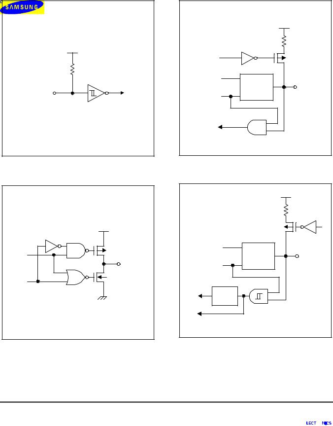
PRODUCT OVERVIEW |
S3C8248/C8245/P8245/C8247/C8249/P8249 |
|
|
PIN CIRCUITS
VDD
In
Figure 1-4. Pin Circuit Type B (RESET)
|
VDD |
Data |
P-Channel |
|
|
|
Out |
Output |
N-Channel |
Disable |
|
Figure 1-5. Pin Circuit Type C
VDD
Pull-up |
|
P-Channel |
|
Enable |
|
||
|
|
||
Data |
Circuit |
|
|
|
I/O |
||
Output |
Type C |
||
|
|||
|
|
||
Disable |
|
|
Figure 1-6. Pin Circuit Type D-2 (P3) |
|||
|
VDD |
|
|
|
VDD |
|
|
Data |
|
Pull-up |
|
Pin Circuit |
Enable |
||
|
I/O |
||
Output |
Type C |
||
|
|||
|
|
||
Disable |
|
|
|
Noise |
|
|
|
Filter |
|
|
|
Ext.INT |
|
|
|
Input |
|
|
|
Normal |
|
|
|
Figure 1-7. Pin Circuit Type D-4 (P0) |
|||
1-8

S3C8248/C8245/P8245/C8247/C8249/P8249 |
|
|
PRODUCT OVERVIEW |
|
|
|
|
|
VDD |
VDD |
|
|
|
|
Open drain |
Pull-up |
|
|
|
Enable |
Pull-up |
|
|
|
VDD |
Resistor |
|
|
|
Enable |
|
|
||
|
|
|
|
|
P-CH |
|
Data |
Circuit |
|
Data |
|
Output |
Type C |
|
|
I/O |
I/O |
||
|
Disable |
|
||
N-CH |
|
ADC & VLD |
|
|
Output |
|
|
|
|
|
Enable |
|
|
|
Disable |
|
|
|
|
|
|
|
|
|
|
|
Data |
|
|
|
|
VLDREF |
|
|
Schmitt Trigger |
|
To ADC |
|
|
|
|
|
|
|
Figure 1-8. Pin Circuit Type E-2 (P1) |
Figure 1-10. Pin Circuit Type F-18 (P2.7/VLDREF) |
|||
|
VDD |
VLC2 |
|
|
|
|
|
Pull-up |
|
VLC1 |
|
Enable |
|
|
|
|
|
|
|
Data |
Circuit |
|
|
Output |
Type C |
SEG/ |
Out |
Disable |
I/O |
||
|
COM |
|
|
|
|
|
|
ADCEN |
|
|
|
|
|
VLC0 |
|
Data |
|
|
|
To ADC |
|
|
|
Figure 1-9. Pin Circuit Type F-10 (P2.0–P2.6) |
Figure 1-11. Pin Circuit Type H (SEG/COM) |
||
1-9
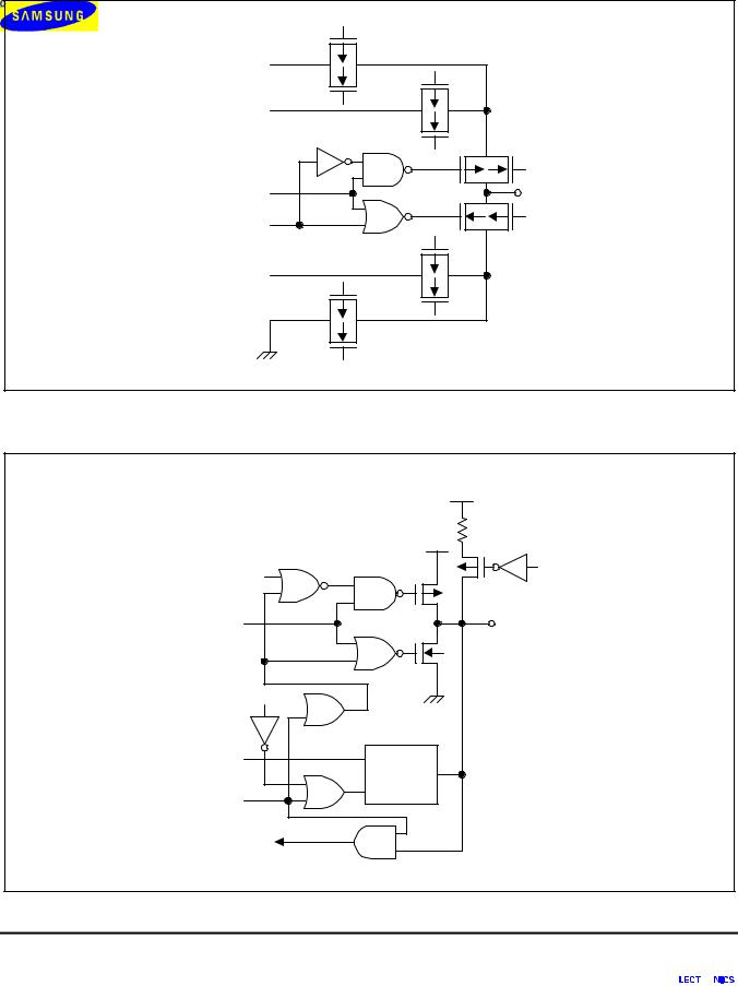
PRODUCT OVERVIEW |
S3C8248/C8245/P8245/C8247/C8249/P8249 |
|
|
VLC2
VLC1
SEG
Output
Disable
VLC0
Figure 1-12. Pin Circuit Type H-4
VDD
VDD
Open Drain EN
Data
LCD Out EN 
SEG |
Output |
Disable |
Pull-up
Enable
Circuit
Type H-4
Figure 1-13. Pin Circuit Type H-14 (P4, P5)
1-10
 Loading...