


S3C8847/C8849/P8849 |
.com |
PRODUCT OVERVIEW |
|
|
1DataSheet4UPRODUCT OVERVIEW
.
wwwSAM87 PRODUCT FAMILY
Samsung'sSAM87 family of 8-bit single-chip CMOS microcontrollers offers a fast and efficient CPU, a wide range of integrated peripherals, and various mask-programmable ROM sizes. Important CPU features include:
— Efficient register-oriented architecture |
|
|
— Selectable CPU clock sources |
. |
|
— Release of Idle and Stop power-down modes by interrupt |
||
— Built-in basic timer circuit with watchdog function |
||
DataSheet4U |
com |
|
A sophisticated interrupt structure recognizes up to eight interrupt levels. Each level can have one or more interrupt sources and vectors. Fast interrupt processing (within a minimum of six CPU clocks) can be assigned to specific interrupt levels.
S3C8847/C8849/P8849 MICROCONTROLLERS
The S3C8847 microcontroller has a 24-Kbyte on-c ip program m mory and the S3C8849 has a 32-Kbyte. Both chips have a 272-byte general-purpose internal register file. The interrupt structure has nine interrupt sources with nine interrupt vectors. The CPU recognizes seven interrupt priority levels.
Using a modular design approach, the following peripherals were integrated with the SAM87 core to make the S3C8847/C8849/P8849 microcontrollers sui ble for use in color television and other types of screen display applications:
— Four programmable I/O ports (26 pins total: 16 general-purpose I/O pins; 10 n-channel, open-drain
|
output pins) |
|
|
— 4-bit resolution A/D converter (4 channels) |
|
||
— |
14-bit PWM output (T |
. |
|
o channels: push-pull type, open-drain type) |
|
||
— |
Basic timer (BT) ith |
atchdog timer function |
|
— One 8-bit timer/counter (T0) with interval timer and PWM mode |
|
||
— One 8-bit general-purpose timer/counter (TA) with prescalers |
|
||
— On-screen display (OSD) with a wide range of programmable features, including halftone control |
|
||
|
signal output |
|
|
|
www |
.com |
|
The S3C8847 and the S3C8849 are available in versatile 42-pin SDIP package. |
|||
OTP |
|
||
The S3C8847/C8849 microcontrollers are also available in OTP (One Time Programmable)DataSheet4Uversion, named the .
S3P8849. The S3P8849 microcontroller has an on-chip 32-Kbyte one-time-programmable EPROM instead of a masked ROM. The KS88P8432 is comparable to the S3C8847/C8849, both in function and pin configuration.
www |
1-1 |
|

PRODUCT OVERVIEW |
S3C8847/C8849/P8849 |
|
|
FEATURES
CPU
•SAM87 CPU core
Memory
•24-Kbyte (S3C8847) or 32-Kbyte (S3C8849) internal program memory
•272-byte general-purpose register area
Instruction Set
•78 instructions
•IDLE and STOP instructions added for powerdown modes
Instruction Execution Time
•750 ns (minimum) with an 8 MHz CPU clock
Interrupts
•9 interrupt sources with 9 vectors
•7 interrupt levels
•Fast interrupt processing for select levels
General I/O
•Four I/O ports (26 pins total)
•Six open-drain pins for up to 6 V loads
•Four open-drain pins for up to 5 V loads
8-Bit Basic Timer
•Three selectable internal clock frequencies
•Watchdog or oscillation stabilization function
Timer/Counters
•One 8-bit timer/counter (T0) with three internal clocks or an external clock and interval timer mode or PWM mode.
•One general-purpose 8-bit timer/counters with interval timer mode (timer A)
A/D Converter
•Four analog input pins; 4-bit resolution
•3.125 µs conversion time (8 MHz CPU clock)
Pulse Width Modulation Module
•14-bit PWM with two-channel output (push-pull type, open-drain type)
•8-bit PWM with four-channel, push-pull and opendrain
•PWM counter and data capture input pin
•Frequency: 5.859 kHz to 23.437 kHz with a 6 MHz CPU clock
On-Screen Display (OSD)
•Video RAM: 252 × 13-bits
•Character generator ROM: 384 × 18 × 16-bits (384 display characters; fixed; 2, variable; 382)
•252 display positions (12 rows × 21 columns)
•16-dot × 18-dot character resolution
•16 different character sizes
•Eight character colors
•Vertical direction fade-in/fade-out control
•Eight colors for character and frame background
•Halftone control signal output; selectable for individual characters
•Synchronous polarity selector for H-sync and V-sync input
Oscillator Frequency
•5 MHz to 8 MHz external crystal oscillator
•Maximum 8 MHz CPU clock
Operating Temperature Range
•– 20°C to + 85°C
Operating Voltage Range
•4.5 V to 5.5 V
Package Type
•42-pin SDIP
1-2

S3C8847/C8849/P8849 |
PRODUCT OVERVIEW |
|
|
BLOCK DIAGRAM
|
|
P0.0 - P0.7 |
|
P1.0 - P1.7 |
|
|
|
RESET |
Port 0 |
|
Port 1 |
|
|
|
INT0 - INT3 |
|
Test |
|
||
|
|
|
|
|
||
XIN |
Main |
|
SAM87 Bus |
|
|
|
XOUT |
Osc |
|
|
|
Timer A |
|
|
|
Port I/O and Interrupt |
|
|
||
|
|
|
|
Control |
|
|
OSCIN |
L-C Osc |
|
|
|
|
TO |
OSCOUT |
|
|
|
|
||
|
|
|
|
Timer 0 |
||
|
|
|
|
|
|
|
H-sync |
|
|
|
|
|
T0CK |
|
|
|
|
|
|
|
V-sync |
|
|
|
|
|
|
Vred |
On- |
|
SAM87 CPU |
PWM |
|
|
Vgreen |
|
|
||||
Screen |
|
|
|
Block |
|
|
Vblue |
|
|
|
|
||
Display |
|
|
|
|
|
|
Vblank |
|
|
|
|
|
|
|
|
|
|
PWM |
|
|
OSDHT |
|
|
|
|
|
|
|
|
|
|
Counter |
|
|
|
|
|
|
|
CAPA |
|
|
|
|
|
|
and Data |
|
|
|
|
|
|
|
|
ADC0 |
|
24/32-KByte |
272-Byte Register |
Capture |
|
|
4-Bit |
|
|
||||
ADC1 |
ROM |
|
File |
|
|
|
ADC2 |
ADC |
|
|
|
14-Bit |
PWM0 |
ADC3 |
|
|
|
|
PWM |
PWM1 |
|
|
|
|
|
|
|
|
|
|
|
SAM87 Bus |
|
|
|
|
|
|
|
8-Bit |
PWM2 |
|
|
|
|
|
PWM3 |
|
|
|
Port 2 |
|
Port 3 |
PWM |
PWM4 |
|
|
|
|
PWM5 |
||
|
|
P2.0 - P2.7 |
|
P3.0 - P3.1 |
|
|
Figure 1-1. Block Diagram
1-3

PRODUCT OVERVIEW |
S3C8847/C8849/P8849 |
|
|
PIN ASSIGNMENTS
|
|
|
|
|
|
|
|
|
|
P0.0 |
P2.5/PWM0 |
|
|
1 |
|
|
|
42 |
|
|
|
|
|
|
|
|
|
|
||||
P2.1/PWM1 |
|
2 |
|
|
|
41 |
|
|
P0.1 |
|
|
|
|
|
|
|
|||||
P2.2/PWM2 |
|
3 |
|
|
|
40 |
|
|
P0.2 |
|
|
|
|
|
|
|
|||||
P2.3/PWM3 |
|
4 |
|
|
|
39 |
|
|
P0.3 |
|
|
|
|
|
|
|
|||||
P2.4/PWM4 |
|
5 |
|
|
|
38 |
|
|
P0.4 |
|
|
|
|
|
|
|
|||||
P2.0/PWM5 |
|
6 |
|
|
|
37 |
|
|
VSS2 |
|
|
|
|
|
|
|
|||||
P2.6/T0 |
|
7 |
|
|
|
36 |
|
|
CAPA |
|
|
|
|
|
|
|
|||||
P1.7/T0CK |
|
8 |
S3C8847/C8849 |
35 |
|
|
P0.5 |
|||
|
|
|
||||||||
P3.0/ADC0 |
|
9 |
34 |
|
|
VDD |
||||
|
|
|
||||||||
P3.1/ADC1 |
|
10 |
42-SDIP |
33 |
|
|
RESET |
|||
|
|
|
||||||||
P0.6/ADC2 |
|
|
11 |
32 |
|
|
XOUT |
|||
|
|
|
|
|
|
|||||
P0.7/ADC3 |
|
12 |
(Top View) |
31 |
|
|
XIN |
|||
|
|
|
||||||||
TEST |
|
13 |
30 |
|
|
VSS1 |
||||
|
|
|
||||||||
P1.0/INT0 |
|
14 |
|
|
|
29 |
|
|
OSCOUT |
|
|
|
|
|
|
|
|||||
P1.1/INT1 |
|
15 |
|
|
|
28 |
|
|
OSCIN |
|
|
|
|
|
|
|
|||||
P1.2/INT2 |
|
16 |
|
|
|
27 |
|
|
V-sync |
|
|
|
|
|
|
|
|||||
P1.3/INT3 |
|
17 |
|
|
|
26 |
|
|
H-sync |
|
|
|
|
|
|
|
|||||
P1.4 |
|
18 |
|
|
|
25 |
|
|
Vblank |
|
|
|
|
|
|
|
|||||
P1.5 |
|
19 |
|
|
|
24 |
|
|
Vred |
|
|
|
|
|
|
|
|||||
P1.6 |
|
20 |
|
|
|
23 |
|
|
Vgreen |
|
|
|
|
|
|
|
|||||
P2.7/OSDHT |
|
21 |
|
|
|
22 |
|
|
Vblue |
|
|
|
|
|
|
|
|||||
|
|
|
|
|
|
|
|
|
|
|
Figure 1-2. S3C8847/C8849/P8849 Pin Assignment Diagram
1-4

S3C8847/C8849/P8849 PRODUCT OVERVIEW
PIN DESCRIPTIONS
Table 1-1. S3C8847/C8849/P8849 Pin Descriptions
|
Pin Name |
Pin |
Pin Description |
Circuit |
Pin |
Share |
|
|
|
Type |
|
Type |
Numbers |
Pins |
|
|
|
|
|
|
|
|
|
|
P0.0–P0.3 |
I/O |
General I/O port (4-bit), configurable for |
2 |
39–42 |
(see pin |
|
|
|
|
digital input or n-channel open-drain, push- |
|
|
description) |
|
|
|
|
pull output. |
|
|
|
|
|
|
|
Pins can withstand up to 5 V loads. |
|
|
|
|
|
|
|
|
|
|
|
|
|
P0.4–P0.5 |
|
General I/O port (2-bit), configurable for |
3 |
38, 35 |
|
|
|
|
|
digital input or push-pull output. |
|
|
|
|
|
|
|
|
|
|
|
|
|
P0.6–P0.7 |
|
General I/O port (2-bit), configurable for |
6 |
11–12 |
ADC2–ADC3 |
|
|
|
|
digital input or n-channel open-drain output. |
|
|
|
|
|
|
|
P0.6–P0.7 can withstand up to 5 V loads. |
|
|
|
|
|
|
|
Multiplexed for alternative use as external |
|
|
|
|
|
|
|
inputs, ADC2–ADC3. |
|
|
|
|
|
|
|
|
|
|
|
|
|
P1.0–P1.3 |
I/O |
General I/O port (4-bit), configurable for |
7 |
14–17 |
INT0–INT3 |
|
|
|
|
digital input or n-channel open-drain output. |
|
|
|
|
|
|
|
P1.0–P1.3 can withstand up to 6 V loads. |
|
|
|
|
|
|
|
Multiplexed for alternative use as external |
|
|
|
|
|
|
|
interrupt inputs, INT0–INT3. |
|
|
|
|
|
|
|
|
|
|
|
|
|
P1.4–P1.5 |
|
General I/O port (2-bit), configurable for |
5 |
18–19 |
|
|
|
|
|
digital input or n-channel open-drain output. |
|
|
|
|
|
|
|
P1.4–P1.5 can withstand up to 6 V loads. |
|
|
|
|
|
|
|
High current port(10mA) |
|
|
|
|
|
|
|
|
|
|
|
|
|
P1.6–P1.7 |
|
General I/O port (2-bit), configurable for |
3 |
20, 8 |
T0CK |
|
|
|
|
digital input or push-pull output. |
|
|
|
|
|
|
|
Each pin has an alternative function. |
|
|
|
|
|
|
|
P1.7: T0CK (Timer 0 clock input) |
|
|
|
|
|
|
|
|
|
|
|
|
|
P2.0–P2.7 |
I/O |
General I/O port (8-bit). Input/output mode |
2 |
1–7, 21 |
PWM0– |
|
|
|
|
or n-channel open-drain, push-pull output |
|
|
PWM5 |
|
|
|
|
mode are software configurable. Pins can |
|
|
T0, OSDHT |
|
|
|
|
withstand up to 5 V loads. |
|
|
|
|
|
|
|
Each pin has an alternative function. |
|
|
|
|
|
|
|
P2.0: PWM5 (8-bit PWM output) |
|
|
|
|
|
|
|
P2.1: PWM1 (14-bit PWM output) |
|
|
|
|
|
|
|
P2.2: PWM2 (8-bit PWM output) |
|
|
|
|
|
|
|
P2.3: PWM3 (8-bit PWM output) |
|
|
|
|
|
|
|
P2.4: PWM4 (8-bit PWM output) |
|
|
|
|
|
|
|
P2.5: PWM0 (14-bit PWM output) |
|
|
|
|
|
|
|
P2.6: T0 (Timer 0 PWM and interval output) |
|
|
|
|
|
|
|
P2.7: OSDHT (Halftone signal output) |
|
|
|
|
|
|
|
|
|
|
|
|
|
P3.0–P3.1 |
I/O |
General I/O port (2-bit), configurable for |
6 |
9–10 |
ADC0–ADC1 |
|
|
|
|
digital input or n-channel open-drain output. |
|
|
|
|
|
|
|
P3.0–P3.1 can withstand up to 5 V loads. |
|
|
|
|
|
|
|
Multiplexed for alternative use as external |
|
|
|
|
|
|
|
inputs ADC0–ADC1. |
|
|
|
|
|
|
|
|
|
|
|
|
|
|
|
|
|
|
|
|
1-5

PRODUCT OVERVIEW |
S3C8847/C8849/P8849 |
|
|
Table 1-1. S3C8847/C8849/P8849 Pin Descriptions (Continued)
Pin Name |
Pin |
Pin Description |
Circuit |
Pin |
Share |
|
Type |
|
Type |
Numbers |
Pins |
PWM0– |
O |
Output pin for 14-bit PWM circuit |
2 |
1, 2 |
P2.5, P2.1 |
PWM1 |
|
|
|
|
|
|
|
|
|
|
|
PWM2– |
O |
Output pin for 8-bit PWM circuit |
2 |
3–6 |
P2.2–P2.4, |
PWM5 |
|
|
|
|
P2.0 |
|
|
|
|
|
|
ADC0–ADC3 |
I |
Analog inputs for 4-bit A/D converter |
6 |
9–12 |
P3.0–P3.1, |
|
|
|
|
|
P0.6–P0.7 |
|
|
|
|
|
|
INT0–INT3 |
I |
External interrupt input pins |
7 |
14–17 |
P1.0–P1.3 |
|
|
|
|
|
|
T0 |
O |
Timer 0 output (interval, PWM) |
2 |
7 |
P2.6 |
|
|
|
|
|
|
T0CK |
I |
Timer 0 clock input |
3 |
8 |
P1.7 |
|
|
|
|
|
|
OSDHT |
O |
Halftone control signal output for OSD |
2 |
21 |
P2.7 |
|
|
|
|
|
|
Vblue, Vgreen |
O |
Digital blue, green, red, and video blank |
4 |
22–25 |
– |
Vred, Vblank |
|
signal outputs for OSD |
|
|
|
|
|
|
|
|
|
H-sync, |
I |
H-sync, V-sync input for OSD |
1 |
26, 27 |
– |
V-sync |
|
|
|
|
|
|
|
|
|
|
|
OSCIN, |
I, O |
L-C oscillator pins for OSD clock frequency |
– |
28, 29 |
– |
OSCOUT |
|
generation |
|
|
|
XIN, XOUT |
I, O |
System clock pins |
– |
31, 32 |
– |
RESET |
I |
System reset input pin |
8 |
33 |
– |
|
|
|
|
|
|
TEST |
– |
Test Pin (must be connected to VSS). |
– |
13 |
– |
|
|
Factory test mode is activated when 12V is |
|
|
|
|
|
applied. |
|
|
|
|
|
|
|
|
|
VDD, VSS1, |
– |
Power supply pins |
– |
34, 30, 37 |
– |
VSS2 |
|
|
|
|
|
CAPA |
I |
Input for capture A module |
1 |
36 |
– |
|
|
|
|
|
|
1-6

S3C8847/C8849/P8849 |
PRODUCT OVERVIEW |
|
|
PIN CIRCUITS
Input |
Noise |
|
Filter |
||
|
Figure 1-3. Pin Circuit Type 1 (V-Sync H-Sync, CAPA)
VDD
Data
I/O
Open-drain

Output
Disable
VSS
Input
Figure 1-4. Pin Circuit Type 2 (P2.0–P2.7, P0.0–P0.3, PWM0–PWM5, T0, OSDHT)
1-7
PRODUCT OVERVIEW |
S3C8847/C8849/P8849 |
|
|
VDD
Data |
I/ O |
|
VSS |
Input |
|
Figure 1-5. Pin Circuit Type 3 (P0.4–P0.5, P1.6–P1.7, T0CK)
VDD
Data |
Output |
VSS
Figure 1-6. Pin Circuit Type 4 (Vblue, Vgreen, Vred, Vblank)
1-8
S3C8847/C8849/P8849 |
PRODUCT OVERVIEW |
|
|
I/O
Data
VSS
Input
NOTE: Circuit type 5 can withstand up to 6 V loads.
Figure 1-7. Pin Circuit Type 5 (P1.4–P1.5)
I/O
Data
VSS
Input
A/D In
NOTE: Circuit type 6 can withstand up to 5 V loads.
Figure 1-8. Pin Circuit Type 6 (P3.0–P3.1, P0.6–P0.7, ADC0–ADC3)
1-9
PRODUCT OVERVIEW |
S3C8847/C8849/P8849 |
|
|
|
I/O |
Data |
|
|
VSS |
Input |
|
INT |
Noise Filter |
NOTE: Circuit type 7 can withstand up to 6 V loads.
Figure 1-9. Pin Circuit Type 7 (P1.0–P1.3, INT0–INT3)
200 KΩ 
Input
Noise
Filter
Figure 1-10. Pin Circuit Type 8 (RESET)
1-10
S3C8847/C8849/P8849 |
ADDRESS SPACES |
|
|
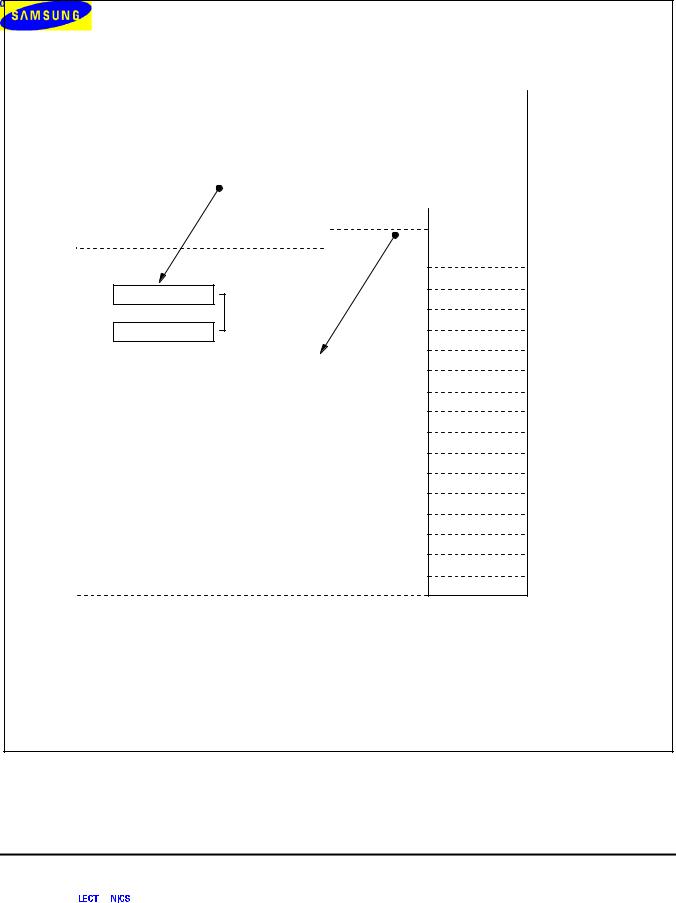
2 ADDRESS SPACES
OVERVIEW
The S3C8847 and S3C8849 microcontrollers have two kinds of address space:
—Internal program memory (ROM)
—Internal register file
The S3C8847 has an on-chip 24-Kbyte mask-programmable ROM; the S3C8849 has a 32-Kbyte. An external memory interface is not implemented.
There are 272 general-purpose 8-bit data registers in the register file. Thirteen 8-bit registers are used for CPU and system control. To support peripheral, I/O, and clock functions, there are 20 control registers and 9 data registers. In addition, there is a 252 × 13-bit area for on-screen display (OSD) video RAM.
2-1

ADDRESS SPACES |
S3C8847/C8849/P8849 |
|
|
PROGRAM MEMORY (ROM)
Program memory (ROM) stores program codes or table data. The S3C8847 has a 24-Kbyte mask-programmable program memory (5FFFH) and the S3C8849 has a 32-Kbyte (7FFFH).
As shown in Figure 2-1, the first 256 bytes of the ROM (0H–0FFH) are reserved for interrupt vector addresses. Unused locations in this range can be used as normal program memory. If the vector address area is used to store normal program data, care must be taken to avoid overwriting vector addresses stored in these locations. The ROM address at which program execution starts after a RESET is 0100H.
(Decimal) |
|
|
(Hex) |
(Decimal) |
|
|
(Hex) |
||||||||
65,535 |
|
|
|
|
|
FFFFH |
65,535 |
|
|
|
|
|
FFFFH |
||
|
|
|
|
|
|
|
|
||||||||
|
|
|
|
|
|
|
|
|
|
|
|
|
|
|
|
|
~ |
|
Not Used |
~ |
|
|
~ |
|
Not Used |
~ |
|
||||
|
|
|
|
|
|
|
|
|
|
|
|
|
|
|
|
|
|
|
|
|
|
B6FFH |
|
|
|
|
|
|
B600H |
||
46,591 |
|
|
|
|
B5FFH |
46,591 |
|
|
|
|
|
B5FFH |
|||
|
|
|
|
OSD FONT ROM |
|
|
|
|
|
|
|
OSD FONT ROM |
|
|
|
|
|
|
|
|
|
8000H |
|
|
|
|
|
|
8000H |
||
32,767 |
|
|
|
|
|
7FFFH |
32,767 |
|
|
|
|
|
7FFFH |
||
|
|
|
|
Not Used |
|
|
|
|
|
|
|
|
|
|
|
|
|
|
|
|
|
6000H |
|
|
|
|
32-KB |
|
|
|
|
24,575 |
|
|
|
|
|
5FFFH |
|
|
|
|
|
|
|
||
|
|
|
24-KB |
|
|
|
|
|
Program |
|
|
|
|||
|
|
|
|
|
|
|
|
|
|
|
Memory Area |
|
|
|
|
|
|
|
|
Program |
|
|
|
|
|
|
|
|
|
|
|
|
|
|
|
|
|
|
|
|
|
|
|
|
|
|
|
|
|
|
|
Memory Area |
|
|
|
|
|
|
|
|
|
|
|
255 |
|
|
|
Interrupt |
|
0FFH |
255 |
|
|
|
Interrupt |
|
0FFH |
||
|
|
|
|
|
|
|
|
|
|
|
|
|
|
||
0 |
|
|
Vector Area |
|
0H |
0 |
|
|
Vector Area |
|
0H |
||||
|
|
|
|
|
|
|
|
||||||||
|
|
|
|
S3C8847 |
|
|
|
|
|
|
|
S3C8849/P8849 |
|
|
|
Figure 2-1. Program Memory Address Spaces
2-2

S3C8847/C8849/P8849 |
ADDRESS SPACES |
|
|
REGISTER ARCHITECTURE
The upper 64 bytes of the S3C8847/C8849/P8849 internal register file is logically expanded into two 64-byte areas, called set 1 and set 2. The upper 32-byte area of set 1 is divided into two register banks, called bank 0 and bank 1. In addition, two register pages are implemented, called page 0 and page 1. The total addressable register space is thereby expanded from 256 bytes to 569 bytes.
The extension of the physical register space into separately addressable areas (sets, banks, and pages) is supported by various addressing mode restrictions, the select bank instructions, SB0 and SB1, and the register page pointer (PP).
Specific register types and the area (in bytes) that they occupy in the register file are summarized in Table 2-1.
Table 2-1. Register Type Summary
Register Type |
Number of Bytes |
|
|
General-purpose registers (including the 16-byte |
272 |
working register common area) |
|
CPU and system control registers |
16 |
Peripheral, I/O, and clock control/data registers |
29 |
On-screen display (OSD) video RAM |
252 |
|
|
Total Addressable Bytes |
569 |
|
|
2-3

ADDRESS SPACES |
S3C8847/C8849/P8849 |
|
|
|
|
|
|
|
|
|
|
|
|
|
|
|
|
|
|
|
|
|
|
SET 1 |
|
|
|
|
|
|
|
|
|
PAGE 0 |
|
|
|
|
|
|
PAGE 1 |
||||
|
|
|
|
|
|
|
|
|
|
|
|
|
|
|
|
|
|
|
|
|
|
|
FFH |
FFH |
|
|
|
|
|
FFH |
|
|
|
|
|
|
|||||
|
|
|
|
|
|
|
|
|
|
|
|
|
|
|
|
|
|
|
|
BANK 1 |
|
|
|
|
|
NOT USED |
|
|
|
|
|||||||||||
|
|
|
|
|
|
|
|
|
|
|
|
|
|
|
|
|
|
|
|
|
|
|
|
|
|
|
|
|
|
|
|
|
FC H |
|
|
|
|
|
|||
|
|
|
|
|
|
|
FFH |
|
|
|
|
|
|
|
|
|
|
|
|
|
|
|
|
|
|
|
|
|
|
|
|
|
|||||||||
|
|
|
|
|
|
|
|
|
|
|
|
|
|
|
|
|
|
|
|
|
|
|
|
|
|
|
|
|
|
|
|||||||||||
|
|
|
|
|
|
|
|
|
|
|
|
BANK 0 |
|
|
|
|
|
|
|
|
|
|
|
|
|
FBH |
|
|
|
|
|
|
|||||||||
|
|
|
|
|
|
|
|
|
|
|
|
|
|
|
|
|
|
|
|
|
|
|
|
|
|
|
|
|
|
|
|
|
|
|
|
|
|
|
|||
|
|
|
|
|
32 |
|
|
|
|
|
|
|
|
|
|
SYSTEM AND |
|
|
|
|
|
|
|
|
|
SET 2 |
|
|
|
|
|
|
SET 2 |
|
|
|
|
||||
|
|
|
|
BYTES |
|
|
|
|
|
|
|
|
|
|
|
|
|
|
|
|
|
|
|
|
|
|
|
||||||||||||||
|
|
|
|
|
|
|
|
|
|
|
|
|
|
|
|
|
|
|
PERIPHERAL |
|
|
|
|
|
|
|
|
|
|
|
|
|
|
|
|
|
|
|
|
|
|
|
|
|
|
|
|
|
|
|
|
|
|
|
|
|
|
|
|
|
|
CONTROL |
|
|
E0H |
|
|
|
|
GENERAL- |
|
|
|
|
|
|
OSD REGISTER FILE |
|
|
|
|
||
|
|
|
|
|
|
|
|
|
|
|
|
|
|
|
|
|
|
|
|
REGISTERS |
|
|
|
|
|
|
|
|
|
|
|
|
|
|
|
|
|||||
|
|
|
|
|
|
|
|
|
|
|
|
|
|
|
|
|
|
|
|
|
|
|
|
|
|
|
|
|
|
|
|
|
|
|
(VIDEO RAM, |
|
|
|
|
||
|
64 |
|
|
|
E0H |
|
|
|
|
|
|
|
|
|
|
|
|
|
|
|
PURPOSE DATA |
|
|
|
|
|
|
INDIRECT |
|
|
|
|
|||||||||
|
BYTES |
|
DFH |
|
|
|
|
|
|
|
|
|
|
|
|
|
|
|
REGISTERS |
|
|
|
|
|
|
|
|
|
|
||||||||||||
|
|
|
|
|
|
|
SYSTEM |
|
|
|
|
|
|
|
|
|
|
|
|
|
|
|
ADDRESSING ONLY) |
|
|
|
|
||||||||||||||
|
|
|
|
|
|
|
|
|
|
|
|
|
|
|
|
|
|
|
|
|
|
|
|
|
|
|
|
|
|
|
|
|
|
|
|
|
|
|
|
||
|
|
|
|
|
|
D0H |
|
|
|
|
|
REGISTERS |
|
|
|
|
|
|
|
|
|
|
|
|
|
|
|
|
|
|
|
|
|
||||||||
|
|
|
|
|
|
|
|
|
|
|
|
|
|
|
|
|
|
|
|
|
|
|
|
|
|
|
|
|
|
|
|
|
|||||||||
|
|
|
|
|
|
CFH |
|
|
|
|
|
|
|
|
|
|
|
C0H |
|
|
|
|
|
C0H |
|
|
|
|
|
|
|||||||||||
|
|
|
|
|
|
|
|
|
|
|
WORKING |
|
|
|
|
|
|
|
|
|
|
|
|
|
256 |
||||||||||||||||
|
|
|
|
|
|
|
|
|
|
|
|
|
|
|
|
|
|
|
|
|
|
|
|
|
|
|
|
|
|
|
|
|
|||||||||
|
|
|
|
|
|
C0H |
|
|
|
|
|
REGISTERS |
|
|
|
|
|
BFH |
|
|
|
|
|
BFH |
|
|
|
BYTES |
|||||||||||||
|
|
|
|
|
|
|
|
|
|
|
|
|
|
|
|
|
|
|
|
|
PRIME DATA |
|
|
|
|
|
|
OSD REGISTER FILE |
|
|
|
|
|||||||||
|
|
|
|
|
|
|
|
|
|
|
|
|
|
|
|
|
|
|
|
|
|
|
|
|
|
|
|
|
|
|
|||||||||||
|
|
|
|
|
|
|
|
|
|
|
|
|
|
|
|
|
|
|
|
|
|
|
|
|
|
|
|
|
|
|
|
|
|
|
|
|
|
|
|
||
|
|
|
|
|
|
|
|
|
|
|
|
|
|
|
|
|
|
|
|
|
|
|
192 |
|
|
|
|
|
|
|
|
|
|
||||||||
|
|
|
|
|
|
|
|
|
|
|
|
|
|
|
|
|
|
|
|
|
|
|
|
~ |
REGISTERS |
~ |
|
|
~ |
(VIDEO RAM, ALL |
~ |
|
|
|
|||||||
|
|
|
|
|
|
|
|
|
|
|
|
|
|
|
|
|
|
|
|
|
|
|
BYTES |
|
|
|
|
|
|
||||||||||||
|
|
|
|
|
|
|
|
|
|
|
|
|
|
|
|
|
|
|
|
|
|
|
|
|
|
(ALL ADDRESSING |
|
|
|
|
|
|
ADDRESSING |
|
|
|
|
||||
|
|
|
|
|
|
|
|
|
|
|
|
|
|
|
|
|
|
|
|
|
|
|
|
|
|
|
|
|
|
|
|
|
|
|
|
|
|
|
|
||
|
|
|
|
|
|
|
|
|
|
|
|
|
|
|
|
|
|
|
|
|
|
|
|
|
|
|
|
|
|
MODES) |
|
|
|
|
|
|
MODES) |
|
|
|
|
|
|
|
|
|
|
|
|
|
|
|
|
|
|
|
|
|
|
|
|
|
|
|
|
|
|
00H |
|
|
|
|
|
00H |
|
|
|
|
|
|
|||
|
|
|
|
|
|
|
|
|
|
|
|
|
|
|
|
|
|
|
|
|
|
|
|
|
|
|
|
|
|
|
|
|
|
|
|
||||||
|
|
|
|
|
|
|
|
|
|
|
|
|
|
|
|
|
|
|
|
|
|
|
|
|
|
|
|
|
|
|
|
|
|
|
|
|
|
|
|
|
|
Figure 2-2. Internal Register File Organization
2-4

S3C8847/C8849/P8849 |
ADDRESS SPACES |
|
|
REGISTER PAGE POINTER (PP)
The SAM87 architecture supports the logical expansion of the physical 256-byte register file in up to 16 separately addressable register pages. Page addressing is controlled by the register page pointer, PP, DFH. Only two pages are implemented in the S3C8847/C8849/P8849 microcontrollers: page 0 is used as general-purpose register space and page 1 contains a 252 × 13-bit area for the on-screen display (OSD) video ROM.
As shown in Figure 2-3, when the upper nibble of the PP register is '0000B', the selected destination address is located on page 0. When the upper nibble value is '0001B', page 1 is the selected destination. The lower nibble of the page pointer controls the source register page destination addressing: when the lower nibble is '0000B', page 0 is the selected source register page; when the lower nibble is '0001B', page 1 is the source register page.
After a reset, the page pointer's source valuethe( lower nibble) and the destination value (the upper nibble) are always '0000B', automatically selecting page 0 as bothe source and the destination. To select page 1 as the source or destination register page, you must modify the register page pointer values accordingly. Because only page 0 and page 1 are used in the S3C8847/C8849/P8849 implementation, only pointer values '0000B' and '0001B' are used.
REGISTER PAGE POINTER (PP)
DFH, Set 1, R/W
|
|
|
MSB |
.7 |
.6 |
|
.5 |
.4 |
|
|
.3 |
|
|
.2 |
|
.1 |
.0 |
|
LSB |
||||
|
|
|
|
|
|
|
|
|
|
|
|
|
|
|
|
|
|
||||||
|
|
|
|
|
|
|
|
|
|
|
|
|
|
|
|
|
|
|
|
|
|
|
|
|
|
|
|
|
|
|
|
|
|
|
|
|
|
|
|
|
|
|
|
|
|
|
|
Destination register page selection bits: |
|
|
|
|
|
Source register page selection bits: |
|||||||||||||||||
|
|
|
|
|
|
|
|
|
|
|
|
|
|
|
|
||||||||
0 |
0 |
0 |
0 B |
|
Destination: page 0 |
|
|
|
0 |
0 |
0 |
0 B |
|
Source: page 0 |
|
||||||||
0 |
0 |
0 |
1 B |
|
Destination: page 1 |
|
|
|
0 |
0 |
0 |
1 B |
|
Source: page 1 |
|
||||||||
|
|
. |
|
|
Not used for the |
|
|
|
|
|
|
|
|
. |
|
|
Not used for the |
|
|||||
|
|
. |
|
|
S3C8847/C8849/P8849 |
|
|
|
|
|
|
|
. |
|
|
S3C8847/C8849/P8849 |
|||||||
|
|
. |
|
|
|
|
. |
|
|
|
|
|
|
|
|
|
. |
|
|
|
. |
|
|
|
|
|
|
|
|
|
. |
|
|
|
|
|
|
|
|
|
|
|
|
|
. |
|
|
1 |
1 |
1 |
1 B |
|
Not used for the |
|
|
|
1 |
1 |
1 |
1 B |
|
Not used for the |
|
||||||||
|
|
|
|
|
S3C8847/C8849/P8849 |
|
|
|
|
|
|
|
|
|
|
S3C8847/C8849/P8849 |
|||||||
|
|
|
|
|
|
|
|
|
|
|
|
|
|
|
|||||||||
Figure 2-3. Register Page Pointer (PP)
2-5
ADDRESS SPACES |
S3C8847/C8849/P8849 |
|
|
+ PROGRAMMING TIP – Data Operations Between Register Pages
LD |
PP,#10H |
; |
Destination register page 1, source register page 0 |
|
LD |
20H,45H |
; |
Register 20H in page 1 |
← Content of the register 45H |
|
|
; |
in page 0 |
|
• |
|
|
|
|
• |
|
|
|
|
• |
|
|
|
|
ADD |
30H,40H |
; |
Register 30H in page 1 |
← Content of 30H in page 1 |
|
|
; plus (+) the content of 40H in page 0 |
||
 +
+
45H
40H
30H
20H
PAGE 0 |
PAGE 1 |
Figure 2-4. Programming Tip Example for Inter-Page Data Operations
EFFECT OF DIFFERENT INSTRUCTIONS FOR INTER-PAGE DATA OPERATIONS
The source and the destination pages for data operations between pages differ, depending on which instruction you use. The following programming tip, "Examples of Inter-Page Data Transfer Operations," provides you with a detailed list of various case.
2-6

S3C8847/C8849/P8849 |
ADDRESS SPACES |
|
|
+ PROGRAMMING TIP – Examples of Inter-Page Data Transfer Operations
Example 1. |
a) |
ADC |
R1,R0 |
; R0 – source page |
|
|
|
|
; R1 – destination page |
|
b) |
ADC |
R4,@R2 |
; R2, 40H – source page |
|
|
|
R2 contains 40H |
; R4 – destination page |
|
c) |
ADC |
R0,#0AAH |
; R0 – destination page |
|
d) |
ADC |
40H,42H |
; 42H – source page |
|
|
|
|
; 40H – destination page |
|
e) |
ADC |
40H,@42H |
; 42H, 60H – source page |
|
|
|
42H contains 60H |
; 40H – destination page |
|
f) |
ADC |
40H,#02H |
; 40H – destination page |
NOTE: The above examples also apply to the instructions ADD, SUB, AND, OR, and XOR.
Example 2. |
a) |
BAND |
R0,40H.7 |
; 40H – source page |
||
|
|
|
|
; R0 |
– destination page |
|
|
b) |
BAND |
40H.7,R0 |
; |
R0 |
– source page |
|
|
|
|
; |
40H – destination page |
|
NOTE: The above examples also apply to the instructions BOR, BXOR, and LDB.
Example 3. |
a) |
BCP |
R3,44H.7 |
; 44H – source page |
|
|
|
|
|
; |
R3 – destination page |
Example 4. |
a) |
BITC |
R3.7 |
; |
R3 – destination page |
NOTE: The above examples also apply to the instructions BITR and BITS.
2-7

ADDRESS SPACES |
S3C8847/C8849/P8849 |
|
|
+ PROGRAMMING TIP – Examples of Inter-Page Data Transfer Operations (continued)
Example 5. |
a) BTJRF |
SKIP,R6.7 |
; R6 – source page |
NOTE: The above example also applies to the instructions BTJRT.
Example 6. |
a) |
CALL |
@60H |
; 60H, 61H – source page |
|
Example 7. |
a) |
CLR |
30H |
; 30H – destination page |
|
|
b) |
CLR |
@44H |
; |
44H – source page |
|
|
|
44H contains 40H |
; |
40H – destination page |
NOTE: The above examples also apply to the instructions RL, RLC, and SRA.
Example 8. a) |
COM |
03H |
; 03H – destination page |
|
b) |
COM |
@44H |
; |
44H – source page |
|
|
44H contains 40H |
; |
40H – destination page |
NOTE: The above examples also apply to the instructions DEC, INC, RR, and RRC.
Example 9. |
a) |
CP |
R1,R0 |
; R0 – source page |
|
|
|
|
; R1 – destination page |
|
b) |
CP |
R2,@R4 |
; R4, 40H – source page |
|
|
|
R4 contains 40H |
; R2 – destination page |
|
c) |
CP |
40H,42H |
; 42H – source page |
|
|
|
|
; 40H – destination page |
|
d) |
CP |
40H,@42H |
; 42H, 44H – source page |
|
|
|
42H contains 44H |
; 40H – destination page |
|
e) |
CP |
20H,#0AAH |
; 20H – destination page |
NOTE: The above examples also apply to the instructions TCM and TM.
2-8

S3C8847/C8849/P8849 |
ADDRESS SPACES |
|
|
+ PROGRAMMING TIP – Examples of Inter-Page Data Transfer Operations (Continued)
Example 10. a) CPIJE |
R3,@R5,SKIP |
; |
R5, 40H – source page |
|
R5 contains 40H |
; |
R3 – destination page |
NOTE: The above example also applies to the instruction CPIJNE.
Example 11. |
a) |
DA |
00H |
; 00H – source page |
|
b) |
DA |
@02H |
; 02H – source page |
|
|
|
02H contains 40H |
; 40H – destination page |
Example 12. |
a) |
DECW |
60H |
; 60H, 61H – destination page |
|
b) |
DECW |
@00H |
; 00H, 01H – source page |
|
|
|
00H contains 48H |
; 48H, 49H – destination page |
|
|
|
01H contains 49H |
|
NOTE: The above example also applies to the instruction INCW. |
||||
Example 13. |
a) |
DIV |
60H,40H |
; 40H – source page |
|
|
|
|
; 60H, 61H – destination page |
|
b) |
DIV |
60H,@20H |
; 20H, 40H – source page |
|
|
|
20H contains 40H |
; 60H, 61H – destination page |
|
c) |
DIV |
60H,#03H |
; 60H, 61H – destination page |
NOTE: The above example also applies to the instruction INCW.
Example 14. a) DJNZ |
R6,LOOP |
; R6 – destination page |
NOTE: Incase PP = 10H, 11H, this instruction is not valid.
Example 15. a) JP |
@60H |
; 60H, 61H – source page |
2-9

ADDRESS SPACES |
S3C8847/C8849/P8849 |
|
|
+ PROGRAMMING TIP – Examples of Inter-Page Data Transfer Operations (Continued)
Example 16. a) |
LD |
R0,#0AAH |
; R0 – destination page |
b) |
LD |
R0,40H |
; 40H – source page |
|
|
|
; R0 – destination page |
c) |
LD |
40H,R0 |
; R0 – source page |
|
|
|
; 40H – destination page |
d) |
LD |
R0,@R2 |
; R2, 50H – source page |
|
|
R2 contains 50H |
; R0 – destination page |
e) |
LD |
@R4,R2 |
; R4, R2 – source page |
|
|
R4 contains 40H |
; 40H – destination page |
f) |
LD |
40H,41H |
; 41H – source page |
|
|
|
; 40H – destination page |
g) |
LD |
40H,@42H |
; 42H, 44H – source page |
|
|
42H contains 44H |
; 40H – destination page |
h) |
LD |
45H,#02H |
; 45H – destination page |
i) |
LD |
@40H,#02H |
; 40H – source page |
|
|
40H contains 44H |
; 44H – destination page |
j) |
LD |
@40H,42H |
; 40H, 42H – source page |
|
|
40H contains 44H |
; 44H – destination page |
k) |
LD |
R5,#04H(R0) |
; R0, 04H(2 + offset) – source page |
|
|
R0 contains 02H |
; R5 – destination page |
l) |
LD |
#04H(R0),R1 |
; R0, R1 – source page |
|
|
R0 contains 02H |
; 04H – destination page |
2-10
S3C8847/C8849/P8849 |
ADDRESS SPACES |
|
|
+ PROGRAMMING TIP – Examples of Inter-Page Data Transfer Operations (Continued)
Example 17. |
a) |
LDC |
R0,@RR6 |
; R6, R7 – source page |
|
|
|
|
; R0 – destination page |
|
b) |
LDC |
@RR6,R2 |
; R6, R7, R2 – source page |
|
|
|
RR6 contains an external memory address |
|
|
c) |
LDC |
R0,#01H(RR6) |
; R6, R7 – source page |
|
|
|
|
; R0 – destination page |
|
d) |
LDC |
#01H(RR6),R0 |
; R0, R6, R7 – source page |
|
e) |
LDC |
R0,#1000H(RR6) |
; R6, R7 – source page |
|
|
|
|
; R0 – destination page |
|
f) |
LDC |
#1000H(RR6),R0 |
; R0, R6, R7 – source page |
Example 18. |
a) |
LDCD |
R0,@RR6 |
; R6, R7 – source page |
|
|
|
|
; R0 – destination page |
|
b) |
LDCPD |
@RR6,R0 |
; R0, R6, R7 – source page |
NOTE: The above examples also apply to the instructions LDCI and LDCPI.
Example 19. a) |
LDW |
40H,20H |
; |
20H, 21H |
– source page |
|
|
|
; |
40H, 41H |
– destination page |
b) |
LDW |
60H,@20H |
; |
20H, 40H |
– source page |
|
|
20H contains 40H |
; 60H, 61H – destination page |
||
c) |
LDW |
40H,#02H |
; 40H, 41H – destination page |
||
2-11

ADDRESS SPACES |
S3C8847/C8849/P8849 |
|
|
+ PROGRAMMING TIP – Examples of Inter-Page Data Transfer Operations (Concluded)
Example 20. |
a) |
MULT |
40H,20H |
; 20H – source page |
|
|
|
|
; 40H, 41H – destination page |
|
b) |
MULT |
60H,@20H |
; 20H, 40H – source page |
|
|
|
20H contains 40H |
; 60H, 61H – destination page |
|
c) |
MULT |
40H,#02H |
; 40H, 41H – destination page |
Example 21. |
a) |
POP |
00H |
; 00H – destination page |
|
b) |
POP |
@20H |
; 20H – source page |
|
|
|
20H contains 40H |
; 40H – destination page |
Example 22. |
a) |
POPUD |
00H,@20H |
; 20H, 40H – source page |
|
|
|
20H contains 40H |
; 00H – destination page |
NOTE: The above example also applies to the instruction POPUI.
Example 23. |
a) |
PUSH |
00H |
; 00H – destination page |
|
|
b) |
PUSH |
@20H |
; 20H, 40H – source page |
|
|
|
|
20H contains 40H |
|
|
Example 24. |
a) |
PUSHUD |
@60H,20H |
; |
60H, 20H – source page |
|
|
|
60H contains 44H |
; |
44H – destination page |
NOTE: The above example also applies to the instruction PUSHUI.
Example 25. a) |
SWAP |
00H |
; 00H – destination page |
|
b) |
SWAP |
@20H |
; |
20H – source page |
|
|
20H contains 40H |
; |
40H – destination page |
2-12

S3C8847/C8849/P8849 |
ADDRESS SPACES |
|
|
REGISTER SET 1
The term set 1 refers to the upper 64 bytes of the register file, locations C0H–FFH. This area can be accessed at any time, regardless of which page is currently selected. The upper 32-byte area of this 64-byte space is divided into two 32-byte register banks, called bank 0 and bank 1. You use the select register bank instructions, SB0 or SB1, to address one bank or the other. A reset operation automatically selects bank 0 addressing.
The lower 32-byte area of set 1 is not banked. This area contains 16 bytes for mapped system registers (D0H– DFH) and a 16-byte common area (C0H–CFH) for working register addressing.
Registers in set 1 are directly accessible at all times using Register addressing mode. The 16-byte working register area ,however, can only be accessed using working register addressing. Working register addressing is a function of Register addressing mode (see Chapter 3, "Addressing Modes," for more information).
REGISTER SET 2
The same 64-byte physical space that is used for the set 1 register locations C0H–FFH is logically duplicated to add another 64 bytes. This expanded area of the register file is called set 2. The logical division of set 1 and set 2 is maintained by means of addressing mode restrictions: while you can access set 1 using Register addressing mode only, you should use Register Indirect addressing mode or Indexed addressing mode to access set 2.
For the S3C8847/C8849/P8849, the set 2 address range (C0H–FFH) is accessible on page 0 and page 1. Please note, however, that on page 1, the set 2 locations FCH–FFH are not mapped.
Part of the OSD video RAM is in page 1, set 2 (C0H–FBH), and the other part (00H–BFH) is in the page 1 prime register area. To avoid programming errors, we recommend using either Register Indirect or Indexed mode to address the entire 252-byte video RAM area.
PRIME REGISTER SPACE
The lower 192 bytes (00H–BFH) of the S3C8847/C8849/P8849's two 256-byte register pages is called prime register area. Prime registers can be accessed using any of the seven addressing modes. The prime register area on page 0 is immediately addressable after a reset. In order to address registers on page 1 (in the OSD video RAM), you must first set the register page pointer (PP) to the appropriate source and destination values.
2-13

ADDRESS SPACES |
S3C8847/C8849/P8849 |
|
|
|
|
SET 1 |
|
|
|
|
|
|
|
|
|
|
|
|
|
BANK 0 BANK 1 |
|
|
PAGE 0 |
|
|
PAGE 1 |
|||||
FFH |
|
|
FFH |
|
|
|
|
FFH |
|
|
|
|
|
|
|
|
|
|
|
|
|
|
|
||||
FCH |
|
|
|
|
|
|
|
FBH |
|
|
|
|
|
|
|
|
|
|
|
|
|
|
|
|
|||
|
|
|
|
|
|
|
|
|
|
|
|
|
|
|
|
|
|
|
|
|
|
|
|
|
|
|
|
E0H |
|
|
|
|
|
SET 2 |
|
|
|
|
|
|
|
|
|
|
|
|
|
|
|
|
|
SET 2 |
|
||
|
|
|
|
|
|
|
|
|
|
|
|
|
|
D0H |
|
|
|
|
|
|
|
|
|
|
|
|
|
|
|
|
|
|
|
|
|
|
|
|
|
||
C0H |
|
|
C0H |
|
|
|
|
C0H |
|
|
|
|
|
|
|
|
|
|
|
|
|
|
|
||||
CPU and system control |
|
|
|
|
|
|
|
|
|||||
|
|
|
|
|
|
|
|
|
|
|
|
||
|
|
|
|
|
|
|
|
|
|
|
|
||
|
|
General-purpose |
|
|
|
|
|
|
|
|
|
|
|
|
|
|
|
|
|
|
|
|
|
|
|
||
|
|
|
|
|
|
|
|
|
|
|
|
||
|
|
|
|
|
PRIME |
|
|
|
|
PRIME |
|
||
|
|
|
|
|
|
|
|
|
|
|
|
||
|
|
Peripherals and I/O |
|
|
|
AREA |
|
|
|
|
AREA |
|
|
|
|
|
|
|
|
|
|
|
|
|
|
||
|
|
OSD Video RAM |
|
|
|
|
|
|
|
|
|
|
|
|
|
|
|
|
|
|
|
|
|
|
|
||
|
|
|
|
|
|
|
|
|
|
|
|
||
|
|
Area not mapped |
|
|
|
|
|
|
|
|
|
|
|
|
|
|
|
|
|
|
|
|
|
|
|
||
|
|
|
|
00H |
|
|
|
|
00H |
|
|
|
|
|
|
|
|
|
|
|
|
||||||
|
|
|
|
|
|
|
|
|
|
|
|
||
Figure 2-5. Set 1, Set 2, and Prime Area Register Map
2-14
S3C8847/C8849/P8849 |
ADDRESS SPACES |
|
|
WORKING REGISTERS
Instructions can access specific 8-bit registers or 16-bit register pairs using either 4-bit or 8-bit address fields. When 4-bit working register addressing is used, the 256-byte register file is viewed as thirty two 8-byte register groups or "slices." Each slice consists of eight 8-bit registers. When the two 8-bit register pointers, RP1 and RP0, are used, two working register slices can be selected at any time to form a 16-byte working register block. Using the register pointers, you can move this 16-byte register block anywhere in the addressable register file (except for the set 2 area).
The terms slice and block are used in this manual to help you visualize the size and relative locations of selected working register spaces:
—One working register slice is 8 bytes (eight 8-bit working registers; R0–R7 or R8–R15)
—One working register block is 16 bytes (sixteen 8-bit working registers; R0–R15)
All the registers in an 8-byte working register slice have the same binary value for their five most significant address bits. This makes it possible for each register pointer to point to one of the 24 slices in the register file. The base addresses for the two selected 8-byte register slices are contained in the register pointers, RP0 and RP1. After a reset, RP0 and RP1 always point to the 16-byte common area in set 1 (C0H–CFH).
|
|
|
|
|
Slice 32 |
|
|
FFH |
|
|
|
|
|
|
|
|
F8H |
||
|
|
|
|
|
|
|
|
|
|
1 1 1 1 1 |
X X X |
|
|
|
|
|
|
|
F7H |
|
|
|
|
|
|
|
F0H |
||
|
|
|
|
|
|
|
|
|
|
|
|
|
|
|
|
|
|
|
|
RP1 (Registers R8–R15) |
|
|
|
|
|
|
|
||
Each register pointer points to |
|
|
|
|
|
|
CFH |
||
|
|
|
|
|
|
||||
|
|
|
|
|
|
C0H |
|||
one 8-byte slice of the register |
|
|
|
|
|
|
|||
|
|
|
|
|
|
|
|||
space, selecting a 16-byte |
|
|
|
|
|
|
|
||
working register |
block in total . |
~ |
|
|
~ |
|
|||
|
|
|
|||||||
|
|
|
|||||||
|
|
|
|
|
|
||||
|
|
|
|
|
|||||
Set 1
Only
|
|
|
10H |
0 0 0 0 0 X X X |
|
|
FH |
|
|
8H |
|
|
|
|
|
RP0 (Registers R0–R7) |
|
Slice 1 |
7H |
|
0H |
||
|
|
Figure 2-6. 8-Byte Working Register Areas (Slices)
2-15

ADDRESS SPACES |
S3C8847/C8849/P8849 |
|
|
USING THE REGISTER POINTERS
The register pointers, RP0 and RP1, are mapped to the addresses D6H and D7H in set 1. They are used to select two movable 8-byte working register slices in the register file. After a reset, they point to the working register common area: RP0 points to the addresses C0H–C7H, and RP1 points to the addresses C8H–CFH. If you want to change a register pointer value, you should load a new value to RP0 and/or RP1 using an SRP or LD instruction (see Figures 2-7 and 2-8).
With working register addressing, you can only access those locations that are pointed to by the register pointers. Please note that you cannot use the register pointers to select the working register area in set 2, C0H–FFH, because these locations are accessible only using the Indirect Register or Indexed addressing mode.
The selected 16-byte working register block usually consists of two contiguous 8-byte slices. As a general programming guideline, we recommend that RP0 point to the "lower" slice and RP1 point to the "upper" slice (see Figure 2-7). In some cases, it may be necessary to define working register areas in different (non-contiguous) areas of the register file. In Figure 2-8, RP0 points to the "upper" slice and RP1 to the "lower" slice.
Because a register pointer can point to either of the two 8-byte slices in the working register block, you can flexibly define the working register area.
+ PROGRAMMING TIP — Setting the Register Pointers
SRP |
#70H |
; |
RP0 ← 70H, RP1 ← 78H |
SRP1 |
#48H |
; |
RP0 ← no change, RP1 ← 48H |
SRP0 |
#0A0H |
; |
RP0 ← A0H, RP1 ← no change |
CLR |
RP0 |
; |
RP0 ← 00H, RP1 ← no change |
LD |
RP1,#0F8H |
; |
RP0 ← no change, RP1 ← 0F8H |
0 |
0 |
0 |
0 |
1 |
x |
x |
x |
|
|
|
|
|
|
|
|
|
|
|
|
RP1 |
|
|
|
|
|
|
|
|
|
|
|
0 |
0 |
0 |
0 |
0 |
x |
x |
x |
|
|
|
|
|
|
|
|
|
|
|
|
RP0 |
|
|
|
REGISTER FILE |
|
|
|
CONTAINS 32 |
|
|
|
8-BYTE SLICES |
|
|
|
FH (R15) |
16-BYTE |
||
UPPER8-BYTESLICE |
• |
||
CONTIGUOUS |
|||
8H |
• |
WORKING |
|
7H |
• |
REGISTER |
|
8-BYTE SLICE |
|||
|
BLOCK |
||
0H |
(R0) |
||
|
|||
Figure 2-7. Contiguous 16-Byte Working Register Block
2-16

S3C8847/C8849/P8849 |
ADDRESS SPACES |
|
|
1 |
1 |
1 |
1 |
0 |
x |
x |
x |
|
|
|
|
|
|
|
|
|
|
|
|
RP0 |
|
|
|
|
|
|
|
|
|
|
|
0 |
0 |
0 |
0 |
0 |
x |
x |
x |
|
|
|
|
|
|
|
|
|
|
|
|
RP1 |
|
|
|
F7H (R7) |
||
8-BYTE SLICE |
| |
|
F0H (R0) |
||
REGISTER FILE |
16-BYTE NON- |
|
CONTIGUOUS |
||
CONTAINS 32 |
||
WORKING |
||
8-BYTE SLICES |
||
REGISTER |
||
|
||
|
BLOCK |
|
7H |
(R15) |
|
8-BYTE SLICE |
| |
|
0H |
(R8) |
|
Figure 2-8. Non-Contiguous 16-Byte Working Register Block
+ PROGRAMMING TIP — Using the RPs to Calculate the Sum of a Series of Registers
Calculate the sum of the registers, 80H–85H, using the register pointer. The register addresses 80H through 85H contain the values 10H, 11H, 12H, 13H, 14H, and 15 H, respectively:
SRP0 |
#80H |
; |
RP0 ← 80H |
|
|
||
ADD |
R0,R1 |
; |
R0 |
← R0 + |
R1 |
|
|
ADC |
R0,R2 |
; |
R0 |
← R0 |
+ |
R2 |
+ C |
ADC |
R0,R3 |
; |
R0 |
← R0 |
+ |
R3 |
+ C |
ADC |
R0,R4 |
; |
R0 |
← R0 |
+ R4 + C |
||
ADC |
R0,R5 |
; |
R0 |
← R0 |
+ |
R5 |
+ C |
The sum of these six registers, 6FH, is located in the register R0 (80H). The instruction string used in this example takes 12 bytes of instruction code and its execution time is 36 cycles. If you do not use the register pointer to calculate the sum of these registers, you would have to execute the following instruction sequence:
ADD |
80H,81H |
; |
80H |
← (80H) + |
(81H) |
|
|
|
ADC |
80H,82H |
; |
80H |
← (80H) |
+ |
(82H) |
+ C |
|
ADC |
80H,83H |
; |
80H |
← (80H) |
+ |
(83H) |
+ C |
|
ADC |
80H,84H |
; |
80H |
← (80H) |
+ |
(84H) |
+ |
C |
ADC |
80H,85H |
; |
80H |
← (80H) |
+ |
(85H) |
+ |
C |
Here, the sum of the six registers is also located in the register 80H. This instruction string, however, takes 15 bytes of instruction code rather than 12 bytes, and the execution time is 50 cycles rather than 36 cycles.
2-17
ADDRESS SPACES |
S3C8847/C8849/P8849 |
|
|
REGISTER ADDRESSING
The SAM8 register architecture provides an efficient method of working register addressing that takes full advantage of shorter instruction formats to reduce execution time.
Register (R) addressing mode, in which the operand value is the content of a specific register or register pair, can be used to access any location in the register file except for set 2.
For working register addressing, the register pointers, RP0 and RP1, are used to select a specific register within a selected 16-byte working register area. To increase the speed of context switches in an application program, the register pointers can be used to dynamically select different 8-byte "slices" of the register file as the active working register space.
Registers are addressed either as a single 8-bit register or a paired 16-bit register. In 16-bit register pairs, the address of the first 8-bit register is always an even number and that of the next register is an odd number. The most significant byte of the 16-bit data is always stored in the even-numbered register; the least significant byte is always stored in the next (+ 1) odd-numbered register.
MSB |
LSB |
n = EVEN ADDRESS |
|
|
|
Rn |
Rn + 1 |
|
Figure 2-9. 16-Bit Register Pairs
2-18
S3C8847/C8849/P8849 |
ADDRESS SPACES |
|
|
|
Special-Purpose Registers |
|
|
|
|
|
General-Purpose Registers |
||||
|
|
|
|
|
|
|
|
|
|
|
|
|
|
Set 1 |
|
|
|
|
|
|
|
|
|
FFH |
|
|
|
|
|
|
|
|
|
FFH |
|
|
Bank 1 |
|
Bank 0 |
|
|
|
Control |
||||
|
|
|
|
|
Registers |
||||||
|
|
|
|
|
|
|
|||||
|
|
|
|
|
|
|
|
|
|
|
Set 2 |
|
|
|
|
|
|
|
|
|
|||
|
|
|
|
|
|
|
|
|
|||
|
|
|
|
|
|
|
System |
||||
|
|
|
|
||||||||
D0H |
|
|
|
|
|
Registers |
|||||
|
|
|
|
|
CFH |
|
|
|
|||
|
|
|
|
|
|
|
|
|
|
||
C0H |
|
|
|
|
|
|
|
|
C0H |
||
BFH |
|
|
|
|
|
|
|
|
|
|
|
D7H RP1
Register
Pointers
D6H RP0
Each register pointer (RP) can independently point to one of the twenty four 8-byte "slices" of the register file (other than set 2). After a reset, RP0 points to the locations C0H–C7H and RP1 to the locations C8H–CFH (the common working register area).
00H
|
|
|
Page 0, 1 |
|
Page 0, 1 |
|
|
|
|
|
|
|
|
|
|
|
|
|
Register Addressing Only |
All |
|
Indirect |
|
|
|
|
Addressing |
|
Register, |
|
|
|
Modes |
|
Indexed |
|
|
|
|
|
Addressing |
|
Can Be Pointed To By Register Pointer |
|
|
Modes |
|
|
|
|
|||
|
|
|
|
||
Figure 2-10. Register File Addressing
2-19
ADDRESS SPACES |
S3C8847/C8849/P8849 |
|
|
COMMON WORKING REGISTER AREA (C0H–CFH)
After a reset, the register pointers, RP0 and RP1, automatically point to two 8-byte register slices in set 1, locations C0H–CFH, as the active 16-byte working register block:
RP0 → C0H–C7H
RP1 → C8H–CFH
This 16-byte address range is a common area. That is, locations in this area can be accessed using working register addressing only.
SET 1
FFH
FCH
E0H
DFH
CFH
C0H
Register pointers RP0 and RP1 point to the common working register area (C0H–CFH) after a reset.
RP0 = 1 1 0 0 0 0 0 0
RP1 = 1 1 0 0 1 0 0 0
|
|
|
|
PAGE 0 |
|
|
|
|
|
|
|
|
|
PAGE 1 |
|
|
|
||||
|
|
|
|
|
|
|
|
|
|
|
|
|
|
|
|
|
|
|
|
|
|
FFH |
|
|
|
|
|
|
|
|
|
FFH |
|
|
Not used |
|
|
|
|||||
|
|
|
|
|
|
|
|
|
|
|
|
|
|
|
|
|
|
||||
|
|
|
|
|
|
|
|
|
|
|
FBH |
|
|
|
|
|
|
|
|
|
|
|
|
|
|
|
|
|
|
|
|
|
|
|
|
|
|
|
|
|
|
||
|
|
|
|
|
|
|
|
|
|
|
|
|
|
|
|
|
|
|
|
|
|
|
|
|
|
SET 2 |
|
|
|
|
|
|
|
|
|
|
SET 2 |
|
|
|
|
||
C0H |
|
|
|
|
|
|
|
|
|
C0H |
|
|
|
|
|
|
|
|
|||
|
|
|
|
|
|
|
|
|
|
|
|
|
|
||||||||
|
|
|
|
|
|
|
|
|
|
|
|
|
|
|
|
|
|
||||
|
|
|
|
|
|
|
|
|
|
|
|
|
|
|
|
|
|
||||
BFH |
|
|
|
|
|
|
|
|
|
BFH |
|
|
|
|
|
|
|
|
|
||
|
|
|
|
|
|
|
|
|
|
|
|
|
|
|
|
|
|
|
|
||
|
|
|
|
PRIME |
|
|
|
|
|
|
|
|
|
PRIME |
|
|
|
||||
|
~ |
|
|
~ |
|
|
~ |
|
|
~ |
|||||||||||
|
|
|
AREA |
|
|
|
|
|
|
AREA |
|
||||||||||
00H |
|
|
|
|
|
|
|
00H |
|
|
|
|
|
|
|
||||||
|
|
|
|
|
|
|
|
|
|
|
|
|
|
|
|
|
|
||||
|
|
|
|
|
|
|
|
|
|
|
|
|
|
|
|
|
|
||||
Figure 2-11. Common Working Register Area
2-20
 Loading...