


Samsung S3C9442, S3C9444, S3C9452, S3C9454, S3F9444 Datasheet
...S3C9442/C9444/F9444/C9452/C9454/F9454 |
PRODUCT OVERVIEW |
|
|
1 PRODUCT OVERVIEW
SAM88RCRI PRODUCT FAMILY
Samsung's SAM88RCRI family of 8-bit single-chip CMOS microcontrollers offers a fast and efficient CPU, a wide range of integrated peripherals, and various mask-programmable ROM sizes.
A address/data bus architecture and a large number of bit-configurable I/O ports provide a flexible programming environment for applications with varied memory and I/O requirements. Timer/counters with selectable operating modes are included to support real-time operations.
S3C9442/C9444/C9452/C9454 MICROCONTROLLER
The S3C9442/C9444/C9452/C9454 single-chip 8-bit microcontroller is designed for useful A/D converter , SIO application field. The S3C9442/C9444/C9452/C9454 uses powerful SAM88RCRI CPU and S3C9442/C9444/C9452/C9454 architecture. The internal register file is logically expanded to increase the onchip register space.
The S3C9442/C9444/C9452/C9454 has 2K/4K bytes of on-chip program ROM and 208 bytes of RAM. The S3C9442/C9444/C9452/C9454 is a versatile general-purpose microcontroller that is ideal for use in a wide range of electronics applications requiring simple timer/counter, PWM. In addition, the S3C9442/C9444/C9452/C9454’s advanced CMOS technology provides for low power consumption and wide operating voltage range.
Using the SAM88RCRI design approach, the following peripherals were integrated with the SAM88RCRI core:
—Three configurable I/O ports (18 pins)
—Four interrupt sources with one vector and one interrupt level
—One 8-bit timer/counter with time interval mode
—Analog to digital converter with nine input channels and 10-bit resolution
—One 8-bit PWM output
The S3C9442/C9444/C9452/C9454 microcontroller is ideal for use in a wide range of electronic applications requiring simple timer/counter, PWM, ADC. S3C9452/C9454 is available in a 20/16-pin DIP and a 20-pin SOP package. S3C9452/C9454 is available in a 8-pin and a 8-pin SOP package.
MTP
The S3F9444/F9454 is an MTP (Multi Time Programmable) version of the S3C9442/C9444/C9452/C9454 microcontroller. The S3F9444/F9454 has on-chip 4-Kbyte multi-time programmable flash ROM instead of masked ROM. The S3F9444/F9454 is fully compatible with the S3C9442/C9444/C9452/C9454, in function, in D.C. electrical characteristics and in pin configuration.
1-1

PRODUCT OVERVIEW |
S3C9442/C9444/F9444/C9452/C9454/F9454 |
|
|
FEATURES
CPU
•SAM88RCRI CPU core
•The SAM88RCRI core is low-end version of the current SAM87 core.
Memory
•2/4-Kbyte internal program memory
•208-byte general purpose register area
Instruction Set
•41 instructions
•The SAM88RCRI core provides all the SAM87 core instruction except the word-oriented instruction, multiplication, division, and some one-byte instruction.
Instruction Execution Time
•400 ns at 10 MHz fOSC (minimum)
Interrupts
•4 interrupt sources with one vector
•One interrupt level
General I/O
•Three I/O ports (Max 18 pins)
•Bit programmable ports
8-bit High-speed PWM
•8-bit PWM 1-ch (Max: 156 kHz)
•6-bit base + 2-bit extension
Built-in reset Circuit
•Low voltage detector for safe reset
Timer/Counters
•One 8-bit basic timer for watchdog function
•One 8-bit timer/counter with time interval modes
A/D Converter
•Nine analog input pins
•10-bit conversion resolution
Oscillation Frequency
•1 MHz to 10 MHz external crystal oscillator
•Maximum 10 MHz CPU clock
•Internal RC: 3.2 MHz (typ.), 0.5 MHz (typ.) in VDD = 5 V
Operating Temperature Range
•– 40°C to + 85°C
Operating Voltage Range
•2.0 V (LVR Level) to 5.5 V
Smart Option
Package Types
•S3C9452/C9454:
–20-DIP-300A
–20-SOP-375
–16-DIP-300A
•S3C9442/C9444
–8-DIP-300
–8-SOP-225
1-2
S3C9442/C9444/F9444/C9452/C9454/F9454
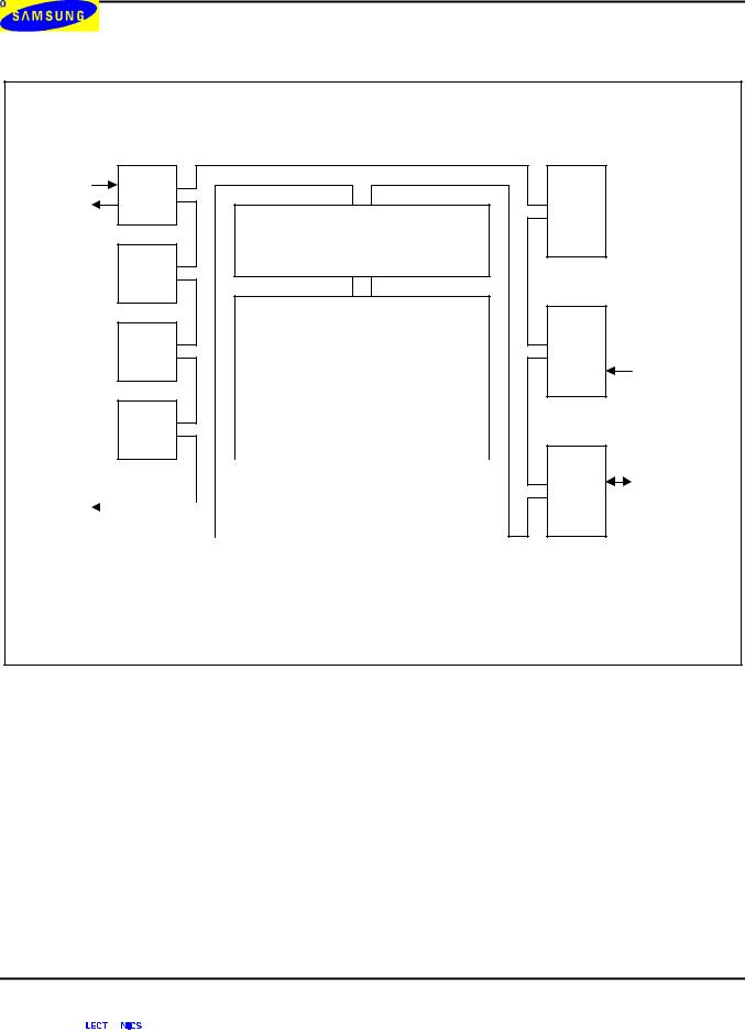
BLOCK DIAGRAM
XIN
OSC
XOUT
Port I/O and
Interrupt Control
Basic
Timer
Timer 0
88RCRI SAMRI CPU
ADC0-ADC8  ADC
ADC
|
|
|
|
|
|
|
|
|
|
|
|
|
P0.6/PWM |
|
PWM |
|
|
|
2 KB ROM |
|
208 Byte |
||||
|
|
|
|
|
||||||||
|
|
|
|
4 KB ROM |
|
Register file |
||||||
|
|
|
|
|
|
|
||||||
|
|
|
|
|
|
|
|
|
|
|
|
|
NOTE: P1.2 is used as input only
Figure 1-1. Block Diagram
PRODUCT OVERVIEW

 P0.0/ADC0/INT0

 P0.1/ADC1/INT1 Port 0
 P0.2/ADC2
...

 P0.7/ADC7

 P1.0
P1.0
Port 1 
 P1.1
P1.1
P1.2

 P2.0/T0
P2.1
Port 2 ...

 P2.6
P2.6
1-3
PRODUCT OVERVIEW |
S3C9442/C9444/F9444/C9452/C9454/F9454 |
|
|
PIN ASSIGNMENTS
VSS
XIN/P1.0
XOUT/P1.1
RESET/P1.2
P2.0/T0
P2.1
P2.2
P2.3
P2.4
P2.5
1 |
|
20 |
VDD |
2 |
|
19 |
P0.0/ADC0/INT0 |
3 |
|
18 |
P0.1/ADC1/INT1 |
4 |
|
17 |
P0.2/ADC2 |
5 |
S3C9452/C9454 16 |
P0.3/ADC3 |
|
6 |
(20-DIP-300A/ |
15 |
P0.4/ADC4 |
|
|
|
|
7 |
20-SOP-375) |
14 |
P0.5/ADC5 |
8 |
|
13 |
P0.6/ADC6/PWM |
9 |
|
12 |
P0.7/ADC7 |
10 |
|
11 |
P2.6/ADC8/CLO |
Figure 1-2. Pin Assignment Diagram (20-Pin DIP/SOP Package)
1-4
S3C9442/C9444/F9444/C9452/C9454/F9454 |
|
PRODUCT OVERVIEW |
|
|
|
|
|
|
|
|
|
VSS
XIN/P1.0
XOUT/P1.1
RESET/P1.2
P2.0/T0
P2.1
P2.2
P2.3
1 |
|
16 |
VDD |
2 |
|
15 |
P0.0/ADC0/INT0 |
3 |
|
14 |
P0.1/ADC1/INT1 |
4 |
S3C9452/C9454 13 |
P0.2/ADC2 |
|
5 |
(16-DIP-300A) |
12 |
P0.3/ADC3 |
6 |
|
11 |
P0.4/ADC4 |
7 |
|
10 |
P0.5/ADC5 |
8 |
|
9 |
P0.6/ADC6/PWM |
Figure 1-3. Pin Assignment Diagram (16-Pin DIP Package)
|
|
|
|
|
|
|
|
|
VSS |
|
1 |
S3C9442/C9444 |
8 |
|
VDD |
||
|
|
|||||||
|
|
|||||||
XIN/P1.0 |
|
2 |
7 |
|
P0.0/ADC0/INT0 |
|||
|
(8-DIP-300 |
|
||||||
|
|
|||||||
|
|
|||||||
XOUT/P1.1 |
|
3 |
6 |
|
P0.1/ADC1/INT1 |
|||
|
8-SOP-225) |
|
||||||
|
|
|||||||
|
|
|
|
|
|
|||
RESET/P1.2 |
|
4 |
|
|
|
5 |
|
P0.2/ADC2 |
|
|
|
|
|
||||
|
|
|
|
|
||||
|
|
|
|
|
|
|
|
|
Figure 1-4. Pin Assignment Diagram (8-Pin DIP/SOP Package)
1-5

PRODUCT OVERVIEW S3C9442/C9444/F9444/C9452/C9454/F9454
PIN DESCRIPTIONS
Table 1-1. S3C9452/C9454 Pin Descriptions
Pin |
In/Out |
Pin Description |
Pin |
Share |
Name |
|
|
Type |
Pins |
|
|
|
|
|
P0.0–P0.7 |
I/O |
Bit-programmable I/O port for Schmitt trigger input or |
E-1 |
ADC0–ADC7 |
|
|
push-pull output. Pull-up resistors are assignable by |
|
INT0/INT1 |
|
|
software. Port0 pins can also be used as A/D converter |
|
PWM |
|
|
input, PWM output or external interrupt input. |
|
|
|
|
|
|
|
P1.0–P1.1 |
I/O |
Bit-programmable I/O port for Schmitt trigger input or |
E-2 |
XIN, XOUT |
|
|
push-pull, open-drain output. Pull-up resistors or pull-down |
|
|
|
|
resistors are assignable by software. |
|
|
|
|
|
|
|
P1.2 |
I |
Schmitt trigger input port |
B |
RESET |
|
|
|
|
|
P2.0–P2.6 |
I/O |
Bit-programmable I/O port for Schmitt trigger input or |
E |
– |
|
|
push-pull, open-drain output. Pull-up resistors are |
|
ADC8/CLO |
|
|
assignable by software. |
E-1 |
T0 |
|
|
|
|
|
XIN, XOUT |
– |
Crystal/Ceramic, or RC oscillator signal for system clock. |
|
P1.0–P1.1 |
RESET |
I |
Internal LVR or External RESET |
B |
P1.2 |
|
|
|
|
|
VDD, VSS |
– |
Voltage input pin and ground |
|
– |
CLO |
O |
System clock output port |
E-1 |
P2.6 |
|
|
|
|
|
INT0–INT1 |
I |
External interrupt input port |
E-1 |
P0.0, P0.1 |
|
|
|
|
|
PWM |
O |
8-Bit high speed PWM output |
E-1 |
P0.6 |
|
|
|
|
|
T0 |
O |
Timer0 match output |
E-1 |
P2.0 |
|
|
|
|
|
ADC0–ADC8 |
I |
A/D converter input |
E-1 |
P0.0–P0.7 |
|
|
|
E |
P2.6 |
|
|
|
|
|
1-6
S3C9442/C9444/F9444/C9452/C9454/F9454 |
PRODUCT OVERVIEW |
|
|
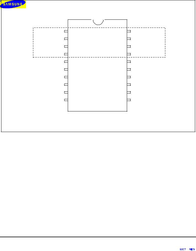
PIN CIRCUITS
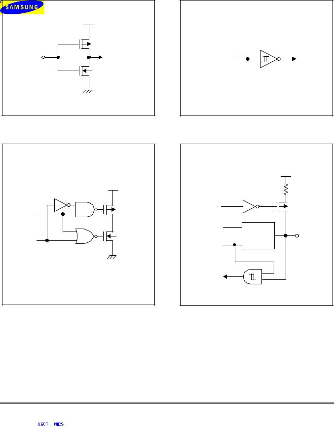
VDD
P-channel
IN
N-channel
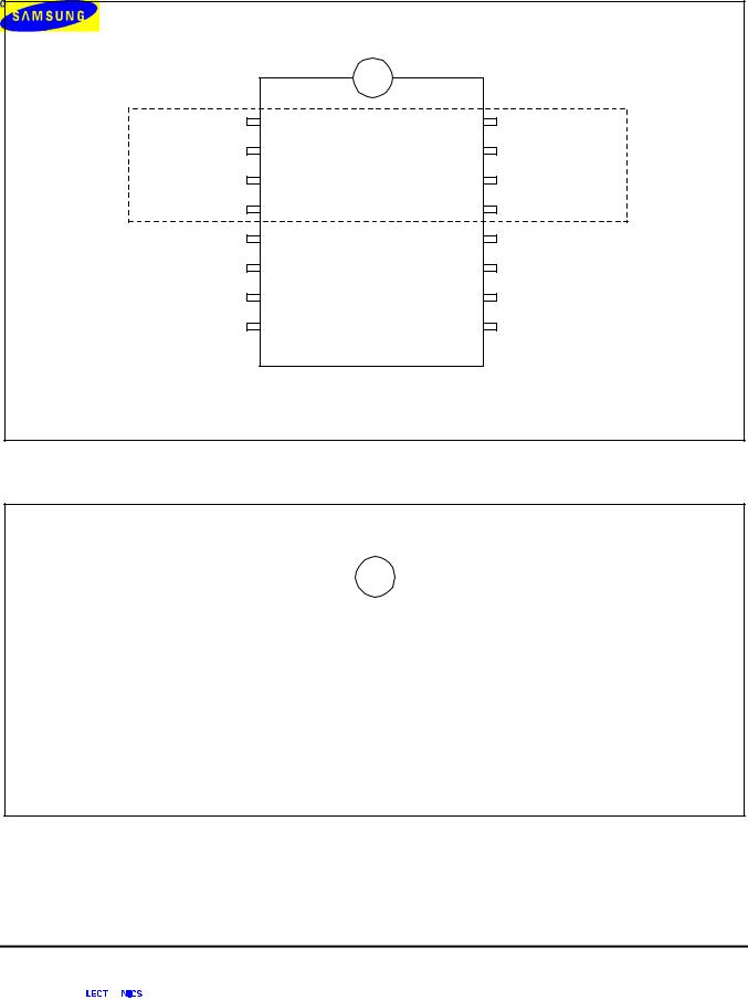
Figure 1-5. Pin Circuit Type A
VDD
Data

 Out
Out
Output
DIsable
Figure 1-7. Pin Circuit Type C
IN 
Figure 1-6. Pin Circuit Type B
VDD
Pull-up |
|
|
|
Enable |
|
|
|
Data |
Circuit |
|
|
|
I/O |
||
Output |
Type C |
||
|
|||
|
|
||
Disable |
|
|
|
Digital |
|
|
|
Input |
|
|
Figure 1-8. Pin Circuit Type D
1-7

PRODUCT OVERVIEW |
S3C9442/C9444/F9444/C9452/C9454/F9454 |
|
|
|
|
VDD |
|
|
|
Open-drain |
|
|
|
Enable |
|
|
|
|
Pull-up |
|
P2CONH |
VDD |
enable |
|
P2CONL |
|
|
Alternative |
M |
P-CH |
|
Output |
Data |
|
|
P2.x |
U |
|
I/O |
X |
N-CH |
|
|
|
|
|
|
Output Disable |
|
|
|
|
(Input Mode) |
|
|
|
Digital |
|
|
|
Input |
|
|
|
Analog Input |
|
|
|
Enable |
|
|
|
ADC |
|
|
Figure 1-9. Pin Circuit Type E
VDD
|
|
|
Pull-up |
|
P0CONH |
VDD |
enable |
|
|
|
|
Alternative |
M |
P-CH |
|
Output |
Data |
|
|
P0.x |
U |
|
I/O |
X |
N-CH |
|
|
|
|
|
|
Output Disable |
|
|
|
|
(Input Mode) |
|
|
|
Digital Input |
|
|
|
Interrupt Input |
|
|
|
Analog Input |
|
|
|
Enable |
|
|
|
ADC |
|
|
|
|
Figure 1-10. Pin Circuit Type E-1 |
|
1-8
 Loading...