


 Loading...
Rev. 1.1, Apr. 2014
M378B5173EB0
M378B1G73EB0
240pin Unbuffered DIMM
based on 4Gb E-die |
1.35V |
|
78FBGA with Lead-Free & Halogen-Free (RoHS compliant)
datasheet
SAMSUNG ELECTRONICS RESERVES THE RIGHT TO CHANGE PRODUCTS, INFORMATION AND
SPECIFICATIONS WITHOUT NOTICE.
Products and specifications discussed herein are for reference purposes only. All information discussed herein is provided on an "AS IS" basis, without warranties of any kind.
This document and all information discussed herein remain the sole and exclusive property of Samsung Electronics. No license of any patent, copyright, mask work, trademark or any other intellectual property right is granted by one party to the other party under this document, by implication, estoppel or otherwise.
Samsung products are not intended for use in life support, critical care, medical, safety equipment, or similar applications where product failure could result in loss of life or personal or physical harm, or any military or defense application, or any governmental procurement to which special terms or provisions may apply.
For updates or additional information about Samsung products, contact your nearest Samsung office.
All brand names, trademarks and registered trademarks belong to their respective owners.
© 2015 Samsung Electronics Co., Ltd.GG All rights reserved.
- 1 -

Unbuffered DIMM
datasheet
Rev. 1.1
DDR3L SDRAM
Revision History
Revision No. |
History |
Draft Date |
Remark |
Editor |
1.0 |
- First SPEC Release |
Oct. 2014 |
- |
J.Y.Lee |
1.1 |
- Added to 1866(13-13-13) speed from Product line-up |
Apr. 2015 |
- |
J.Y.Lee |
- 2 -
Unbuffered DIMM
datasheet
Rev. 1.1
DDR3L SDRAM
Table Of Contents |
|
|
240pin Unbuffered DIMM based on 4Gb E-die |
|
|
1. DDR3L Unbuffered DIMM Ordering Information........................................................................................................... |
4 |
|
2. Key Features................................................................................................................................................................. |
4 |
|
3. Address Configuration .................................................................................................................................................. |
4 |
|
4. x64 DIMM Pin Configurations (Front side/Back side) ................................................................................................... |
5 |
|
5. Pin Description ............................................................................................................................................................. |
6 |
|
6. SPD and Thermal Sensor for ECC UDIMMs ................................................................................................................ |
6 |
|
7. Input/Output Functional Description.............................................................................................................................. |
7 |
|
7.1 Address Mirroring Feature....................................................................................................................................... |
8 |
|
7.1.1. DRAM Pin Wiring Mirroring .............................................................................................................................. |
8 |
|
8. Function Block Diagram:............................................................................................................................................... |
9 |
|
8.1 4GB, 512Mx64 Non ECC Module (Populated as 1 rank of x8 DDR3 SDRAMs)..................................................... |
9 |
|
8.2 8GB, 1Gx64 Non ECC Module (Populated as 2 ranks of x8 DDR3 SDRAMs) ....................................................... |
10 |
|
9. Absolute Maximum Ratings .......................................................................................................................................... |
14 |
|
9.1 Absolute Maximum DC Ratings............................................................................................................................... |
14 |
|
9.2 DRAM Component Operating Temperature Range ................................................................................................ |
14 |
|
10. AC & DC Operating Conditions................................................................................................................................... |
14 |
|
10.1 |
Recommended DC Operating Conditions ............................................................................................................. |
14 |
11. AC & DC Input Measurement Levels .......................................................................................................................... |
15 |
|
11.1 |
AC & DC Logic Input Levels for Single-ended Signals.......................................................................................... |
15 |
11.2 |
VREF Tolerances .................................................................................................................................................. |
17 |
11.3 |
AC and DC Logic Input Levels for Differential Signals .......................................................................................... |
18 |
11.3.1. Differential Signals Definition ......................................................................................................................... |
18 |
|
11.3.2. Differential Swing Requirement for Clock (CK - CK) and Strobe (DQS - DQS) ............................................. |
18 |
|
11.3.3. Single-ended Requirements for Differential Signals ...................................................................................... |
20 |
|
11.3.4. Differential Input Cross Point Voltage ............................................................................................................ |
21 |
|
11.4 |
Slew Rate Definition for Single Ended Input Signals............................................................................................. |
22 |
11.5 |
Slew rate definition for Differential Input Signals ................................................................................................... |
22 |
12. AC & DC Output Measurement Levels ....................................................................................................................... |
22 |
|
12.1 |
Single Ended AC and DC Output Levels............................................................................................................... |
22 |
12.2 |
Differential AC and DC Output Levels ................................................................................................................... |
22 |
12.3 |
Single-ended Output Slew Rate ............................................................................................................................ |
23 |
12.4 |
Differential Output Slew Rate ................................................................................................................................ |
24 |
13. IDD specification definition.......................................................................................................................................... |
25 |
|
14. IDD SPEC Table ......................................................................................................................................................... |
27 |
|
15. Input/Output Capacitance ........................................................................................................................................... |
29 |
|
16. Electrical Characteristics and AC timing ..................................................................................................................... |
30 |
|
16.1 |
Refresh Parameters by Device Density................................................................................................................. |
30 |
16.2 |
Speed Bins and CL, tRCD, tRP, tRC and tRAS for Corresponding Bin ................................................................ |
30 |
16.3 |
Speed Bins and CL, tRCD, tRP, tRC and tRAS for Corresponding Bin ................................................................ |
30 |
16.3.1. Speed Bin Table Notes .................................................................................................................................. |
34 |
|
17. Timing Parameters by Speed Grade .......................................................................................................................... |
35 |
|
17.1 |
Jitter Notes ............................................................................................................................................................ |
39 |
17.2 |
Timing Parameter Notes........................................................................................................................................ |
40 |
18. Physical Dimensions................................................................................................................................................... |
41 |
|
18.1 |
512Mbx8 based 512Mx64 Module (1 Rank) - M378B5173EB0 ............................................................................ |
41 |
18.2 |
512Mbx8 based 1Gx64 Module (2 Ranks) - M378B1G73EB0.............................................................................. |
42 |
- 3 -

Unbuffered DIMM
datasheet
Rev. 1.1
DDR3L SDRAM
1. DDR3L Unbuffered DIMM Ordering Information
Part Number2 |
Density |
Organization |
Component Composition1 |
Number of |
Height |
|
Rank |
||||||
|
|
|
|
|
||
M378B5173EB0-YK0/MA |
4GB |
512Mx64 |
512Mx8(K4B4G0846E-BY##)*8 |
1 |
30mm |
|
M378B1G73EB0-YK0/MA |
8GB |
1Gx64 |
512Mx8(K4B4G0846E-BY##)*16 |
2 |
30mm |
NOTE :
1."##" - K0/MA
2.K0(1600Mbps 11-11-11) / CMA(1866Mbps 13-13-13)
-DDR3-1866(13-13-13) is backward compatible to DDR3-1600(11-11-11)
2. Key Features
Speed |
DDR3-800 |
DDR3-1066 |
DDR3-1333 |
DDR3-1600 |
DDR3-1866 |
Unit |
|
6-6-6 |
7-7-7 |
9-9-9 |
11-11-11 |
13-13-13 |
|||
|
|
||||||
tCK(min) |
2.5 |
1.875 |
1.5 |
1.25 |
1.071 |
ns |
|
|
|
|
|
|
|
|
|
CAS Latency |
6 |
7 |
9 |
11 |
13 |
nCK |
|
|
|
|
|
|
|
|
|
tRCD(min) |
15 |
13.125 |
13.5 |
13.75 |
13.91 |
ns |
|
|
|
|
|
|
|
|
|
tRP(min) |
15 |
13.125 |
13.5 |
13.75 |
13.91 |
ns |
|
|
|
|
|
|
|
|
|
tRAS(min) |
37.5 |
37.5 |
36 |
35 |
34 |
ns |
|
|
|
|
|
|
|
|
|
tRC(min) |
52.5 |
50.625 |
49.5 |
48.75 |
47.91 |
ns |
|
|
|
|
|
|
|
|
•JEDEC standard 1.35V(1.28V~1.14V) & 1.5V(1.425V~1.575V) Power Supply
•VDDQ = 1.35V(1.28V~1.14V) & 1.5V(1.425V~1.575V)
•400MHz fCK for 800Mb/sec/pin, 533MHz fCK for 1066Mb/sec/pin, 667MHz fCK for 1333Mb/sec/pin, 800MHz fCK for 1600Mb/sec/pin, 933MHz fCK for 1866Mb/sec/pin
•8 independent internal bank
•Programmable CAS Latency: 6,7,8,9,10,11,13
•Programmable Additive Latency(Posted CAS) : 0, CL - 2, or CL - 1 clock
• Programmable CAS Write Latency(CWL) = 5 (DDR3-800), 6 (DDR3-1066), 7 (DDR3-1333) ,8 (DDR3-1600) and 9(DDR3-1866)
•Burst Length: 8 (Interleave without any limit, sequential with starting address “000” only), 4 with tCCD = 4 which does not allow seamless read or write [either On the fly using A12 or MRS]
•Bi-directional Differential Data Strobe
•On Die Termination using ODT pin
•Average Refresh Period 7.8us at lower then TCASE 85 C, 3.9us at 85 C < TCASE 95 C
•Asynchronous Reset
3. Address Configuration
Organization |
Row Address |
Column Address |
Bank Address |
Auto Precharge |
512Mx8(4Gb) based Module |
A0-A15 |
A0-A9 |
BA0-BA2 |
A10/AP |
|
|
|
|
|
- 4 -

Unbuffered DIMM
datasheet
Rev. 1.1
DDR3L SDRAM
4. x64 DIMM Pin Configurations (Front side/Back side)
Pin |
Front |
Pin |
Back |
Pin |
|
Front |
|
Pin |
Back |
Pin |
Front |
Pin |
Back |
|||||||||||||||||||
1 |
VREFDQ |
121 |
VSS |
42 |
|
|
|
NC |
|
162 |
|
|
NC |
82 |
|
DQ33 |
202 |
VSS |
||||||||||||||
2 |
|
VSS |
122 |
DQ4 |
43 |
|
|
|
NC |
|
163 |
|
|
VSS |
83 |
|
VSS |
203 |
DM4 |
|||||||||||||
3 |
|
DQ0 |
123 |
DQ5 |
44 |
|
|
VSS |
|
164 |
|
|
NC |
84 |
|
|
|
204 |
NC |
|||||||||||||
|
DQS4 |
|||||||||||||||||||||||||||||||
4 |
|
DQ1 |
124 |
VSS |
45 |
|
|
|
NC |
|
165 |
|
|
NC |
85 |
DQS4 |
205 |
VSS |
||||||||||||||
5 |
|
VSS |
125 |
DM0 |
46 |
|
|
|
NC |
|
166 |
|
|
VSS |
86 |
|
VSS |
206 |
DQ38 |
|||||||||||||
6 |
|
|
|
|
126 |
NC |
47 |
|
|
VSS |
|
167 |
NC (TEST)3 |
87 |
|
DQ34 |
207 |
DQ39 |
||||||||||||||
|
DQS0 |
|
||||||||||||||||||||||||||||||
7 |
|
DQS0 |
127 |
VSS |
48 |
|
|
|
NC |
|
168 |
|
|
|
|
|
|
|
|
|
|
88 |
|
DQ35 |
208 |
VSS |
||||||
|
|
Reset |
|
|||||||||||||||||||||||||||||
8 |
|
VSS |
128 |
DQ6 |
|
|
|
|
|
|
|
|
KEY |
|
|
|
|
|
|
|
|
|
|
89 |
|
VSS |
209 |
DQ44 |
||||
9 |
|
DQ2 |
129 |
DQ7 |
49 |
|
|
|
NC |
|
169 |
CKE1,NC1 |
90 |
|
DQ40 |
210 |
DQ45 |
|||||||||||||||
10 |
|
DQ3 |
130 |
VSS |
50 |
|
CKE0 |
|
170 |
|
|
VDD |
91 |
|
DQ41 |
211 |
VSS |
|||||||||||||||
11 |
|
VSS |
131 |
DQ12 |
51 |
|
|
VDD |
|
171 |
|
|
A15 |
92 |
|
VSS |
212 |
DM5 |
||||||||||||||
12 |
|
DQ8 |
132 |
DQ13 |
52 |
|
|
BA2 |
|
172 |
|
|
A14 |
93 |
|
|
|
213 |
NC |
|||||||||||||
|
|
|
DQS5 |
|||||||||||||||||||||||||||||
13 |
|
DQ9 |
133 |
VSS |
53 |
|
|
|
NC |
|
173 |
|
|
VDD |
94 |
|
DQS5 |
214 |
VSS |
|||||||||||||
14 |
|
VSS |
134 |
DM1 |
54 |
|
|
VDD |
|
174 |
|
|
|
|
|
|
|
|
|
|
95 |
|
VSS |
215 |
DQ46 |
|||||||
|
A12/BC |
|
||||||||||||||||||||||||||||||
15 |
|
|
|
135 |
NC |
55 |
|
|
A11 |
|
175 |
|
|
A9 |
96 |
|
DQ42 |
216 |
DQ47 |
|||||||||||||
|
DQS1 |
|
|
|||||||||||||||||||||||||||||
16 |
|
DQS1 |
136 |
VSS |
56 |
|
|
|
A7 |
|
176 |
|
|
VDD |
97 |
|
DQ43 |
217 |
VSS |
|||||||||||||
17 |
|
VSS |
137 |
DQ14 |
57 |
|
|
VDD |
|
177 |
|
|
A8 |
98 |
|
VSS |
218 |
DQ52 |
||||||||||||||
18 |
|
DQ10 |
138 |
DQ15 |
58 |
|
|
|
A5 |
|
178 |
|
|
A6 |
99 |
|
DQ48 |
219 |
DQ53 |
|||||||||||||
|
|
|
|
|
|
|
|
|
|
|
|
|
|
|
|
|
|
|
|
|||||||||||||
19 |
|
DQ11 |
139 |
VSS |
59 |
|
|
|
A4 |
|
179 |
|
|
VDD |
100 |
|
DQ49 |
220 |
VSS |
|||||||||||||
20 |
|
VSS |
140 |
DQ20 |
60 |
|
|
VDD |
|
180 |
|
|
A3 |
101 |
|
VSS |
221 |
DM6 |
||||||||||||||
21 |
|
DQ16 |
141 |
DQ21 |
61 |
|
|
|
A2 |
|
181 |
|
|
A1 |
102 |
|
|
|
222 |
NC |
||||||||||||
|
|
|
DQS6 |
|||||||||||||||||||||||||||||
22 |
|
DQ17 |
142 |
VSS |
62 |
|
|
VDD |
|
182 |
|
|
VDD |
103 |
|
DQS6 |
223 |
VSS |
||||||||||||||
23 |
|
VSS |
143 |
DM2 |
63 |
|
CK1,NC |
|
183 |
|
|
VDD |
104 |
|
VSS |
224 |
DQ54 |
|||||||||||||||
24 |
|
|
|
|
144 |
NC |
64 |
|
|
|
|
|
|
|
|
184 |
|
|
CK0 |
105 |
|
DQ50 |
225 |
DQ55 |
||||||||
|
DQS2 |
|
|
CK1,NC |
|
|
||||||||||||||||||||||||||
25 |
|
DQS2 |
145 |
VSS |
65 |
|
|
VDD |
|
185 |
|
|
|
|
|
|
|
|
|
|
106 |
|
DQ51 |
226 |
VSS |
|||||||
|
|
|
|
CK0 |
|
|||||||||||||||||||||||||||
26 |
|
VSS |
146 |
DQ22 |
66 |
|
|
VDD |
|
186 |
|
|
VDD |
107 |
|
VSS |
227 |
DQ60 |
||||||||||||||
27 |
|
DQ18 |
147 |
DQ23 |
67 |
|
VREFCA |
|
187 |
|
|
NC |
108 |
|
DQ56 |
228 |
DQ61 |
|||||||||||||||
28 |
|
DQ19 |
148 |
VSS |
68 |
|
|
|
NC |
|
188 |
|
|
A0 |
109 |
|
DQ57 |
229 |
VSS |
|||||||||||||
29 |
|
VSS |
149 |
DQ28 |
69 |
|
|
VDD |
|
189 |
|
|
VDD |
110 |
|
VSS |
230 |
DM7 |
||||||||||||||
30 |
|
DQ24 |
150 |
DQ29 |
70 |
|
A10/AP |
|
190 |
|
|
BA1 |
111 |
|
|
|
231 |
NC |
||||||||||||||
|
|
|
|
|
DQS7 |
|||||||||||||||||||||||||||
31 |
|
DQ25 |
151 |
VSS |
71 |
|
|
BA0 |
|
191 |
|
|
VDD |
112 |
|
DQS7 |
232 |
VSS |
||||||||||||||
32 |
|
VSS |
152 |
DM3 |
72 |
|
|
VDD |
|
192 |
|
|
|
|
|
|
|
|
113 |
|
VSS |
233 |
DQ62 |
|||||||||
|
|
|
|
RAS |
|
|||||||||||||||||||||||||||
33 |
|
|
|
153 |
NC |
73 |
|
|
|
|
|
|
|
|
193 |
|
|
|
|
|
|
|
|
|
|
114 |
|
DQ58 |
234 |
DQ63 |
||
|
DQS3 |
|
WE |
|
|
S0 |
|
|||||||||||||||||||||||||
34 |
|
DQS3 |
154 |
VSS |
74 |
|
|
|
|
|
|
|
|
194 |
|
|
VDD |
115 |
|
DQ59 |
235 |
VSS |
||||||||||
|
|
|
CAS |
|
|
|
||||||||||||||||||||||||||
35 |
|
VSS |
155 |
DQ30 |
75 |
|
|
VDD |
|
195 |
ODT0 |
116 |
|
VSS |
236 |
VDDSPD |
||||||||||||||||
36 |
|
DQ26 |
156 |
DQ31 |
76 |
|
S1, NC1 |
|
196 |
|
|
A13 |
117 |
|
SA0 |
237 |
SA1 |
|||||||||||||||
37 |
|
DQ27 |
157 |
VSS |
77 |
ODT1, NC1 |
|
197 |
|
|
VDD |
118 |
|
SCL |
238 |
SDA |
||||||||||||||||
38 |
|
VSS |
158 |
NC |
78 |
|
|
VDD |
|
198 |
|
|
NC |
119 |
|
SA2 |
239 |
VSS |
||||||||||||||
39 |
|
NC |
159 |
NC |
79 |
|
|
|
NC |
|
199 |
|
|
VSS |
120 |
|
VTT |
240 |
VTT |
|||||||||||||
40 |
|
NC |
160 |
VSS |
80 |
|
|
VSS |
|
200 |
|
DQ36 |
|
|
|
|
|
|
||||||||||||||
41 |
|
VSS |
161 |
NC |
81 |
|
DQ32 |
|
201 |
DQ37 |
|
|
|
|
|
|
||||||||||||||||
NOTE :
NC = No Connect; NU = Not Used; RFU = Reserved Future Use
1.S1, ODT1, CKE1: Used for dual-rank UDIMMs; NC on single-rank UDIMMs
2.CK1,NC and CK1,NC : Used for dual-rank UDIMMs; not used on single-rank UDIMMs, but terminated
3.TEST (pin 167) used by memory bus analysis tools (unused on memory DIMMs)
SAMSUNG ELECTRONICS CO., Ltd. reserves the right to change products and specifications without notice.
- 5 -
Unbuffered DIMM
datasheet
Rev. 1.1
DDR3L SDRAM
5. Pin Description
|
Pin Name |
Description |
|
Pin Name |
Description |
|||||||||||
A0-A15 |
SDRAM address bus |
SCL |
I2C serial bus clock for EEPROM |
|||||||||||||
|
BA0-BA2 |
SDRAM bank select |
SDA |
I2C serial bus data line for EEPROM |
||||||||||||
|
|
|
|
|
|
|
|
|
|
|
|
SDRAM row address strobe |
SA0-SA2 |
I2C serial address select for EEPROM |
||
|
RAS |
|||||||||||||||
|
|
|
|
|
|
|
|
|
|
|
|
SDRAM column address strobe |
|
VDD* |
SDRAM core power supply |
|
|
CAS |
|||||||||||||||
|
|
|
|
|
|
|
|
|
|
|
SDRAM write enable |
|
VDDQ* |
SDRAM I/O Driver power supply |
||
|
WE |
|||||||||||||||
|
|
|
|
|
|
|
|
|
|
|
|
DIMM Rank Select Lines |
|
VREFDQ |
SDRAM I/O reference supply |
|
|
S0, S1 |
|||||||||||||||
|
CKE0,CKE1 |
SDRAM clock enable lines |
|
VREFCA |
SDRAM command/address reference supply |
|||||||||||
|
ODT0, ODT1 |
On-die termination control lines |
|
VSS |
Power supply return (ground) |
|||||||||||
|
DQ0 - DQ63 |
DIMM memory data bus |
|
VDDSPD |
Serial EEPROM positive power supply |
|||||||||||
|
CB0 - CB7 |
DIMM ECC check bits |
|
NC |
Spare Pins(no connect) |
|||||||||||
|
|
|
|
|
|
|
|
|
|
|
|
|
|
|
|
|
|
DQS0 - DQS8 |
SDRAM data strobes |
TEST |
Used by memory bus analysis tools |
||||||||||||
|
(positive line of differential pair) |
(unused on memory DIMMs) |
||||||||||||||
|
|
|
|
|
|
|
|
|
|
|
|
|
|
|
||
|
|
|
|
|
|
|
|
|
|
|
|
|
|
|
|
|
|
|
|
|
|
|
|
|
|
|
|
|
SDRAM differential data strobes |
|
|
|
|
|
DQS0-DQS8 |
|
RESET |
Set DRAMs Known State |
||||||||||||
|
(negative line of differential pair) |
|
||||||||||||||
|
|
|
|
|
|
|
|
|
|
|
|
|
|
|
|
|
|
|
|
|
|
|
|
|
|
|
|
|
|
|
|
|
|
|
|
|
|
|
|
|
|
|
|
|
|
SDRAM data masks/high data strobes |
|
|
|
|
|
DM0-DM8 |
|
EVENT |
Reserved for optional temperature-sensing hardware |
||||||||||||
|
(x8-based x72 DIMMs) |
|
||||||||||||||
|
|
|
|
|
|
|
|
|
|
|
|
|
|
|
|
|
|
|
|
|
|
|
|
|
|
|
|
|
|
|
|
|
|
|
CK0, CK1 |
SDRAM clocks |
|
VTT |
SDRAM I/O termination supply |
|||||||||||
|
(positive line of differential pair) |
|
||||||||||||||
|
|
|
|
|
|
|
|
|
|
|
|
|
|
|
|
|
|
|
|
|
|
|
|
|
|
|
|
|
|
|
|
|
|
|
|
|
|
|
|
|
|
|
|
|
|
SDRAM clocks |
|
|
|
|
|
CK0, CK1 |
|
RFU |
Reserved for future use |
||||||||||||
|
(negative line of differential pair) |
|
||||||||||||||
|
|
|
|
|
|
|
|
|
|
|
|
|
|
|
|
|
|
|
|
|
|
|
|||||||||||
NOTE : |
|
|
|
|
|
|||||||||||
*The VDD and VDDQ pins are tied common to a single power-plane on these designs. |
|
|
|
|
||||||||||||
** DQS8, |
|
|
|
|
|
|
|
|||||||||
DQS8, DM8 arefor ECC UDIMM only |
|
|
|
|
||||||||||||
6. SPD and Thermal Sensor for ECC UDIMMs
On DIMM thermal sensor will provide DRAM temperature readout through a integrated thermal sensor.
SCL |
SDA |
EVENT  WP/EVENT
R1 |
|
SA0 |
SA1 |
SA2 |
||
0 |
|
|||||
|
R2 |
|
|
|
|
|
|
0 SA0 |
|
|
|
|
|
|
SA1 |
SA2 |
||||
NOTE :
1.Raw Cards D (1Rx8 ECC) and E (2Rx8 ECC) support a thermal sensor.
2.When the SPD and the thermal sensor are placed on the module, R1 is placed but R2 is not. When only the SPD is placed on the module, R2 is placed but R1 is not.
[ Table 1 ] Temperature Sensor Characteristics
Grade |
Range |
Temperature Sensor Accuracy |
Units |
NOTE |
|||
Min. |
Typ. |
Max. |
|||||
|
|
|
|
||||
|
75 < Ta < 95 |
- |
+/- 0.5 |
+/- 1.0 |
|
- |
|
|
|
|
|
|
|
|
|
B |
40 < Ta < 125 |
- |
+/- 1.0 |
+/- 2.0 |
C |
- |
|
|
|
|
|
|
|
|
|
|
-20 < Ta < 125 |
- |
+/- 2.0 |
+/- 3.0 |
|
- |
|
|
|
|
|
|
|
|
|
|
Resolution |
|
0.25 |
|
C /LSB |
- |
|
|
|
|
|
|
|
|
|
|
|
- 6 - |
|
|
|
|
|

Unbuffered DIMM
datasheet
Rev. 1.1
DDR3L SDRAM
7. Input/Output Functional Description
|
|
|
|
Symbol |
|
Type |
|
|
|
|
|
|
|
|
|
|
|
|
|
|
|
|
|
|
|
Function |
|||||||||
|
|
|
|
|
|
|
|
|
|
|
|
|
CK and |
|
|
are differential clock inputs. All the DDR3 SDRAM addr/cntl inputs are sampled on the crossing of positive |
|||||||||||||||||||
|
CK0-CK1 |
|
|
CK |
|||||||||||||||||||||||||||||||
|
|
|
|
|
|
|
|
|
|
|
|
|
|
|
|
|
|
|
|
|
|
|
|
|
|
|
|||||||||
|
|
SSTL |
|
edge of CK and negative edge of CK. Output (read) data is reference to the crossing of CK and CK (Both directions of |
|||||||||||||||||||||||||||||||
|
|
|
|
|
|
|
|
|
|
|
|
||||||||||||||||||||||||
|
CK0-CK1 |
||||||||||||||||||||||||||||||||||
|
|
|
|
crossing) |
|||||||||||||||||||||||||||||||
|
|
|
|
|
|
|
|
|
|
|
|
|
|||||||||||||||||||||||
|
|
|
|
|
|
|
|
|
|
|
|
|
|||||||||||||||||||||||
|
CKE0-CKE1 |
|
SSTL |
Activates the SDRAM CK signal when high and deactivates the CK signal when low. By deactivating the clocks, CKE low |
|||||||||||||||||||||||||||||||
|
|
|
initiates the Power Down mode, or the Self-Refresh mode |
||||||||||||||||||||||||||||||||
|
|
|
|
|
|
|
|
|
|
|
|
|
|||||||||||||||||||||||
|
|
|
|
|
|
|
|
|
|
|
|
|
|
||||||||||||||||||||||
|
|
|
|
|
|
|
|
|
|
|
|
|
Enables the associated SDRAM command decoder when low and disables the command decoder when high. When the |
||||||||||||||||||||||
|
S0-S1 |
|
SSTL |
|
command decoder is disabled, new command are ignored but previous operations continue. This signal provides for |
||||||||||||||||||||||||||||||
|
|
|
|
|
|
|
|
|
|
|
|
|
external rank selection on systems with multiple ranks. |
||||||||||||||||||||||
|
|
|
|
|
|
|
|
|
|
|
|
|
|
|
|
|
|
|
|
|
|
|
|
|
|||||||||||
|
|
|
|
|
|
|
|
|
|
|
SSTL |
|
|
|
|
|
|
and |
|
(ALONG WITH |
|
|
|
|
|
|
|
|
|
|
|
||||
|
RAS, |
CAS, |
WE |
RAS, |
CAS, |
WE |
S) define the command being entered. |
||||||||||||||||||||||||||||
|
|
|
|
|
|
|
|
|
|
|
|
|
When high, termination resistance is enabled for all DQ, DQS, |
|
and DM pins, assuming the function is enabled in the |
||||||||||||||||||||
|
ODT0-ODT1 |
|
SSTL |
|
DQS |
||||||||||||||||||||||||||||||
|
|
|
Extended Mode Register Set (EMRS). |
||||||||||||||||||||||||||||||||
|
|
|
|
|
|
|
|
|
|
|
|
|
|||||||||||||||||||||||
|
|
|
|
|
|||||||||||||||||||||||||||||||
|
VREFDQ |
|
Supply |
Reference voltage for SSTL 15 I/O inputs. |
|||||||||||||||||||||||||||||||
|
VREFCA |
|
Supply |
Reference voltage for SSTL 15 command/address inputs. |
|||||||||||||||||||||||||||||||
|
VDDQ |
|
Supply |
|
Power supply for the DDR3 SDRAM output buffers to provide improved noise immunity. For all current DDR3 unbuffered |
||||||||||||||||||||||||||||||
|
|
|
DIMM designs, VDDQ shares the same power plane as VDD pins. |
||||||||||||||||||||||||||||||||
|
|
|
|
|
|
|
|
|
|
|
|
|
|||||||||||||||||||||||
|
BA0-BA2 |
|
SSTL |
|
Selects which SDRAM bank of eight is activated. |
||||||||||||||||||||||||||||||
|
|
|
|
|
|
|
|
|
|
|
|
|
|
||||||||||||||||||||||
|
|
|
|
|
|
|
|
|
|
|
|
|
During a Bank Activate command cycle, Address input defines the row address (RA0-RA13) |
||||||||||||||||||||||
|
|
|
|
|
|
|
|
|
|
|
|
|
During a Read or Write command cycle, Address input defines the column address, In addition to the column address, |
||||||||||||||||||||||
|
|
|
|
|
|
|
|
|
|
|
|
AP is used to invoke autoprecharge operation at the end of the burst read or write cycle. If AP is high, autoprecharge is |
|||||||||||||||||||||||
A0-A15 |
|
SSTL |
|
selected and BA0, BA1, BA2 defines the bank to be precharged. If AP is low, autoprecharge is disabled. During a pre- |
|||||||||||||||||||||||||||||||
|
|
charge command cycle, AP is used in conjunction with BA0, BA1, BA2 to control which bank(s) to precharge. If AP is |
|||||||||||||||||||||||||||||||||
|
|
|
|
|
|
|
|
|
|
|
|
|
|||||||||||||||||||||||
|
|
|
|
|
|
|
|
|
|
|
|
|
high, all banks will be precharged regardless of the state of BA0, BA1 or BA2. If AP is low, BA0, BA1 and BA2 are used |
||||||||||||||||||||||
|
|
|
|
|
|
|
|
|
|
|
|
|
|
|
|
|
|
|
is sampled during READ and WRITE commands to determine if burst chop |
||||||||||||||||
|
|
|
|
|
|
|
|
|
|
|
|
|
to define which bank to precharge. A12(BC) |
|
|||||||||||||||||||||
|
|
|
|
|
|
|
|
|
|
|
|
|
(on-the-fly) will be performed (HIGH, no burst chop; Low, burst chopped). |
||||||||||||||||||||||
|
|
|
|
|
|
|
|
|
|
|
|
|
|
|
|
|
|
|
|
|
|
|
|
|
|
|
|
||||||||
|
DQ0-DQ63 |
|
SSTL |
|
Data and Check Bit Input/Output pins. |
||||||||||||||||||||||||||||||
|
CB0-CB7 |
|
|
||||||||||||||||||||||||||||||||
|
|
|
|
|
|
|
|
|
|
|
|
|
|
|
|
|
|
|
|
|
|
|
|
|
|
|
|||||||||
|
|
|
|
|
|
|
|
|
|
|
|
|
|
||||||||||||||||||||||
|
DM0-DM81 |
|
|
|
DM is an input mask signal for write data. Input data is masked when DM is sampled High coincident with that input data |
||||||||||||||||||||||||||||||
|
|
SSTL |
|
during a write access. DM is sampled on both edges of DQS. Although DM pins are input only, the DM loading matches |
|||||||||||||||||||||||||||||||
|
|
|
|
|
|
|
|
|
|
|
|
|
the DQ and DQS loading. |
||||||||||||||||||||||
|
|
|
|
|
|
|
|
|
|
|
|
|
|
||||||||||||||||||||||
|
VDD,VSS |
|
Supply |
|
Power and ground for DDR3 SDRAM input buffers, and core logic. VDD and VDDQ pins are tied to VDD/VDDQ planes on |
||||||||||||||||||||||||||||||
|
|
|
these modules. |
||||||||||||||||||||||||||||||||
|
|
|
|
|
|
|
|
|
|
|
|
|
|||||||||||||||||||||||
|
|
|
|
|
|
|
|
|
|
|
|
|
|
|
|
|
|
|
|
|
|
|
|
|
|
|
|
||||||||
|
DQS0-DQS81 |
|
SSTL |
|
Data strobe for input and output data. |
||||||||||||||||||||||||||||||
|
|
|
|
|
- |
|
|
1 |
|
|
|||||||||||||||||||||||||
|
DQS0 |
DQS8 |
|
|
|
|
|
|
|
|
|
|
|
|
|
|
|
|
|
|
|
|
|
|
|
|
|
|
|||||||
|
SA0-SA2 |
|
- |
These signals and tied at the system planar to either VSS or VDDSPD to configure the serial SPD EERPOM address |
|||||||||||||||||||||||||||||||
|
|
|
range. |
||||||||||||||||||||||||||||||||
|
|
|
|
|
|
|
|
|
|
|
|
|
|||||||||||||||||||||||
|
|
|
|
|
|
|
|
|
|
|
|
|
|||||||||||||||||||||||
|
SDA |
|
- |
This bidirectional pin is used to transfer data into or out of the SPD EEPROM. An external resistor may be connected |
|||||||||||||||||||||||||||||||
|
|
|
from the SDA bus line to VDDSPD to act as a pull-up on the system board. |
||||||||||||||||||||||||||||||||
|
|
|
|
|
|
|
|
|
|
|
|
|
|||||||||||||||||||||||
|
SCL |
|
- |
This signal is used to clock data into and out of the SPD EEPROM. An external resistor may be connected from the SCL |
|||||||||||||||||||||||||||||||
|
|
|
bus time to VDDSPD to act as a pull-up on the system board. |
||||||||||||||||||||||||||||||||
|
|
|
|
|
|
|
|
|
|
|
|
|
|||||||||||||||||||||||
|
VDDSPD |
|
Supply |
|
Power supply for SPD EEPROM. This supply is separate from the VDD/VDDQ power plane. EEPROM supply is operable |
||||||||||||||||||||||||||||||
|
|
|
from 3.0V to 3.6V. |
||||||||||||||||||||||||||||||||
|
|
|
|
|
|
|
|
|
|
|
|
|
|||||||||||||||||||||||
|
|
|
|
|
|
|
|
|
|
||||||||||||||||||||||||||
|
|
|
|
|
|
|
|
- |
The |
|
|
|
|
|
|
pin is connected to the |
|
|
|
|
|
pin on each DRAM. When low, all DRAMs are set to a know state. |
|||||||||||||
|
RESET |
RESET |
RESET |
||||||||||||||||||||||||||||||||
|
|
|
|
|
|
|
|
|
|
|
|
This signal indicates that a thermal event has been detected in the thermal sensing device. The system should guarantee |
|||||||||||||||||||||||
|
EVENT |
|
Output |
||||||||||||||||||||||||||||||||
|
|
|
|
|
|
|
|
|
|
|
|
|
|
|
|
|
|
|
|
|
|
|
|
|
|
||||||||||
|
|
the electrical level requirement is met for the EVENT pin on TS/SPD part |
|||||||||||||||||||||||||||||||||
|
|
|
|
|
|
|
|
|
|
|
|
|
|||||||||||||||||||||||
NOTE :
1. DM8, DQS8 and DQS8 are for ECC UDIMM only
- 7 -
Unbuffered DIMM
datasheet
Rev. 1.1
DDR3L SDRAM
7.1 Address Mirroring Feature
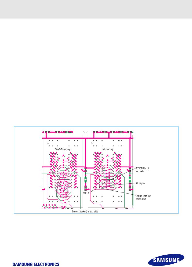
There is a via grid located under the DRAMs for wiring the CA signals (address, bank address, command, and control lines) to the DRAM pins. The length of the traces from the vias to the DRAMs places limitations on the bandwidth of the module. The shorter these traces, the higher the bandwidth. To extend the bandwidth of the CA bus for DDR3 modules, a scheme was defined to reduce the length of these traces.
The pins on the DRAM are defined in a manner that allows for these short trace lengths. The CA bus pins in Columns 2 and 8, ignoring the mechanical support pins, do not have any special functions (secondary functions). This allows the most flexibility with these pins. These are address pins A3, A4, A5, A6, A7, A8 and bank address pins BA0 and BA1. Refer to Table . Rank 0 DRAM pins are wired straight, with no mismatch between the connector pin assignment and the DRAM pin assignment. Some of the Rank 1 DRAM pins are cross wired as defined in the table. Pins not listed in the table are wired straight.
7.1.1 DRAM Pin Wiring Mirroring
Connector Pin |
|
DRAM Pin |
|
Rank 0 |
|
Rank 1 |
|
|
|
||
A3 |
A3 |
|
A4 |
|
|
|
|
A4 |
A4 |
|
A3 |
|
|
|
|
A5 |
A5 |
|
A6 |
|
|
|
|
A6 |
A6 |
|
A5 |
|
|
|
|
A7 |
A7 |
|
A8 |
|
|
|
|
A8 |
A8 |
|
A7 |
|
|
|
|
BA0 |
BA0 |
|
BA1 |
|
|
|
|
BA1 |
BA1 |
|
BA0 |
|
|
|
|
Figure 1illustrates the wiring in both the mirrored and non-mirrored case. The lengths of the traces to the DRAM pins, is obviously shorter. The via grid is smaller as well.
Figure 1. Wiring Differences for Mirrored and Non-Mirrored Addresses
Since the cross-wired pins have no secondary functions, there is no problem in normal operation. Any data written is read the same way. There are limitations however. When writing to the internal registers with a "load mode" operation, the specific address is required. See the DDR3 UDIMM SPD specification for these details. The controller must read the SPD and have the capability of de-mirroring the address when accessing the second rank. SAMSUNG DDR3 dual rank UDIMM R/C B(2Rx8) and R/C E(2Rx8) Modules are using Mirrored Addresses mode.
- 8 -

Unbuffered DIMM
datasheet
Rev. 1.1
DDR3L SDRAM
8. Function Block Diagram:
8.1 4GB, 512Mx64 Non ECC Module (Populated as 1 rank of x8 DDR3 SDRAMs)
S0
DQS0 
DQS0 
DM0
|
DM |
CS |
DQS DQS |
DQ0 |
I/O 0 |
D0 |
|
DQ1 |
I/O 1 |
|
|
DQ2 |
I/O 2 |
|
|
DQ3 |
I/O 3 |
|
|
DQ4 |
I/O 4 |
|
|
DQ5 |
I/O 5 |
|
ZQ |
DQ6 |
I/O 6 |
|
|
DQ7 |
I/O 7 |
|
|
DQS1 |
|
|
|
DQS1 |
|
|
|
DM1 |
|
|
|
|
DM |
CS |
DQS DQS |
DQ8 |
I/O 0 |
|
|
DQ9 |
I/O 1 |
D1 |
|
DQ10 |
I/O 2 |
|
|
DQ11 |
I/O 3 |
|
|
DQ12 |
I/O 4 |
|
|
DQ13 |
I/O 5 |
|
ZQ |
DQ14 |
I/O 6 |
|
|
DQ15 |
I/O 7 |
|
|
DQS2 |
|
|
|
DQS2 |
|
|
|
DM2 |
|
|
|
|
DM |
CS |
DQS DQS |
DQ16 |
I/O 0 |
D2 |
|
DQ17 |
I/O 1 |
|
|
DQ18 |
I/O 2 |
|
|
DQ19 |
I/O 3 |
|
|
DQ20 |
I/O 4 |
|
|
DQ21 |
I/O 5 |
|
ZQ |
DQ22 |
I/O 6 |
|
|
DQ23 |
I/O 7 |
|
|
DQS3 |
|
|
|
DQS3 |
|
|
|
DM3 |
|
|
|
|
DM NU/ |
CS |
DQS DQS |
DQ24 |
I/O 0 |
D3 |
|
DQ25 |
I/O 1 |
|
|
DQ26 |
I/O 2 |
|
|
DQ27 |
I/O 3 |
|
|
DQ28 |
I/O 4 |
|
|
DQ29 |
I/O 5 |
|
ZQ |
DQ30 |
I/O 6 |
|
|
DQ31 |
I/O 7 |
|
|
BA0 - BA2  BA0-BA2 : SDRAMs D0 - D7
A0 - A13  A0-A13 : SDRAMs D0 - D7
RAS  RAS : SDRAMs D0 - D7
CAS  CAS : SDRAMs D0 - D7
CKE0  CKE : SDRAMs D0 - D7
WE  WE : SDRAMs D0 - D7
ODT0  ODT : SDRAMs D0 - D7
CK0  CK : SDRAMs D0 - D7
DQS4  DQS4
DQS4  DM4
DM4 
|
DM |
CS |
DQS DQS |
DQ32 |
I/O 0 |
D4 |
|
DQ33 |
I/O 1 |
|
|
DQ34 |
I/O 2 |
|
|
DQ35 |
I/O 3 |
|
|
DQ36 |
I/O 4 |
|
|
DQ37 |
I/O 5 |
|
ZQ |
DQ38 |
I/O 6 |
|
|
DQ39 |
I/O 7 |
|
|
DQS5 |
|
|
|
DQS5 |
|
|
|
DM5 |
|
|
|
|
DM |
CS |
DQS DQS |
DQ40 |
I/O 0 |
D5 |
|
DQ41 |
I/O 1 |
|
|
DQ42 |
I/O 2 |
|
|
DQ43 |
I/O 3 |
|
|
DQ44 |
I/O 4 |
|
|
DQ45 |
I/O 5 |
|
ZQ |
DQ46 |
I/O 6 |
|
|
DQ47 |
I/O 7 |
|
|
DQS6 |
|
|
|
DQS6 |
|
|
|
DM6 |
|
|
|
|
DM |
CS |
DQS DQS |
DQ48 |
I/O 0 |
D6 |
|
DQ49 |
I/O 1 |
|
|
DQ50 |
I/O 2 |
|
|
DQ51 |
I/O 3 |
|
|
DQ52 |
I/O 4 |
|
|
DQ53 |
I/O 5 |
|
ZQ |
DQ54 |
I/O 6 |
|
|
DQ55 |
I/O 7 |
|
|
DQS7 |
|
|
|
DQS7 |
|
|
|
DM7 |
|
|
|
Serial PD
SCL |
|
|
WP |
|
SDA |
A0 |
A1 |
A2 |
SA0 |
SA1 |
SA2 |
|
DM |
CS DQS DQS |
DQ56 |
I/O 0 |
D7 |
DQ57 |
I/O 1 |
|
DQ58 |
I/O 2 |
|
DQ59 |
I/O 3 |
|
DQ60 |
I/O 4 |
|
DQ61 |
I/O 5 |
ZQ |
DQ62 |
I/O 6 |
|
DQ63 |
I/O 7 |
|
NOTE :
1.For each DRAM, a unique ZQ resistor is connected to ground. The ZQ resistor is 240 Ohm +/- 1%
2.One SPD exists per module.
VDDSPD |
SPD |
VDD/VDDQ  D0 - D7
VREFDQ  D0 - D7
VSS  D0 - D7
VREFCA  D0 - D7
- 9 -

Unbuffered DIMM
datasheet
Rev. 1.1
DDR3L SDRAM
8.2 8GB, 1Gx64 Non ECC Module (Populated as 2 ranks of x8 DDR3 SDRAMs)
S1 |
|
|
|
|
|
|
|
|
|
|
S0 |
|
|
|
|
|
|
|
|
|
|
DQS0 |
|
|
|
|
|
|
DQS4 |
|
|
|
DQS0 |
|
|
|
|
|
|
DQS4 |
|
|
|
DM0 |
|
|
|
|
|
|
DM4 |
|
|
|
DQ0 |
DM |
CS |
DQS DQS |
DM |
CS |
DQS DQS |
DQ32 |
DM |
CS |
DQS DQS |
I/O 0 |
D0 |
|
I/O 0 |
D8 |
|
I/O 0 |
D4 |
|
||
DQ1 |
I/O 1 |
|
I/O 1 |
|
DQ33 |
I/O 1 |
|
|||
DQ2 |
I/O 2 |
|
|
I/O 2 |
|
|
DQ34 |
I/O 2 |
|
|
DQ3 |
I/O 3 |
|
|
I/O 3 |
|
|
DQ35 |
I/O 3 |
|
|
DQ4 |
I/O 4 |
|
|
I/O 4 |
|
|
DQ36 |
I/O 4 |
|
|
DQ5 |
I/O 5 |
|
|
I/O 5 |
|
|
DQ37 |
I/O 5 |
|
|
DQ6 |
I/O 6 |
|
|
I/O 6 |
|
|
DQ38 |
I/O 6 |
|
|
DQ7 |
I/O 7 |
|
ZQ |
I/O 7 |
|
ZQ |
DQ39 |
I/O 7 |
|
ZQ |
|
|
|
|
|
|
|
|
|||
DQS1 |
|
|
|
|
|
|
DQS5 |
|
|
|
DQS1 |
|
|
|
|
|
|
DQS5 |
|
|
|
DM1 |
|
|
|
|
|
|
DM5 |
|
|
|
DQ8 |
DM |
CS |
DQS DQS |
DM |
CS |
DQS DQS |
DQ40 |
DM |
CS |
DQS DQS |
I/O 0 |
D1 |
|
I/O 0 |
D9 |
|
I/O 0 |
D5 |
|
||
DQ9 |
I/O 1 |
|
I/O 1 |
|
DQ41 |
I/O 1 |
|
|||
DQ10 |
I/O 2 |
|
|
I/O 2 |
|
|
DQ42 |
I/O 2 |
|
|
DQ11 |
I/O 3 |
|
|
I/O 3 |
|
|
DQ43 |
I/O 3 |
|
|
DQ12 |
I/O 4 |
|
|
I/O 4 |
|
|
DQ44 |
I/O 4 |
|
|
DQ13 |
I/O 5 |
|
|
I/O 5 |
|
|
DQ45 |
I/O 5 |
|
|
DQ14 |
I/O 6 |
|
|
I/O 6 |
|
|
DQ46 |
I/O 6 |
|
|
DQ15 |
I/O 7 |
|
ZQ |
I/O 7 |
|
ZQ |
DQ47 |
I/O 7 |
|
ZQ |
|
|
|
|
|
|
|
|
|||
DQS2 |
|
|
|
|
|
|
DQS6 |
|
|
|
DQS2 |
|
|
|
|
|
|
DQS6 |
|
|
|
DM2 |
|
|
|
|
|
|
DM6 |
|
|
|
DQ16 |
DM |
CS |
DQS DQS |
DM |
CS |
DQS DQS |
DQ48 |
DM |
CS |
DQS DQS |
I/O 0 |
D2 |
|
I/O 0 |
D10 |
I/O 0 |
D6 |
|
|||
DQ17 |
I/O 1 |
|
I/O 1 |
DQ49 |
I/O 1 |
|
||||
DQ18 |
I/O 2 |
|
|
I/O 2 |
|
|
DQ50 |
I/O 2 |
|
|
DQ19 |
I/O 3 |
|
|
I/O 3 |
|
|
DQ51 |
I/O 3 |
|
|
DQ20 |
I/O 4 |
|
|
I/O 4 |
|
|
DQ52 |
I/O 4 |
|
|
DQ21 |
I/O 5 |
|
|
I/O 5 |
|
|
DQ53 |
I/O 5 |
|
|
DQ22 |
I/O 6 |
|
|
I/O 6 |
|
|
DQ54 |
I/O 6 |
|
|
DQ23 |
I/O 7 |
|
ZQ |
I/O 7 |
|
ZQ |
DQ55 |
I/O 7 |
|
ZQ |
|
|
|
|
|
|
|
|
|||
DQS3 |
|
|
|
|
|
|
DQS7 |
|
|
|
DQS3 |
|
|
|
|
|
|
DQS7 |
|
|
|
DM3 |
|
|
|
|
|
|
DM7 |
|
|
|
DQ24 |
DM |
CS |
DQS DQS |
DM |
CS |
DQS DQS |
DQ56 |
DM |
CS |
DQS DQS |
I/O 0 |
D3 |
|
I/O 0 |
D11 |
I/O 0 |
D7 |
|
|||
DQ25 |
I/O 1 |
|
I/O 1 |
DQ57 |
I/O 1 |
|
||||
DQ26 |
I/O 2 |
|
|
I/O 2 |
|
|
DQ58 |
I/O 2 |
|
|
DQ27 |
I/O 3 |
|
|
I/O 3 |
|
|
DQ59 |
I/O 3 |
|
|
DQ28 |
I/O 4 |
|
|
I/O 4 |
|
|
DQ60 |
I/O 4 |
|
|
DQ29 |
I/O 5 |
|
|
I/O 5 |
|
|
DQ61 |
I/O 5 |
|
|
DQ30 |
I/O 6 |
|
|
I/O 6 |
|
|
DQ62 |
I/O 6 |
|
|
DQ31 |
I/O 7 |
|
ZQ |
I/O 7 |
|
ZQ |
DQ63 |
I/O 7 |
|
ZQ |
|
|
|
|
|
|
|
|
|||
DM |
CS |
DQS |
DQS |
|
I/O 0 |
D12 |
|||
I/O 1 |
||||
I/O 2 |
|
|
|
|
I/O 3 |
|
|
|
|
I/O 4 |
|
|
|
|
I/O 5 |
|
|
|
|
I/O 6 |
|
|
|
|
I/O 7 |
|
ZQ |
||
|
|
|||
|
|
|
|
|
DM |
CS |
DQS |
DQS |
|
I/O 0 |
|
|
|
|
I/O 1 |
D13 |
|||
I/O 2 |
|
|
|
|
I/O 3 |
|
|
|
|
I/O 4 |
|
|
|
|
I/O 5 |
|
|
|
|
I/O 6 |
|
|
|
|
I/O 7 |
|
ZQ |
||
|
|
|||
|
|
|
|
|
DM |
CS |
DQS |
DQS |
|
I/O 0 |
D14 |
|||
I/O 1 |
||||
I/O 2 |
|
|
|
|
I/O 3 |
|
|
|
|
I/O 4 |
|
|
|
|
I/O 5 |
|
|
|
|
I/O 6 |
|
|
|
|
I/O 7 |
|
ZQ |
||
|
|
|||
|
|
|
|
|
DM |
CS |
DQS |
DQS |
|
I/O 0 |
D15 |
|||
I/O 1 |
||||
I/O 2 |
|
|
|
|
I/O 3 |
|
|
|
|
I/O 4 |
|
|
|
|
I/O 5 |
|
|
|
|
I/O 6 |
|
|
|
|
I/O 7 |
|
ZQ |
||
|
|
|||
|
|
|
|
|
BA0 - BA2 |
|
|
BA0-BA2 : SDRAMs D0 - D15 |
|
|
|
|
|
|
|
|
|
|
|
|
Serial PD |
|
|
|
|
|
|
|
|
|
|
|||||||||
|
|
|
|
|
|
|
|
|
|
|
|
|
|
|
|
|
|
|
|
|
|
|
|||||||||||||
|
|
|
|
|
|
|
|
|
|
|
|
|
|
|
|
|
|
|
|
|
|
|
|
|
|
|
|
|
|
|
|
||||
A0 - A15 |
|
|
A0-A15 : SDRAMs D0 - D15 |
SCL |
|
|
|
|
WP |
|
|
|
|
|
|
|
|
|
|
|
|
SDA |
|||||||||||||
CKE1 |
|
|
CKE : SDRAMs D8 |
- D15 |
|
|
|
|
|
|
|
|
|
|
|
|
|
|
|
|
|
|
|
|
|
||||||||||
|
|
|
|
|
|
|
|
|
|
|
|
|
|
|
|
|
|
|
|
|
|
|
|||||||||||||
CKE0 |
|
|
CKE : SDRAMs D0 |
- D7 |
|
|
|
|
|
|
|
|
|
|
A0 |
A1 |
|
A2 |
|
|
|
||||||||||||||
|
|
|
|
|
|
|
|
: SDRAMs D0 |
- D15 |
|
|
|
|
|
|
|
|
|
|
|
|
|
|
|
|
|
|
|
|
|
|
|
|
|
|
|
|
|
|
|
|
|
|
|
|
|
|
|
|
|
|
|
|
|
|
|
|
|
|
|
|
|
|
|
|
|
|
|
|
||
|
RAS |
|
|
|
RAS |
|
|
|
|
|
|
|
|
|
SA0 |
SA1 |
|
SA2 |
|||||||||||||||||
|
|
|
|
|
|
|
|
|
|
|
|
|
|||||||||||||||||||||||
|
|
|
|
|
|
|
|
: SDRAMs D0 |
- D15 |
|
|
|
|
|
|
|
|
|
|
|
|
|
|
|
|
|
|
|
|
|
|
|
|
|
|
|
CAS |
CAS |
VDDSPD |
|
|
|
|
|
|
|
|
|
|
|
|
|
|
|
|
|
SPD |
||||||||||||||
|
|
|
|
|
|
|
|
|
|
|
|
|
|
|
|
|
|
|
|
|
|||||||||||||||
|
|
|
|
|
|
|
|
|
|
|
|
|
|
|
|
|
|
|
|
|
|
|
|
|
|
|
|||||||||
|
|
WE |
|
|
WE : SDRAMs D0 - D15 |
|
|
|
|
|
|
|
|
|
|
|
|
|
|
|
|
|
|||||||||||||
|
|
|
|
VDD/VDDQ |
|
|
|
|
|
|
|
|
|
|
|
|
|
|
|
|
|
D0 - D15 |
|||||||||||||
ODT0 |
|
|
ODT : SDRAMs D0 - D7 |
|
|
|
|
|
|
|
|
|
|
|
|
|
|
|
|
|
|||||||||||||||
|
|
|
|
|
|
|
|
|
|
|
|
|
|
|
|
|
|
|
|||||||||||||||||
|
|
|
|
|
|
|
|
|
|
|
|
|
|
|
|
|
|
|
|
|
|
|
|
|
|
|
|
||||||||
|
|
|
|
|
|
|
|
|
|
|
|
|
|
|
|
|
|
|
|
|
|
|
|
|
|
||||||||||
ODT1 |
|
|
ODT : SDRAMs D8 - D15 |
VREFDQ |
|
|
|
|
|
|
|
|
|
|
|
|
|
|
|
|
|
D0 - D15 |
|||||||||||||
|
|
|
|
|
|
|
|
|
|
|
|
|
|
|
|
|
|
|
|||||||||||||||||
|
CK0 |
|
|
CK : SDRAMs D0 - D7 |
|
|
VSS |
|
|
|
|
|
|
|
|
|
|
|
|
|
|
|
|
|
D0 - D15 |
||||||||||
|
|
|
|
|
|
|
|
|
|
|
|
|
|
|
|
|
|
|
|
|
|
||||||||||||||
|
|
|
|
|
|
|
|
|
|
|
|
|
|
|
|
|
|
|
|
||||||||||||||||
|
|
|
VREFCA |
|
|
|
|
|
|
|
|
|
|
|
|
|
|
|
|
|
D0 - D15 |
||||||||||||||
|
|
|
|
|
|
|
|
|
|
|
|
|
|
|
|
|
|
|
|
||||||||||||||||
|
CK1 |
|
|
CK : SDRAMs D8 - D15 |
|
|
|
|
|
|
|
|
|
|
|
|
|
|
|
|
|
||||||||||||||
|
|
|
|
|
|
|
|
|
|
|
|
|
|
|
|
|
|||||||||||||||||||
|
|
|
|
|
|
|
|
|
|
|
|
|
|
|
|
|
|
|
|||||||||||||||||
NOTE :
1.For each DRAM, a unique ZQ resistor is connected to ground. The ZQ resistor is 240 Ohm +/- 1%
2.One SPD exists per module.
- 10 -
Unbuffered DIMM
datasheet
Rev. 1.1
DDR3L SDRAM
11. Absolute Maximum Ratings
11.1 Absolute Maximum DC Ratings
Symbol |
Parameter |
Rating |
Units |
NOTE |
VDD |
Voltage on VDD pin relative to VSS |
-0.4 V ~ 1.8 V |
V |
1,3 |
VDDQ |
Voltage on VDDQ pin relative to VSS |
-0.4 V ~ 1.8 V |
V |
1,3 |
VIN, VOUT |
Voltage on any pin relative to VSS |
-0.4 V ~ 1.8 V |
V |
1 |
TSTG |
Storage Temperature |
-55 to +100 |
C |
1, 2 |
NOTE :
1.Stresses greater than those listed under “Absolute Maximum Ratings” may cause permanent damage to the device. This is a stress rating only and functional operation of the device at these or any other conditions above those indicated in the operational sections of this specification is not implied. Exposure to absolute maximum rating conditions for extended periods may affect reliability.
2.Storage Temperature is the case surface temperature on the center/top side of the DRAM. For the measurement conditions, please refer to JESD51-2 standard.
3.VDD and VDDQ must be within 300mV of each other at all times;and VREF must be not greater than 0.6 x VDDQ, When VDD and VDDQ are less than 500mV; VREF may be equal to or less than 300mV.
11.2 DRAM Component Operating Temperature Range
Symbol |
Parameter |
rating |
Unit |
NOTE |
TOPER |
Operating Temperature Range |
0 to 95 |
C |
1, 2, 3 |
NOTE :
1.Operating Temperature TOPER is the case surface temperature on the center/top side of the DRAM. For measurement conditions, please refer to the JEDEC document JESD51-2.
2.The Normal Temperature Range specifies the temperatures where all DRAM specifications will be supported. During operation, the DRAM case temperature must be maintained between 0-85 C under all operating conditions
3.Some applications require operation of the Extended Temperature Range between 85 C and 95 C case temperature. Full specifications are guaranteed in this range, but the following additional conditions apply:
a)Refresh commands must be doubled in frequency, therefore reducing the refresh interval tREFI to 3.9us.
b)If Self-Refresh operation is required in the Extended Temperature Range, then it is mandatory to either use the Manual Self-Refresh mode with Extended Temperature Range capability (MR2 A6 = 0b and MR2 A7 = 1b), in this case IDD6 current can be increased around 10~20% than normal Temperature range.
12. AC & DC Operating Conditions
12.1 Recommended DC Operating Conditions
Symbol |
Parameter |
Operation Voltage |
|
Rating |
|
Units |
NOTE |
|
Min. |
Typ. |
Max. |
||||||
|
|
|
|
|
||||
VDD |
Supply Voltage |
1.35V |
1.283 |
1.35 |
1.45 |
V |
1, 2, 3 |
|
|
|
|
|
|
|
|||
1.5V |
1.425 |
1.5 |
1.575 |
V |
1, 2, 3 |
|||
|
|
|||||||
|
|
|
|
|
|
|
|
|
VDDQ |
Supply Voltage for Output |
1.35V |
1.283 |
1.35 |
1.45 |
V |
1, 2, 3 |
|
|
|
|
|
|
|
|||
1.5V |
1.425 |
1.5 |
1.575 |
V |
1, 2, 3 |
|||
|
|
|||||||
|
|
|
|
|
|
|
|
NOTE:
1.Under all conditions VDDQ must be less than or equal to VDD.
2.VDDQ tracks with VDD. AC parameters are measured with VDD and VDDQ tied together.
3.VDD & VDDQ rating are determinied by operation voltage.
- 14 -

Unbuffered DIMM
datasheet
Rev. 1.1
DDR3L SDRAM
13. AC & DC Input Measurement Levels
13.1 AC & DC Logic Input Levels for Single-ended Signals
[ Table 2 ] Single Ended AC and DC input levels for Command and Address(1.35V)
Symbol |
Parameter |
DDR3L-800/1066/1333/1600 |
DDR3L-1866 |
Unit |
NOTE |
|||
Min. |
Max. |
Min. |
Max. |
|||||
|
|
|
|
|||||
|
|
|
1.35V |
|
|
|
|
|
VIH.CA(DC90) |
DC input logic high |
VREF + 90 |
VDD |
VREF + 90 |
VDD |
mV |
1 |
|
VIL.CA(DC90) |
DC input logic low |
VSS |
VREF - 90 |
VSS |
VREF - 90 |
mV |
1 |
|
VIH.CA(AC160) |
AC input logic high |
VREF + 160 |
Note 2 |
- |
- |
mV |
1,2,5 |
|
VIL.CA(AC160) |
AC input logic low |
Note 2 |
VREF - 160 |
- |
- |
mV |
1,2,5 |
|
VIH.CA(AC135) |
AC input logic high |
VREF+135 |
Note 2 |
VREF+135 |
Note 2 |
mV |
1,2,5 |
|
VIL.CA(AC135) |
AC input logic lowM |
Note 2 |
VREF-135 |
Note 2 |
VREF-135 |
mV |
1,2,5 |
|
VIH.CA(AC125) |
AC input logic high |
- |
- |
VREF + 125 |
Note 2 |
mV |
1,2,5 |
|
VIL.CA(AC125) |
AC input logic low |
- |
- |
Note 2 |
VREF + 125 |
mV |
1,2,5 |
|
VREFCA(DC) |
Reference Voltage for ADD, |
0.49*VDD |
0.51*VDD |
0.49*VDD |
0.51*VDD |
V |
3,4 |
|
CMD inputs |
||||||||
|
|
|
|
|
|
|
||
|
|
|
|
|
|
|
|
|
NOTE :
1.For input only pins except RESET, VREF = VREFCA(DC)
2.See "Overshoot and Undershoot specifications" section.
3.The ac peak noise on VRef may not allow VRef to deviate from VRefDQ(DC) by more than +/-1% VDD (for reference: approx. +/- 13.5 mV).
4.For reference: approx. VDD/2 +/- 13.5 mV
5.These levels apply for 1.35 Volt operation only. If the device is operated at 1.5 V , the respective levels in JESD79-3 (VIH/L.CA(DC100), VIH/L.CA(AC175), VIHL.CA(AC150), VIH/L.CA(AC135), VIH/L.CA(AC125)etc.) apply. The 1.5 V levels (VIH/L.CA(DC100), VIH/L.CA(AC175), VIH/L.CA(AC150), VIH/L.CA(AC135), VIHL.CA(AC125)etc.) do not apply when the device is operated in the 1.35 voltage range.
[ Table 3 ] Single-ended AC & DC input levels for Command and Address(1.5V)
Symbol |
Parameter |
DDR3-800/1066/1333/1600 |
DDR3-1866 |
Unit |
NOTE |
|||
Min. |
Max. |
Min. |
Max. |
|||||
|
|
|
|
|||||
VIH.CA(DC100) |
DC input logic high |
VREF + 100 |
VDD |
VREF + 100 |
VDD |
mV |
1,5 |
|
VIL.CA(DC100) |
DC input logic low |
VSS |
VREF - 100 |
VSS |
VREF - 100 |
mV |
1,6 |
|
VIH.CA(AC175) |
AC input logic high |
VREF + 175 |
Note 2 |
- |
- |
mV |
1,2,7 |
|
VIL.CA(AC175) |
AC input logic low |
Note 2 |
VREF - 175 |
- |
- |
mV |
1,2,8 |
|
VIH.CA(AC150) |
AC input logic high |
VREF+150 |
Note 2 |
- |
- |
mV |
1,2,7 |
|
VIL.CA(AC150) |
AC input logic low |
Note 2 |
VREF-150 |
- |
- |
mV |
1,2,8 |
|
VIH.CA(AC135) |
AC input logic high |
- |
- |
VREF + 135 |
Note 2 |
mV |
1,2,7 |
|
VIL.CA(AC135) |
AC input logic low |
- |
- |
Note 2 |
VREF - 135 |
mV |
1,2,8 |
|
VIH.CA(AC125) |
AC input logic high |
- |
- |
VREF+125 |
Note 2 |
mV |
1,2,7 |
|
VIL.CA(AC125) |
AC input logic low |
- |
- |
Note 2 |
VREF-125 |
mV |
1,2,8 |
|
VREFCA(DC) |
Reference Voltage for ADD, |
0.49*VDD |
0.51*VDD |
0.49*VDD |
0.51*VDD |
V |
3,4,9 |
|
CMD inputs |
||||||||
|
|
|
|
|
|
|
||
|
|
|
|
|
|
|
|
|
NOTE :
1.For input only pins except RESET, VREF = VREFCA(DC)
2.See "Overshoot and Undershoot specifications" section.
3.The ac peak noise on VRef may not allow VRef to deviate from VRefCA(DC) by more than +/-1% VDD (for reference: approx. +/- 15 mV).
4.For reference: approx. VDD/2 +/- 15 mV.
5.VIH(dc) is used as a simplified symbol for VIH.CA(DC100)
6.VIL(dc) is used as a simplified symbol for VIL.CA(DC100)
7.VIH(ac) is used as a simplified symbol for VIH.CA(AC175), VIH.CA(AC150), VIH.CA(AC135), and VIH.CA(AC125); VIH.CA(AC175) value is used when Vref + 0.175V is referenced, VIH.CA(AC150) value is used when Vref + 0.150V is referenced, VIH.CA(AC135) value is used when Vref + 0.135V is referenced, and VIH.CA(AC125) value is used when Vref + 0.125V is referenced.
8.VIL(ac) is used as a simplified symbol for VIL.CA(AC175), VIL.CA(AC150), VIL.CA(AC135) and VIL.CA(AC125); VIL.CA(AC175) value is used when Vref - 0.175V is referenced, VIL.CA(AC150) value is used when Vref - 0.150V is referenced, VIL.CA(AC135) value is used when Vref - 0.135V is referenced, and VIL.CA(AC125) value is used when Vref - 0.125V is referenced.
9.VrefCA(DC) is measured relative to VDD at the same point in time on the same device
 - 15 -
Loading...