


Customer: Sony |
DATE: 19.December.2012 |
|
|
SAMSUNG TFT-LCD
MODEL: LSY320AN02-A
(LCD Panel + Driver Ass’y O/C)
The Information described in this specification is for the firstdraft and can be changed without prior notice
Samsung Display Co., LTD
MODEL |
LSY320AN02-A |
Doc. No |
|
Page |
1 / 45 |
|
|
|
|
|
|

Contents
Revision History ……………………………………………………………………………………………….(3)
General Description ……………………………………………………………………………………………(4)
General Information ……………………………………………………………………………………………(4)
1.Absolute Maximum Ratings ……………………………………………………………………………….(5)
2.Optical Characteristics ……………………………………………………………………….....................(6)
3.Electrical Characteristics …………………………………………………………………………………….(10)
3.1TFT LCD Module
4.Block Diagram ………………………………………………………………………………………………(11)
5.Pin Assignment of Input Terminal…………………………………………………………………………….(12)
5.1Input Signal & Power
5.2LVDS Interface
5.3Input Signals, Basic Display Colors and Gray Scale of Each Color
6.Interface Timing …………………………………………………………………………….……………………..(16)
6.1Timing Parameters (DE only mode)
6.2Timing Diagrams of interface Signal (DE only mode
6.3Characteristics of LVDS Input data
6.4Power ON/OFF Sequence
7.Outline Dimension ………………………………………………………………….…………………….…..(20)
7.1The adhesive size of POL
7.2The drawing sheet for the size of the OLB bonding
8.Reliability Test ………………………………………………………………………….…………………..…(21)
9.General Precaution ………………………………………………………………………………..….…..….(22)
9.1Handling
9.2Storage
9.3Operation
9.4Guide for the Operation Condition
9.5Others
10.Special Precautions………………………………………………………………………………….……...(26)
11.EDID Information….………………………………………………………………………………..……….……..(27) 11.1EEPROM Data Forma
11.2 EEPROM Data Table
Appendix1 ……………………………………………………………………………………………….…….(29)
Appendix2 ……………………………………………………………………………………………………(33)
Appendix3 ……………………………………………………………………………………………………(36)
Appendix4 ……………………………………………………………………………………………………(38)
Appendix5 ……………………………………………………………………………………………………(42)
Appendix6…………………………………………..………………………………………………………..(44)
MODEL |
LSY320AN02-A |
Doc. No |
|
Page |
2 / 45 |
|
|
|
|
|
|

The revision history
Date |
Rev. No |
Page |
Summary |
|
|
|
|
|
|
4. Sep. 2012 |
000 |
all |
First Issue (First Draft) |
|
|
|
|
|
|
|
|
6~8Page |
Luminance , CR, Response Time Spec Revision |
|
14.Sep. 2012 |
001 |
30Page |
Light source Revision(LTY320AN05-A BLU) |
|
|
|
|
Source PCB Top View Revision |
|
|
|
6Page |
Optical Characteristics revision |
|
|
|
9Page |
Note (9) Update |
|
12.Oct.2012 |
002 |
11Page |
Block Diagram revision |
|
12 Page |
Note (2) Update |
|||
|
|
|||
|
|
32Page |
FFC Cable Update |
|
|
|
33~35P |
Appendix (2) Update |
|
|
|
|
|
|
|
|
36P~37P |
Appendix 3 Update |
|
19.Oct.2012 |
003 |
38P~41P |
Appendix 4 Update |
|
|
|
42P~43P |
Appendix 5 Update |
|
|
|
|
|
|
|
|
6Page |
Optical characteristics revision |
|
|
|
19Page |
The sequence of power on and off revision |
|
5.Dec.2012 |
004 |
19Page |
Spread spectrum specification update |
|
|
|
39Page |
Panel Kit Packing revision |
|
|
|
44Page |
Caution Update |
|
|
|
|
|
|
19.Dec.2012 |
005 |
4Page |
Note revision. |
|
9Page |
Transmissivity Uniformity Update. |
|||
|
|
|||
|
|
|
|
|
|
|
|
|
MODEL |
LSY320AN02-A |
Doc. No |
|
Page |
3 / 45 |
|
|
|
|
|
|

General Description
Description
This model uses a liquid crystal display (LCD) of amorphous silicon TFT as switching components. This model is composed of a TFT LCD panel, a driver circuit, and an ass’y KIT of source PBA. This 32.0” model has a resolution of a 1366*768(16:9) and can display up to 16.7 million colors with the wide viewing angle of 89° or a higher degree in all directions. This panel is designed to support applications by providing a excellent performance function of the flat panel display such as home-alone multimedia TFTLCD TV and a high definition TV.
General Information
Features
RoHS compliance (Pb-free)
High contrast ratio & aperture ratio with the wide color gamut
SVA(Super vertical align) mode
Wide viewing angle (±178°)
High speed response
HD resolution (16:9)
Low power consumption
DE (Data enable) mode
The interface (1pixel/clock) of 2ch LVDS (Low voltage differential signaling)
Items |
Specification |
Unit |
Note |
|
|
|
|
Active Display Area |
697.6845 (H) ×392.256 (V) |
|
|
|
|
|
|
Switching Components |
a-Si TFT Active matrix |
|
|
|
|
|
|
Glass Size |
TFT : : 713.0000(H) X 410.500(V) |
mm |
|
CF : 713.0000(H) X 408.200(V) |
|
||
|
|
|
|
Panel Size |
713.0000(H) X 410.500(V) |
mm |
|
|
|
|
|
|
1.80(D) |
mm |
|
|
|
|
|
Weight |
1200 |
g |
± 10% |
|
|
|
|
Display Colors |
16.7M (8bits True Display) |
color |
|
|
|
|
|
Number of Pixels |
1366 X 768 |
pixel |
16 : 9 |
|
|
|
|
Pixel Arrangement |
RGB Horizontal Stripe |
|
|
|
|
|
|
Display Mode |
Normally Black |
|
|
|
|
|
|
Surface Treatment |
Anti -Glare |
|
|
|
|
|
|
Haze |
2.3% |
|
± 2.1% |
|
|
|
|
Hardness |
2H |
|
|
|
|
|
|
MODEL |
LSY320AN02-A |
Doc. No |
|
Page |
4 / 45 |
|
|
|
|
|
|

1. Absolute Maximum Ratings
If the figures on measuring instruments exceed maximum ratings, it can cause the malfunction or the unrecoverable damage on the device.
|
|
|
|
|
|
|
|
|
|
|
|
|
|
Item |
|
Symbol |
|
Min. |
|
Max. |
|
|
Unit |
Note |
|
|
|
|
|
|
|
|
|
|
|
|
|
|
|
Power supply voltage |
|
VDD |
11 |
|
13 |
|
|
V |
(1) |
|
|
|
Temperature for storage |
|
TSTG |
-20 |
|
65 |
|
|
|
(2),(4) |
|
|
|
(Temperature of glass surface) |
|
|
|
|
|
||||||
|
|
|
|
|
|
|
|
|
|
|
|
|
|
|
|
|
|
|
|
|
|
|
|
|
|
|
Operating temperature |
|
TOPR |
0 |
|
50 |
|
|
|
(2),(5) |
|
|
|
Humidity for storage |
|
HSTG |
5 |
|
90 |
|
|
%RH |
(2),(4) |
|
|
|
Operating humidity |
|
HSTG |
20 |
|
90 |
|
|
%RG |
(2),(5) |
|
|
|
Endurance on static electricity |
|
|
|
|
|
150 |
|
|
V |
(3) |
|
|
|
|
|
|
|
|
|
|
|
|
|
|
Note (1) The power supply voltage at Ta= 25 ± 2 °C
(2)Temperature and the range of relative humidity are shown in the figure below. a. 90 % RH Max. (Ta ≤ 39 °C)
b. The relative humidity is 90% or less. (Ta 39 °C) c. No condensation
(3)Keep the static electricity under 150V in Polarizer attaching process.
(4)Operating condition with source PCB
(5)Storage temperature condition including glass
(6)Condition without packing. (Unpacking condition)
Fig. Range for temperature and relative humidity
MODEL |
LSY320AN02-A |
Doc. No |
|
Page |
5 / 45 |
|
|
|
|
|
|

2. Optical characteristics
The optical characteristics should be measured in the dark room or the space surrounded by the similar setting.
Measuring equipment : TOPCON RD-80S, TOPCON SR-3 ,ELDIM EZ-Contrast,
(Ta = 25 ± 2°C, VDD=12.0V, fv=60Hz, fDCLK=148.5MHz, Light source: SONY BLU (LTY320AN05-A BLU)
Item |
Symbol |
Condition |
Min. |
Typ. |
Max. |
Unit |
Light Source |
Note |
Contrast Ratio |
C/R* |
|
3000 |
5000 |
- |
|
Sony BLU |
(1) |
(At the Center of screen) |
|
|
(LTY320AN05) |
SR-3 |
||||
|
|
|
|
|
|
Response |
|
G-to-G |
Tg |
TPAN,SUR |
- |
20 |
30 |
msec |
Sony BLU |
(3) |
time |
|
[AVE] |
=25°C |
(LTY320AN05) |
RD-80S |
|||||
|
|
|
|
|
|
|
||||
|
|
|
|
|
|
|
|
|
|
|
Luminance of White |
YL |
|
330 |
400 |
- |
cd/ |
Sony BLU |
(4) |
||
(At the Center of screen) |
|
|||||||||
|
|
|
|
|
|
(LTY320AN05) |
SR-3 |
|||
Transmissivity |
Tr |
|
5.7 |
6.4 |
|
% |
D65 |
(7) |
||
(At the center of screen) |
|
|
Standard light |
|||||||
|
|
|
|
|
|
source |
|
|||
|
|
Red |
Rx |
Normal |
|
0.645 |
|
|
|
|
|
|
|
|
|
|
|
|
|
||
|
|
Ry |
qL,R=0 |
|
0.329 |
|
|
|
|
|
|
|
|
|
|
|
|
|
|||
|
|
|
|
qU,D=0 |
|
|
|
|
|
|
|
|
Green |
Gx |
|
0.299 |
|
|
Sony BLU |
|
|
|
|
|
|
|
|
|
||||
Color |
|
|
Viewing |
|
|
|
|
|
||
|
|
|
|
|
|
|
||||
|
|
Gy |
TYP. |
0.622 |
TYP. |
|
(LTY320AN05) |
(5),(6),(9) |
||
Chromaticity |
|
|
|
Angle |
-0.03 |
|
+0.03 |
|
Or |
SR-3 |
|
|
|
|
|
||||||
(CIE 1931) |
|
Blue |
Bx |
|
0.156 |
|
(Appendix2) |
|||
|
|
|
|
|
|
|
|
Simulation with |
|
|
|
|
By |
|
|
0.051 |
|
|
|
||
|
|
|
|
|
|
|
Sony BLU |
|
||
|
|
|
|
|
|
|
|
|
Spectrum |
|
|
|
White |
Wx |
|
|
0.272 |
|
|
|
|
|
|
|
|
|
|
|
|
|||
|
|
|
|
|
|
|
|
|
|
|
|
|
Wy |
|
|
0.282 |
|
|
|
|
|
|
|
|
|
|
|
|
|
|
||
|
|
|
|
|
|
|
|
|
|
|
Color Gamut |
- |
|
- |
76 |
- |
% |
|
(5) |
||
|
|
|
|
|
|
|
|
|
|
|
|
|
|
|
|
|
|
|
|
|
SR-3 |
Color Temperature |
- |
|
- |
10000 |
- |
K |
|
|||
|
|
|
||||||||
|
|
|
|
|
|
|
|
|
|
|
|
|
Hor. |
qL |
|
79 |
89 |
- |
|
|
|
Viewing |
|
qR |
|
79 |
89 |
- |
|
Sony BLU |
(6) |
|
|
|
|
|
|||||||
|
|
|
C/R≥10 |
|
|
|
Degree |
SR-3 |
||
Angle |
|
|
qU |
79 |
89 |
- |
(LTY320AN05) |
EZ-Contrast |
||
|
|
Ver. |
|
|
|
|
||||
|
|
|
|
|
|
|
|
|
|
|
|
|
qD |
|
79 |
89 |
- |
|
|
|
|
|
|
|
|
|
|
|
||||
|
|
|
|
|
|
|
|
|
|
|
Transmissivity Uniformity |
Tuni |
|
|
|
20 |
% |
D65 |
(10) |
||
(9 Points) |
|
|
|
|
Standard light |
|||||
|
|
|
|
|
|
|
source |
|
||
Brightness Uniformity |
Buni |
|
- |
- |
30 |
% |
Sony BLU |
(2) |
||
(9 Points) |
|
|
||||||||
|
|
|
|
|
|
|
(LTY320AN05) |
SR-3 |
||
2Point Gamma |
γ |
7G ~ 57G |
1.7 |
2.2 |
2.7 |
|
Sony BLU |
(8) |
||
(Full = 64G) |
|
(LTY320AN05) |
SR-3 |
|||||||
Notice
(a) Setup for test equipment
The measurement should be executed in a stable, windless, and dark room for 40min and 60min after operating the panel at the given temperature for stabilization of the standard light. (SDC uses the standard luminance of the LTY320AN05-A BLU).
This measurement should be measured at the center of screen. The environment condition: Ta = 25 ± 2 °C
(b)LTY320AN05-A BLU is consist of three diffuser sheets and LED light source.
(c)D65 Standard Light Source.
The temperature of color is 6487K. The coordinate of color is Wx 0.313, Wy 0.329. The luminance of this product is 7217.3cd/m2
MODEL |
LSY320AN02-A |
Doc. No |
|
Page |
6 / 45 |
|
|
|
|
|
|
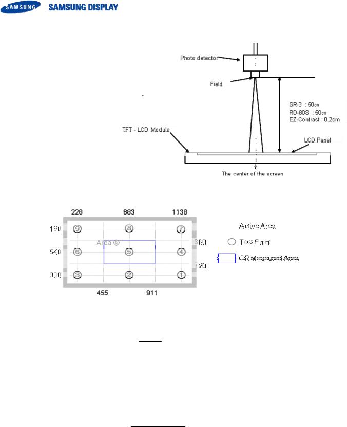
Photo detector |
Field |
|
|
SR-3 |
2°/1° |
RD-80S |
1° |
|
|
- Definition of the test point
Note (1) Definition of contrast ratio (C/R)
: The ratio of gray max (Gmax) & gray min (Gmin) at the center point of the panel The measurement goes in LTY320AN05-A BLU
G max
G min
Gmax : The luminance with all white pixels
Gmin : The luminance with all black pixels
Note (2) Definition of the Brightness uniformity of 9 points (Test pattern : The full white) The measurement shall be executed with the LTY320AN05-A BLU
Buni =100 (B max− B min)
B max
Bmax : The maximum brightness
Bmin : The minimum brightness
MODEL |
LSY320AN02-A |
Doc. No |
|
Page |
7 / 45 |
|
|
|
|
|
|
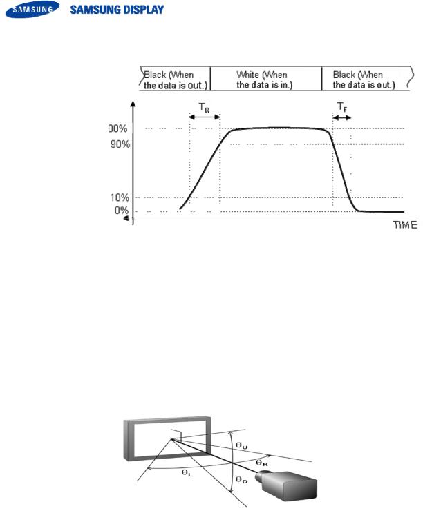
Note (3) Definition of the response time : Sum of Tr, Tf
Display data
The response
Of optical instruments
G-to-G : Average response time between whole gray scale to whole gray scale.
The response time is the value that was measured after it was operated in LTY320AN05-A BLU for one hour.( at room temperature)
Note (4) The definition of luminance of white: The luminance of white at the center point The measurement shall be executed with the LTY320AN05-A BLU.
Note (5) The definition of chromaticity (CIE 1931)
The color coordinate of red, green, blue and white at the center point
The measurement shall be executed with the LTY320AN05-A BLU.
Note (6) Definition of viewing angle
: The range of viewing angle (C/R ≥10)
The measurement shall be executed with the LTY320AN05-A BLU.
Note (7) Definition of transmissivity
: The measurement shall be executed with the D65 Standard Light Source
Note (8) Definition of Gamma
Gamma = log( Xlum / 100) / log(Y / 100)
Xlum = (Z − Bmin ) / (Bmax − Bmin ) ×100
Y: Measurement Level / Z: Measurement Brightness
Bmax: Maximum Brightness / Bmin: Minimum Brightness
MODEL |
LSY320AN02-A |
Doc. No |
|
Page |
8 / 45 |
|
|
|
|
|
|

Note (9) Definition of Simulation with BLU Spectrum
Simulated color Chromaticity
Xsim = Simulated Spectrum X CIE Color Matching Function x
Ysim = Simulated Spectrum X CIE Color Matching Function y
Zsim = Simulated Spectrum X CIE Color Matching Function z
Simulated Spectrum = Panel Transmittance Spectrum X Standard BLU Spectrum(Appendix2)
Note (10) Definition of the Transmissivity uniformity of 9 points
The measurement shall be executed with the D65 Standard Light Source
Tmax : The maximum transmissivity
Tmin : The minimum transmissivity
MODEL |
LSY320AN02-A |
Doc. No |
|
Page |
9 / 45 |
|
|
|
|
|
|
3.Electrical characteristics
3.1TFT LCD Module
The connector for the display data & timing signal should be connected.
Ta = 25°C ± 2 °C
|
|
|
|
|
|
|
|
|
|
|
|
|
|
|
|
|
Item |
|
Symbol |
Min. |
|
Typ. |
|
Max. |
|
|
Unit |
Note |
|
|
|
|
|
|
|
|
|
|
|
|
|
|
|
|
Voltage of Power Supply |
|
VDD |
11 |
|
12 |
|
13 |
|
|
V |
(1) |
|
||
|
|
(a) Black |
|
|
- |
|
325 |
|
- |
|
|
|
|
|
|
|
|
|
|
|
|
|
|
|
|
|
|
|
|
Current |
|
(b) White |
|
IDD |
- |
|
340 |
|
440 |
|
|
|
|
|
|
|
|
|
|
|
|
|
|
||||||
of Power |
|
|
|
|
|
|
|
|
|
|
mA |
(2),(3) |
|
|
|
(c) Mosaic |
|
- |
|
335 |
|
- |
|
|
|
||||
Supply |
|
|
|
|
|
|
|
|
|
|
||||
|
|
|
|
|
|
|
|
|
|
|
|
|
|
|
|
|
(4) Max Pattern |
|
|
- |
|
650 |
|
750 |
|
|
|
|
|
|
|
(V-stripe) |
|
|
|
|
|
|
|
|
|
|||
|
|
|
|
|
|
|
|
|
|
|
|
|
|
|
Vsync Frequency |
|
fV |
47 |
|
60 |
|
63 |
|
|
Hz |
|
|
||
|
|
|
|
|
|
|
|
|
|
|
|
|
||
Hsync Frequency |
|
fH |
45 |
|
48.6 |
|
53 |
|
|
kHz |
|
|
||
|
|
|
|
|
|
|
|
|
|
|
|
|
||
Main Frequency |
|
fDCLK |
65 |
|
80 |
|
86 |
|
|
MHz |
|
|
||
|
Rush Current |
|
IRUSH |
- |
|
- |
|
3 |
|
|
A |
(4) |
|
|
Note (1) The ripple voltage should be controlled fewer than 10% of VDD (Typ.) voltage.
(2) fV=60Hz, fDCLK =80MHz, VDD = 12.0V, DC Current.
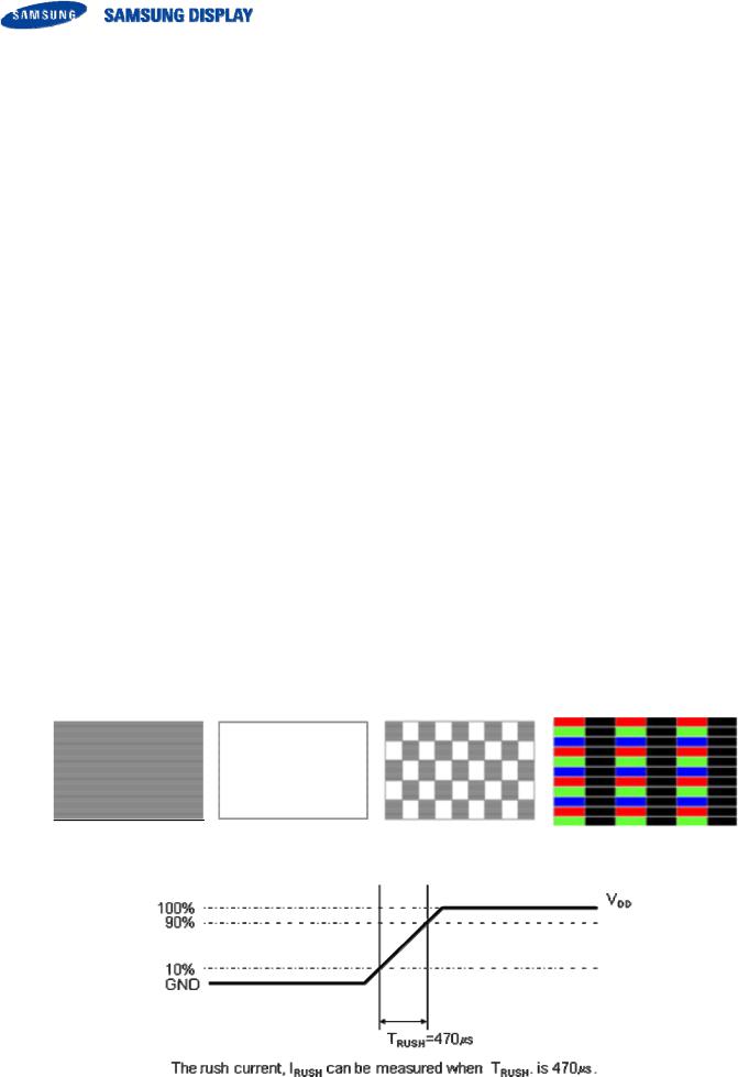
(3) Power dissipation check pattern (LCD Module only)
a) Black pattern |
b) White pattern |
c) Mosaic |
d) Max Pattern(V-Stripe) |
|
|
|
|
(4) Conditions for measurement
|
|
The rush current, IRUSH can be measured during TRUSH |
is 470us |
|
|
|||
|
|
|
|
|
|
|
|
|
|
|
|
|
|
|
|
|
|
MODEL |
LSY320AN02-A |
Doc. No |
|
|
Page |
10 / 45 |
||
|
|
|
|
|
|
|
|
|

4. Block diagram
MODEL |
LSY320AN02-A |
Doc. No |
|
Page |
11 / 45 |
|
|
|
|
|
|

5. The Pin assignment in the input terminal
5.1. Input signal & power |
|
|
Connector : 196260-30041 (P-TWO Industries) |
|||
|
|
|
|
|
|
|
Pin |
Symbol |
|
Description |
Pin |
Symbol |
Description |
|
|
|
|
|
|
|
1 |
NC |
|
NOTE1 |
16 |
GND |
Ground |
|
|
|
|
|
|
|
2 |
SCL_I |
|
I2C SCL |
17 |
LV3_NI |
LV3_NI |
|
|
|
|
|
|
|
3 |
SDA_I |
|
I2C SDA |
18 |
LV3_PI |
LV3_PI |
|
|
|
|
|
|
|
4 |
GND |
|
Ground |
19 |
GND |
Ground |
|
|
|
|
|
|
|
5 |
LV0_NI |
|
LV0_NI |
20 |
NC |
NOTE1 |
|
|
|
|
|
|
|
6 |
LV0_PI |
|
LV0_PI |
21 |
LVDS_SEL |
LVDS_SEL |
|
|
|
|
|
|
|
7 |
GND |
|
Ground |
22 |
WPN(B_INT) |
WPN(B_INT) |
|
|
|
|
|
|
|
8 |
LV1_NI |
|
LV1_NI |
23 |
GND |
Ground |
|
|
|
|
|
|
|
9 |
LV1_PI |
|
LV1_PI |
24 |
GND |
Ground |
|
|
|
|
|
|
|
10 |
GND |
|
Ground |
25 |
NC |
NOTE1 |
|
|
|
|
|
|
|
11 |
LV2_NI |
|
LV2_NI |
26 |
VDD |
Vdd |
|
|
|
|
|
|
|
12 |
LV2_PI |
|
LV2_PI |
27 |
VDD |
Vdd |
|
|
|
|
|
|
|
13 |
GND |
|
Ground + |
28 |
VDD |
Vdd |
|
|
|
|
|
|
|
14 |
LVCLK_NI |
|
LVCLK_NI |
29 |
VDD |
Vdd |
|
|
|
|
|
|
|
15 |
LVCLK_PI |
|
LVCLK_PI |
30 |
VDD |
Vdd |
|
|
|
|
|
|
|
Note (1) No connection: These PINS are used only for the product of SAMSUNG. (DO NOT CONNECT the input device to these pins.)
■ Option Pin Description
These pins are CMOS interface.
Please use within the range of the following restriction. VIH 2.4V(min) / 3.5V(max)
VIL 0.0V(min) / 0.4V(max)) ■SCL : Pull up 22Ω/ 4.7kΩ ■SDA : Pull up 22Ω/ 4.7kΩ
■LVDS_SEL : Pull up - Normal(VESA) Pull down – JEIDA
Note (2) WPN,SCL_I and SDA_I shouldn’t be communicated with I2C device whose output level is 5V
MODEL |
LSY320AN02-A |
Doc. No |
|
Page |
12 / 45 |
|
|
|
|
|
|
Note (3) Pin number which starts from the left side.
▼
130 30
#1 #3030
#1 |
#30 |
|
|
a.Power GND pins should be connected to the LCD’s metal chassis.
b.All power input pins should be connected together.
c.All NC pins should be separated from other signal or power.
Note(4) LVDS OPTION : IF THIS PIN : LOW (GND V)/ NC → JEIDA LVDS FORMAT
OTHERWISE : HIGH (3.3V) → NORMAL NS LVDS FORMAT
MODEL |
LSY320AN02-A |
Doc. No |
|
Page |
13 / 45 |
|
|
|
|
|
|

5.2 LVDS Interface
-LVDS receiver : T-con (merged) ( 8Bit)
-Data format
|
|
LVDS pin |
|
|
JEIDA -DATA |
|
Normal-DATA |
|
|
|
|
|
|||
|
|
|
|
|
|
|
|
|
|
TxIN/RxOUT0 |
|
R2 |
R0 |
||
|
|
|
|
|
|
||
|
|
TxIN/RxOUT1 |
|
R3 |
R1 |
||
|
|
|
|
|
|
||
|
|
TxIN/RxOUT2 |
|
R4 |
R2 |
||
|
|
|
|
|
|
||
TxOUT/RxIN0 |
|
TxIN/RxOUT3 |
|
R5 |
R3 |
||
|
|
|
|
|
|
||
|
|
TxIN/RxOUT4 |
|
R6 |
R4 |
||
|
|
|
|
|
|
||
|
|
TxIN/RxOUT6 |
|
R7 |
R5 |
||
|
|
|
|
|
|
||
|
|
TxIN/RxOUT7 |
|
G2 |
G0 |
||
|
|
|
|
|
|
||
|
|
TxIN/RxOUT8 |
|
G3 |
G1 |
||
|
|
|
|
|
|
||
|
|
TxIN/RxOUT9 |
|
G4 |
G2 |
||
|
|
|
|
|
|
||
|
|
TxIN/RxOUT12 |
|
G5 |
G3 |
||
TxOUT/RxIN1 |
|
|
|
|
|
||
|
TxIN/RxOUT13 |
|
G6 |
G4 |
|||
|
|
|
|
|
|
||
|
|
TxIN/RxOUT14 |
|
G7 |
G5 |
||
|
|
|
|
|
|
||
|
|
TxIN/RxOUT15 |
|
B2 |
B0 |
||
|
|
|
|
|
|
||
|
|
TxIN/RxOUT18 |
|
B3 |
B1 |
||
|
|
|
|
|
|
||
|
|
TxIN/RxOUT19 |
|
B4 |
B2 |
||
|
|
|
|
|
|
||
|
|
TxIN/RxOUT20 |
|
B5 |
B3 |
||
|
|
|
|
|
|
||
|
|
TxIN/RxOUT21 |
|
B6 |
B4 |
||
TxOUT/RxIN2 |
|
|
|
|
|
||
|
TxIN/RxOUT22 |
|
B7 |
B5 |
|||
|
|
|
|
|
|
||
|
|
TxIN/RxOUT24 |
|
HSYNC |
HSYNC |
||
|
|
|
|
|
|
||
|
|
TxIN/RxOUT25 |
|
VSYNC |
VSYNC |
||
|
|
|
|
|
|
||
|
|
TxIN/RxOUT26 |
|
DEN |
DE |
||
|
|
|
|
|
|
||
|
|
TxIN/RxOUT27 |
|
R0 |
R6 |
||
|
|
|
|
|
|
||
|
|
TxIN/RxOUT5 |
|
R1 |
R7 |
||
|
|
|
|
|
|
||
|
|
TxIN/RxOUT10 |
|
G0 |
G6 |
||
|
|
|
|
|
|
||
TxOUT/RxIN3 |
|
TxIN/RxOUT11 |
|
G1 |
G7 |
||
|
|
|
|
|
|
||
|
|
TxIN/RxOUT16 |
|
B0 |
B6 |
||
|
|
|
|
|
|
||
|
|
TxIN/RxOUT17 |
|
B1 |
B7 |
||
|
|
|
|
|
|
||
|
|
TxIN/RxOUT23 |
|
RESERVED |
RESERVED |
||
|
|
|
|
|
|
|
|
MODEL |
LSY320AN02-A |
Doc. No |
|
Page |
14 / 45 |
|
|
|
|
|
|
 Loading...