


 Loading...
Rev. 1.0, Feb. 2019
M393AAG40M3B
288pin Registered DIMM based on 16Gb M-die
78FBGA with Lead-Free & Halogen-Free (RoHS compliant)
datasheet
SAMSUNG ELECTRONICS RESERVES THE RIGHT TO CHANGE PRODUCTS, INFORMATION AND
SPECIFICATIONS WITHOUT NOTICE.
Products and specifications discussed herein are for reference purposes only. All information discussed herein is provided on an "AS IS" basis, without warranties of any kind.
This document and all information discussed herein remain the sole and exclusive property of Samsung Electronics. No license of any patent, copyright, mask work, trademark or any other intellectual property right is granted by one party to the other party under this document, by implication, estoppel or otherwise.
Samsung products are not intended for use in life support, critical care, medical, safety equipment, or similar applications where product failure could result in loss of life or personal or physical harm, or any military or defense application, or any governmental procurement to which special terms or provisions may apply.
For updates or additional information about Samsung products, contact your nearest Samsung office.
All brand names, trademarks and registered trademarks belong to their respective owners.
© 2019 Samsung Electronics Co., Ltd. All rights reserved.
- 1 -

Registered DIMM
datasheet |
Rev. 1.0 |
DDR4 SDRAM |
Revision History
Revision No. |
History |
Draft Date |
Remark |
Editor |
0.0 |
- First version for target specification. |
21st Sep, 2018 |
Target |
T.Y.Lee |
|
|
|
|
J.Y.Bae |
1.0 |
- Final datasheet. |
21st Feb, 2019 |
Final |
T.Y.Lee |
|
- Update IDD table |
|
|
J.Y.Bae |
1. Update IDD and IPP values.
2. Remove symbol IDD5B2, IDD5F3, IDD5F5, IPP5B2, IPP5F3 and IPP5F5.
- Update Speed bins table.
- Add Timings used for IDD, IPP and IDDQ Measurement-Loop Patterns table.
- Update Basic IDD, IPP and IDDQ Measurement Conditions table. 1. Correct typo.
2. Remove IDD4RB/IDDQ4RB/IDD4WB.
3. Add IDD5B2/IPP5B2/IDD5F3/IPP5F3/IDD5F5/IPP5F5 parameters.
- Update DDR4-2933 Speed Bins and Operations table. - Correct CAS latency in Key features.
- 2 -

Registered DIMM
datasheet |
Rev. 1.0 |
DDR4 SDRAM |
Table Of Contents
288pin Registered DIMM based on 16Gb M-die
1. DDR4 REGISTERED DIMM ORDERING INFORMATION .................................................................................................................. |
5 |
|
2. KEY FEATURES .................................................................................................................................................................................. |
5 |
|
3. ADDRESS CONFIGURATION ............................................................................................................................................................. |
5 |
|
4. REGISTERED DIMM PIN CONFIGURATIONS (FRONT SIDE/BACK SIDE)...................................................................................... |
6 |
|
5. PIN DESCRIPTION ............................................................................................................................................................................. |
7 |
|
6. ON DIMM THERMAL SENSOR ........................................................................................................................................................... |
8 |
|
7. INPUT/OUTPUT FUNCTIONAL DESCRIPTION ................................................................................................................................. |
9 |
|
8. REGISTERING CLOCK DRIVER SPECIFICATION ............................................................................................................................ |
11 |
|
8.1 Timing & Capacitance values ......................................................................................................................................................... |
11 |
|
8.2 Clock driver Characteristics ............................................................................................................................................................ |
11 |
|
9. FUNCTION BLOCK DIAGRAM: ........................................................................................................................................................... |
12 |
|
9.1 128GB, 16Gx72 Module ................................................................................................................................................................. |
12 |
|
9.1.1. (PC4-RDIMM Populated as 2 physical ranks / 2 logical ranks of x4 DDR4 SDRAMs) ........................................................... |
12 |
|
10. ABSOLUTE MAXIMUM RATINGS ..................................................................................................................................................... |
15 |
|
11. AC & DC OPERATING CONDITIONS ............................................................................................................................................... |
15 |
|
12. AC & DC INPUT MEASUREMENT LEVELS...................................................................................................................................... |
16 |
|
12.1 |
AC & DC Logic Input Levels for Single-Ended Signals................................................................................................................. |
16 |
12.2 |
AC and DC Input Measurement Levels: VREF Tolerances.......................................................................................................... |
16 |
12.3 |
AC and DC Logic Input Levels for Differential Signals ................................................................................................................. |
17 |
12.3.1. Differential Signals Definition ................................................................................................................................................ |
17 |
|
12.3.2. Differential Swing Requirements for Clock (CK_t - CK_c) .................................................................................................... |
17 |
|
12.3.3. Single-ended Requirements for Differential Signals ............................................................................................................. |
18 |
|
12.3.4. Address, Command and Control Overshoot and Undershoot specifications........................................................................ |
19 |
|
12.3.5. Clock Overshoot and Undershoot Specifications.................................................................................................................. |
20 |
|
12.3.6. Data, Strobe and Mask Overshoot and Undershoot Specifications...................................................................................... |
21 |
|
12.4 |
Slew Rate Definitions.................................................................................................................................................................... |
22 |
12.4.1. Slew Rate Definitions for Differential Input Signals (CK) ...................................................................................................... |
22 |
|
12.4.2. Slew Rate Definition for Single-ended Input Signals (CMD/ADD) ........................................................................................ |
23 |
|
12.5 |
Differential Input Cross Point Voltage........................................................................................................................................... |
24 |
12.6 |
CMOS rail to rail Input Levels ....................................................................................................................................................... |
25 |
12.6.1. CMOS rail to rail Input Levels for RESET_n ......................................................................................................................... |
25 |
|
12.7 |
AC and DC Logic Input Levels for DQS Signals........................................................................................................................... |
26 |
12.7.1. Differential signal definition ................................................................................................................................................... |
26 |
|
12.7.2. Differential swing requirements for DQS (DQS_t - DQS_c).................................................................................................. |
26 |
|
12.7.3. Peak voltage calculation method .......................................................................................................................................... |
27 |
|
12.7.4. Differential Input Cross Point Voltage ................................................................................................................................... |
28 |
|
12.7.5. Differential Input Slew Rate Definition .................................................................................................................................. |
29 |
|
13. AC AND DC OUTPUT MEASUREMENT LEVELS ............................................................................................................................ |
30 |
|
13.1 |
Output Driver DC Electrical Characteristics.................................................................................................................................. |
30 |
13.1.1. Output Driver Temperature and Voltage Sensitivity.............................................................................................................. |
32 |
|
13.1.2. Alert_n output Drive Characteristic ....................................................................................................................................... |
32 |
|
13.1.3. Output Driver Characteristic of Connectivity Test (CT) Mode............................................................................................... |
33 |
|
13.2 |
Single-ended AC & DC Output Levels.......................................................................................................................................... |
34 |
13.3 |
Differential AC & DC Output Levels.............................................................................................................................................. |
34 |
13.4 |
Single-ended Output Slew Rate ................................................................................................................................................... |
35 |
13.5 |
Differential Output Slew Rate ....................................................................................................................................................... |
36 |
13.6 |
Single-ended AC & DC Output Levels of Connectivity Test Mode ............................................................................................... |
37 |
13.7 |
Test Load for Connectivity Test Mode Timing .............................................................................................................................. |
38 |
14. IDD AND IDDQ SPECIFICATION PARAMETERS AND TEST CONDITIONS .................................................................................. |
39 |
|
14.1 |
IDD, IPP and IDDQ Measurement Conditions.............................................................................................................................. |
39 |
15. DIMM IDD SPECIFICATION DEFINITION......................................................................................................................................... |
42 |
|
16. IDD TABLE ......................................................................................................................................................................................... |
55 |
|
17. INPUT/OUTPUT CAPACITANCE ...................................................................................................................................................... |
57 |
|
18. ELECTRICAL CHARACTERISTICS & AC TIMINGS FOR DDR4-1600-3DS TO DDR4-2933-3DS .................................................. |
58 |
|
18.1 |
Refresh parameters ...................................................................................................................................................................... |
58 |
18.2 |
Speed Bins and CL, tRCD, tRP, tRC and tRAS for corresponding bin......................................................................................... |
60 |
18.3 |
Speed Bin Table Note................................................................................................................................................................... |
65 |
19. ELECTRICAL CHARACTERISTICS & AC TIMING ........................................................................................................................... |
66 |
|
19.1 |
Reference Load for AC Timing and Output Slew Rate ................................................................................................................. |
66 |
|
- 3 - |
|

Registered DIMM
datasheet |
Rev. 1.0 |
DDR4 SDRAM |
19.2 tREFI............................................................................................................................................................................................. |
66 |
|
19.3 |
Clock Specification ....................................................................................................................................................................... |
67 |
19.3.1. Definition for tCK(abs)........................................................................................................................................................... |
67 |
|
19.3.2. Definition for tCK(avg)........................................................................................................................................................... |
67 |
|
19.3.3. Definition for tCH(avg) and tCL(avg).................................................................................................................................... |
67 |
|
19.3.4. Definition for tERR(nper)....................................................................................................................................................... |
67 |
|
20. TIMING PARAMETERS BY SPEED GRADE .................................................................................................................................... |
68 |
|
20.1 |
Rounding Algorithms ................................................................................................................................................................... |
74 |
20.2 |
The DQ input receiver compliance mask for voltage and timing .................................................................................................. |
75 |
20.3 |
Command, Control, and Address Setup, Hold, and Derating ....................................................................................................... |
79 |
20.4 |
DDR4 Function Matrix .................................................................................................................................................................. |
81 |
21. PHYSICAL DIMENSIONS .................................................................................................................................................................. |
83 |
|
21.1 |
8Gbx4(3DS 2H) based 16Gx72 Module (M393AAG40M3B)........................................................................................................ |
83 |
21.1.1. x72 DIMM, populated as 2 physical ranks / 2 logical ranks of x4 DDR4 SDRAMs............................................................... |
83 |
|
21.1.2. .............................................................................................................................................................................................. |
83 |
|
22. PRODUCT REGULATORY COMPLIANCE ....................................................................................................................................... |
84 |
|
22.1 |
Product Regulatory Compliance And Certifications...................................................................................................................... |
84 |
- 4 -

Registered DIMM
datasheet |
Rev. 1.0 |
DDR4 SDRAM |
1. DDR4 REGISTERED DIMM ORDERING INFORMATION
[Table 1] Ordering Information Table
Part Number |
Density |
Organization |
Component Composition |
Number of Rank |
Height |
M393AAG40M3B-CYF |
128GB |
16Gx72 |
3DS 2H 8Gx4 (K4ABG45WM-3C##)*36 |
4 |
31.25mm |
(2 physical ranks / 2 logical ranks) |
|||||
|
|
|
|
|
|
NOTE :
1)"##" - YF
2)RB(2133Mbps 17-15-15)/TC(2400Mbps 19-17-17) /WD(2666Mbps 22-19-19)
- DDR4-2666(22-19-19) is backward compatible to DDR4-2400(19-17-17) and DDR4-2133(17-15-15) YF(2933Mbps 24-21-21)
- DDR4-2933(24-21-21) is backward compatible to DDR4-2666(22-19-19), DDR4-2400(19-17-17) and DDR4-2133(17-15-15).
2. KEY FEATURES
[Table 2] Speed bins
Speed |
DDR4-2133 |
DDR4-2400 |
DDR4-2666 |
DDR-2933 |
Unit |
|
17-15-15 |
19-17-17 |
22-19-19 |
24-21-21 |
|||
|
|
|||||
tCK |
0.937 |
0.833 |
0.750 |
0.682 |
ns |
|
|
|
|
|
|
|
|
CAS Latency |
17 |
19 |
22 |
24 |
nCK |
|
|
|
|
|
|
|
|
tRCD |
14.06 |
14.16 |
14.25 |
14.32 |
ns |
|
|
|
|
|
|
|
|
tRP |
14.06 |
14.16 |
14.25 |
14.32 |
ns |
|
|
|
|
|
|
|
|
tRAS |
33 |
32 |
32 |
32 |
ns |
|
|
|
|
|
|
|
|
tRC |
47.06 |
46.16 |
46.25 |
46.32 |
ns |
|
|
|
|
|
|
|
•JEDEC standard 1.2V ± 0.06V Power Supply
•VDDQ = 1.2V ± 0.06V
•800 MHz fCK for 1600Mb/sec/pin,933 MHz fCK for 1866Mb/sec/pin, 1067MHz fCK for 2133Mb/sec/pin, 1200MHz fCK for 2400Mb/sec/pin,1333MHz fCK for 2666Mb/sec/pin, 1467MHz fCK for 2933Mb/sec/pin.
•16 Banks (4 Bank Groups)
•Programmable CAS Latency: 11,12,13,14,15,16,17,18,20,22,24,25
•Programmable Additive Latency (Posted CAS): CL - 2 or CL - 1 clock
•Programmable CAS Write Latency (CWL) = 9,11 (DDR4-1600), 10,11,12 (DDR4-1866), 11,14 (DDR4-2133), 12,16 (DDR4-2400), 14,18 (DDR42666) and 16, 20 (DDR4-2933)
•Burst Length: 8, 4 with tCCD = 4 which does not allow seamless read or write [either On the fly using A12 or MRS]
•Bi-directional Differential Data Strobe
•On Die Termination using ODT pin
•Average Refresh Period 7.8us at lower then TCASE 85 C, 3.9us at 85 C < TCASE 95 C
•Asynchronous Reset
3. ADDRESS CONFIGURATION
Organization |
Row Address |
Column Address |
Bank Address |
Auto Precharge |
8Gx4(32Gb 3DS 2H) based Module |
A0-A17 |
A0-A9 |
BA0-BA1 |
A10/AP |
|
|
|
|
|
- 5 -

Registered DIMM
datasheet |
Rev. 1.0 |
DDR4 SDRAM |
4. REGISTERED DIMM PIN CONFIGURATIONS (FRONT SIDE/BACK SIDE)
Pin |
Front |
Pin |
Back |
Pin |
Front |
|
Pin |
Back |
Pin |
Front |
Pin |
Back |
Pin |
Front |
Pin |
Back |
1 |
12V3),NC |
145 |
12V3),NC |
40 |
TDQS12_t, |
|
184 |
VSS |
78 |
EVENT_n |
222 |
PARITY |
117 |
DQ52 |
261 |
VSS |
DQS12_t |
|
|||||||||||||||
|
|
|
|
|
|
|
|
|
|
|
|
|
|
|
|
|
|
|
|
|
|
|
|
|
|
|
|
|
|
|
|
|
|
2 |
VSS |
146 |
VREFCA |
41 |
TDQS12_c, |
|
185 |
DQS3_c |
79 |
A0 |
223 |
VDD |
118 |
VSS |
262 |
DQ53 |
DQS12_c |
|
|||||||||||||||
|
|
|
|
|
|
|
|
|
|
|
|
|
|
|
|
|
|
|
|
|
|
|
|
|
|
|
|
|
|
|
|
|
|
3 |
DQ4 |
147 |
VSS |
42 |
VSS |
|
186 |
DQS3_t |
80 |
VDD |
224 |
BA1 |
119 |
DQ48 |
263 |
VSS |
|
|
|
|
|
|
|
|
|
|
|
|
|
|
|
|
|
4 |
VSS |
148 |
DQ5 |
43 |
DQ30 |
|
187 |
VSS |
81 |
BA0 |
225 |
A10/AP |
120 |
VSS |
264 |
DQ49 |
|
|
|
|
|
|
|
|
|
|
|
|
|
|
|
|
|
5 |
DQ0 |
149 |
VSS |
44 |
VSS |
|
188 |
DQ31 |
82 |
RAS_n/A16 |
226 |
VDD |
121 |
TDQS15_t, |
265 |
VSS |
|
DQS15_t |
|||||||||||||||
|
|
|
|
|
|
|
|
|
|
|
|
|
|
|
|
|
|
|
|
|
|
|
|
|
|
|
|
|
|
|
|
|
|
6 |
VSS |
150 |
DQ1 |
45 |
DQ26 |
|
189 |
VSS |
83 |
VDD |
227 |
RFU |
122 |
TDQS15_c, |
266 |
DQS6_c |
|
DQS15_c |
|||||||||||||||
|
|
|
|
|
|
|
|
|
|
|
|
|
|
|
|
|
7 |
TDQS9_t, |
151 |
VSS |
46 |
VSS |
|
190 |
DQ27 |
84 |
S0_n |
228 |
WE_n/A14 |
123 |
VSS |
267 |
DQS6_t |
DQS9_t |
|
|||||||||||||||
|
|
|
|
|
|
|
|
|
|
|
|
|
|
|
|
|
|
|
|
|
|
|
|
|
|
|
|
|
|
|
|
|
|
8 |
TDQS9_c, |
152 |
DQS0_c |
47 |
CB4 |
|
191 |
VSS |
85 |
VDD |
229 |
VDD |
124 |
DQ54 |
268 |
VSS |
DQS9_c |
|
|||||||||||||||
|
|
|
|
|
|
|
|
|
|
|
|
|
|
|
|
|
|
|
|
|
|
|
|
|
|
|
|
|
|
|
|
|
|
9 |
VSS |
153 |
DQS0_t |
48 |
VSS |
|
192 |
CB5 |
86 |
CAS_n/A15 |
230 |
NC |
125 |
VSS |
269 |
DQ55 |
|
|
|
|
|
|
|
|
|
|
|
|
|
|
|
|
|
10 |
DQ6 |
154 |
VSS |
49 |
CB0 |
|
193 |
VSS |
87 |
ODT0 |
231 |
VDD |
126 |
DQ50 |
270 |
VSS |
|
|
|
|
|
|
|
|
|
|
|
|
|
|
|
|
|
11 |
VSS |
155 |
DQ7 |
50 |
VSS |
|
194 |
CB1 |
88 |
VDD |
232 |
A13 |
127 |
VSS |
271 |
DQ51 |
|
|
|
|
|
|
|
|
|
|
|
|
|
|
|
|
|
12 |
DQ2 |
156 |
VSS |
51 |
TDQS17_t, |
|
195 |
VSS |
89 |
S1_n |
233 |
VDD |
128 |
DQ60 |
272 |
VSS |
DQS17_t |
|
|||||||||||||||
|
|
|
|
|
|
|
|
|
|
|
|
|
|
|
|
|
|
|
|
|
|
|
|
|
|
|
|
|
|
|
|
|
|
13 |
VSS |
157 |
DQ3 |
52 |
TDQS17_c, |
|
196 |
DQS8_c |
90 |
VDD |
234 |
A17 |
129 |
VSS |
273 |
DQ61 |
DQS17_c |
|
|||||||||||||||
|
|
|
|
|
|
|
|
|
|
|
|
|
|
|
|
|
|
|
|
|
|
|
|
|
|
|
|
|
|
|
|
|
|
14 |
DQ12 |
158 |
VSS |
53 |
VSS |
|
197 |
DQS8_t |
91 |
ODT1 |
235 |
NC,C2 |
130 |
DQ56 |
274 |
VSS |
|
|
|
|
|
|
|
|
|
|
|
|
|
|
|
|
|
15 |
VSS |
159 |
DQ13 |
54 |
CB6 |
|
198 |
VSS |
92 |
VDD |
236 |
VDD |
131 |
VSS |
275 |
DQ57 |
|
|
|
|
|
|
|
|
|
|
|
|
|
|
|
|
|
16 |
DQ8 |
160 |
VSS |
55 |
VSS |
|
199 |
CB7 |
93 |
C0,CS2_n,NC |
237 |
NC,CS3_c,C1 |
132 |
TDQS16_t, |
276 |
VSS |
|
DQS16_t |
|||||||||||||||
|
|
|
|
|
|
|
|
|
|
|
|
|
|
|
|
|
|
|
|
|
|
|
|
|
|
|
|
|
|
|
|
|
|
17 |
VSS |
161 |
DQ9 |
56 |
CB2 |
|
200 |
VSS |
94 |
VSS |
238 |
SA2 |
133 |
TDQS16_c, |
277 |
DQS7_c |
|
DQS16_c |
|||||||||||||||
|
|
|
|
|
|
|
|
|
|
|
|
|
|
|
|
|
|
|
|
|
|
|
|
|
|
|
|
|
|
|
|
|
|
18 |
TDQS10_t, |
162 |
VSS |
57 |
VSS |
|
201 |
CB3 |
95 |
DQ36 |
239 |
VSS |
134 |
VSS |
278 |
DQS7_t |
DQS10_t |
|
|||||||||||||||
|
|
|
|
|
|
|
|
|
|
|
|
|
|
|
|
|
|
|
|
|
|
|
|
|
|
|
|
|
|
|
|
|
|
19 |
TDQS10_c, |
163 |
DQS1_c |
58 |
RESET_n |
|
202 |
VSS |
96 |
VSS |
240 |
DQ37 |
135 |
DQ62 |
279 |
VSS |
DQS10_c |
|
|||||||||||||||
|
|
|
|
|
|
|
|
|
|
|
|
|
|
|
|
|
|
|
|
|
|
|
|
|
|
|
|
|
|
|
|
|
|
20 |
VSS |
164 |
DQS1_t |
59 |
VDD |
|
203 |
CKE1 |
97 |
DQ32 |
241 |
VSS |
136 |
VSS |
280 |
DQ63 |
|
|
|
|
|
|
|
|
|
|
|
|
|
|
|
|
|
21 |
DQ14 |
165 |
VSS |
60 |
CKE0 |
|
204 |
VDD |
98 |
VSS |
242 |
DQ33 |
137 |
DQ58 |
281 |
VSS |
|
|
|
|
|
|
|
|
|
|
|
|
|
|
|
|
|
22 |
VSS |
166 |
DQ15 |
61 |
VDD |
|
205 |
RFU |
99 |
TDQS13_t, |
243 |
VSS |
138 |
VSS |
282 |
DQ59 |
|
DQS13_t |
|||||||||||||||
|
|
|
|
|
|
|
|
|
|
|
|
|
|
|
|
|
|
|
|
|
|
|
|
|
|
|
|
|
|
|
|
|
|
23 |
DQ10 |
167 |
VSS |
62 |
ACT_n |
|
206 |
VDD |
100 |
TDQS13_c, |
244 |
DQS4_c |
139 |
SA0 |
283 |
VSS |
|
DQS13_c |
|||||||||||||||
|
|
|
|
|
|
|
|
|
|
|
|
|
|
|
|
|
|
|
|
|
|
|
|
|
|
|
|
|
|
|
|
|
|
24 |
VSS |
168 |
DQ11 |
63 |
BG0 |
|
207 |
BG1 |
101 |
VSS |
245 |
DQS4_t |
140 |
SA1 |
284 |
VDDSPD |
|
|
|
|
|
|
|
|
|
|
|
|
|
|
|
|
|
25 |
DQ20 |
169 |
VSS |
64 |
VDD |
|
208 |
ALERT_n |
102 |
DQ38 |
246 |
VSS |
141 |
SCL |
285 |
SDA |
|
|
|
|
|
|
|
|
|
|
|
|
|
|
|
|
|
26 |
VSS |
170 |
DQ21 |
65 |
A12/BC_n |
|
209 |
VDD |
103 |
VSS |
247 |
DQ39 |
142 |
VPP |
286 |
VPP |
|
|
|
|
|
|
|
|
|
|
|
|
|
|
|
|
|
27 |
DQ16 |
171 |
VSS |
66 |
A9 |
|
210 |
A11 |
104 |
DQ34 |
248 |
VSS |
143 |
VPP |
287 |
VPP |
|
|
|
|
|
|
|
|
|
|
|
|
|
|
|
|
|
28 |
VSS |
172 |
DQ17 |
67 |
VDD |
|
211 |
A7 |
105 |
VSS |
249 |
DQ35 |
144 |
RFU |
288 |
VPP4) |
29 |
TDQS11_t, |
173 |
VSS |
68 |
A8 |
|
212 |
VDD |
106 |
DQ44 |
250 |
VSS |
|
|
|
|
DQS11_t |
|
|
|
|
|
|||||||||||
|
|
|
|
|
|
|
|
|
|
|
|
|
|
|
|
|
|
|
|
|
|
|
|
|
|
|
|
|
|
|
|
|
|
30 |
TDQS11_c, |
174 |
DQS2_c |
69 |
A6 |
|
213 |
A5 |
107 |
VSS |
251 |
DQ45 |
|
|
|
|
DQS11_c |
|
|
|
|
|
|||||||||||
|
|
|
|
|
|
|
|
|
|
|
|
|
|
|
|
|
|
|
|
|
|
|
|
|
|
|
|
|
|
|
|
|
|
31 |
VSS |
175 |
DQS2_t |
70 |
VDD |
|
214 |
A4 |
108 |
DQ40 |
252 |
VSS |
|
|
|
|
|
|
|
|
|
|
|
|
|
|
|
|
|
|
|
|
|
32 |
DQ22 |
176 |
VSS |
71 |
A3 |
|
215 |
VDD |
109 |
VSS |
253 |
DQ41 |
|
|
|
|
|
|
|
|
|
|
|
|
|
|
|
|
|
|
|
|
|
33 |
VSS |
177 |
DQ23 |
72 |
A1 |
|
216 |
A2 |
110 |
TDQS14_t, |
254 |
VSS |
|
|
|
|
|
DQS14_t |
|
|
|
|
|||||||||||
|
|
|
|
|
|
|
|
|
|
|
|
|
|
|
|
|
|
|
|
|
|
|
|
|
|
|
|
|
|
|
|
|
|
34 |
DQ18 |
178 |
VSS |
73 |
VDD |
|
217 |
VDD |
111 |
TDQS14_c, |
255 |
DQS5_c |
|
|
|
|
|
DQS14_c |
|
|
|
|
|||||||||||
|
|
|
|
|
|
|
|
|
|
|
|
|
|
|
|
|
|
|
|
|
|
|
|
|
|
|
|
|
|
|
|
|
|
35 |
VSS |
179 |
DQ19 |
74 |
CK0_t |
|
218 |
CK1_t |
112 |
VSS |
256 |
DQS5_t |
|
|
|
|
|
|
|
|
|
|
|
|
|
|
|
|
|
|
|
|
|
36 |
DQ28 |
180 |
VSS |
75 |
CK0_c |
|
219 |
CK1_c |
113 |
DQ46 |
257 |
VSS |
|
|
|
|
|
|
|
|
|
|
|
|
|
|
|
|
|
|
|
|
|
37 |
VSS |
181 |
DQ29 |
76 |
VDD |
|
220 |
VDD |
114 |
VSS |
258 |
DQ47 |
|
|
|
|
|
|
|
|
|
|
|
|
|
|
|
|
|
|
|
|
|
38 |
DQ24 |
182 |
VSS |
77 |
VTT |
|
221 |
VTT |
115 |
DQ42 |
259 |
VSS |
|
|
|
|
|
|
|
|
|
|
|
|
|
|
|
|
|
|
|
|
|
39 |
VSS |
183 |
DQ25 |
|
KEY |
|
|
116 |
VSS |
260 |
DQ43 |
|
|
|
|
|
|
|
|
|
|
|
|
|
|
|
|
|
|
|
|
|
|
NOTE:
1)VPP is 2.5V DC
2)Pin 230 is defined as NC for UDIMMs, RDIMMs and LRDIMMs. Pin 230 is defined as SAVE_n for NVDIMMs.
3)Pins 1 and 145 are defined as NC for UDIMMs, RDIMMs and LRDIMMs. Pins 1 and 145 are defined as 12V for Hybrid /NVDIMM
4)The 5th VPP is required on all modules. DIMMs.
- 6 -

Registered DIMM
datasheet |
Rev. 1.0 |
DDR4 SDRAM |
5. PIN DESCRIPTION
Pin Name |
Description |
|
A0-A171) |
Register address input |
|
BA0, BA1 |
Register bank select input |
|
|
|
|
BG0, BG1 |
Register bank group select input |
|
|
|
|
RAS_n2) |
Register row address strobe input |
|
CAS_n3) |
Register column address strobe input |
|
WE_n4) |
Register write enable input |
|
CS0_n, CS1_n, |
DIMM Rank Select Lines input |
|
CS2_n, CS3_n |
||
|
||
|
|
|
CKE0, CKE1 |
Register clock enable lines input |
|
|
|
|
ODT0, ODT1 |
Register on-die termination control lines input |
|
|
|
|
ACT_n |
Register input for activate input |
|
|
|
|
DQ0–DQ63 |
DIMM memory data bus |
|
|
|
|
CB0–CB7 |
DIMM ECC check bits |
|
|
|
|
DQS0_t-DQS17_t |
Data Buffer data strobes |
|
|
(positive line of differential pair) |
|
DQS0_c- |
Data Buffer data strobes |
|
DQS17_c |
(negative line of differential pair) |
|
|
|
|
CK0_t, CK1_t |
Register clock input |
|
(positive line of differential pair) |
||
|
||
|
|
|
CK0_c, CK1_c |
Register clocks input |
|
(negative line of differential pair) |
||
|
||
|
|
NOTE :
1)Address A17 is only valid for 16 Gb x4 based SDRAMs.
2)RAS_n is a multiplexed function with A16.
3)CAS_n is a multiplexed function with A15.
4)WE_n is a multiplexed function with A14.
Pin Name |
Description |
SCL |
I2C serial bus clock for SPD/TS and register |
|
|
SDA |
I2C serial bus data line for SPD/TS and register |
|
|
SA0-SA2 |
I2C slave address select for SPD/TS and register |
|
|
PAR |
Register parity input |
|
|
VDD |
SDRAM core power supply |
|
|
VPP |
SDRAM activating power supply |
|
|
VREFCA |
SDRAM command/address reference supply |
|
|
VSS |
Power supply return (ground) |
|
|
VDDSPD |
Serial SPD/TS positive power supply |
|
|
ALERT_n |
Register ALERT_n output |
|
|
RESET_n |
Set Register and SDRAMs to a Known State |
|
|
EVENT_n |
SPD signals a thermal event has occurred |
|
|
VTT |
SDRAM I/O termination supply |
|
|
RFU |
Reserved for future use |
|
|
- 7 -

Registered DIMM
datasheet |
Rev. 1.0 |
DDR4 SDRAM |
6. ON DIMM THERMAL SENSOR
SA2
SA1 |
|
|
|
|
|
SA0 |
|
|
1K |
|
|
|
|
|
|
|
|
SA0 |
SA1 |
SA2 |
SA0 |
SA1 |
SA2 |
|
SCL |
|
|
SCL |
|
|
|
|
|
SCL |
|
|
|
|
||||
|
|
|
|
|
|
|
|
|
|
|
|
|||||||
|
SDA |
|
|
SDA |
|
|
|
|
|
SDA |
|
|
|
|
||||
|
|
|
|
|
|
|
|
|
|
|
|
|||||||
|
|
|
|
EVENT_n |
|
EVENT_n |
|
|
|
ZQCAL |
|
|
VSS |
|
|
|||
|
|
|
|
|
|
|
|
|
|
|
|
|||||||
|
|
|
|
|
|
|
|
|
|
|
|
|
|
|
|
|
||
|
|
|
|
Serial PD with |
|
|
|
Register |
|
|
|
|
||||||
|
|
|
|
Thermal sensor |
|
|
|
|
|
|
|
|||||||
|
|
|
|
|
|
|
|
|
|
|
|
|
|
|||||
NOTE : |
|
|
|
|
|
|
|
|
|
|
|
|
|
|
|
|
|
|
1) All Samsung RDIMM support Thermal sensor on DIMM |
|
|
|
|
|
|
|
|
|
|
|
|
|
|
|
|||
[ Table 3 ] Temperature Sensor Characteristics |
|
|
|
|
|
|
|
|
|
|
|
|
|
|
|
|||
|
|
|
|
|
|
|
|
|
|
|
|
|
|
|
|
|
|
|
Grade |
Range |
|
|
|
|
|
Temperature Sensor Accuracy |
Units |
NOTE |
|||||||||
|
|
|
|
Min. |
|
|
|
Typ. |
|
Max. |
||||||||
|
|
|
|
|
|
|
|
|
|
|
|
|
|
|||||
|
75 < Ta < 95 |
|
- |
|
|
|
+/- 0.5 |
|
+/- 1.0 |
|
- |
|||||||
B |
|
|
|
|
|
|
|
|
|
|
|
|
|
|
|
|
C |
|
40 < Ta < 125 |
|
- |
|
|
|
+/- 1.0 |
|
+/- 2.0 |
- |
|||||||||
|
|
|
|
|
|
|
|
|
|
|
|
|
|
|
|
|
|
|
|
-20 < Ta < 125 |
|
- |
|
|
|
+/- 2.0 |
|
+/- 3.0 |
|
- |
|||||||
|
|
|
|
|
|
|
|
|
|
|
|
|
|
|
|
|
|
|
|
Resolution |
|
|
|
|
|
0.25 |
|
|
|
|
C /LSB |
- |
|||||
|
|
|
|
|
|
|
|
|
|
|
|
|
|
|
|
|
|
|
- 8 -

Registered DIMM
datasheet |
Rev. 1.0 |
DDR4 SDRAM |
7. INPUT/OUTPUT FUNCTIONAL DESCRIPTION
[ Table 4 ] Input/Output Function Description
Symbol |
Type |
Function |
|
CK_t, CK_c |
Input |
Clock: CK_t and CK_c are differential clock inputs. All address and control input signals are sampled on the crossing |
|
of the positive edge of CK_t and negative edge of CK_c. |
|||
|
|
||
|
|
|
|
|
|
Clock Enable: CKE HIGH activates and CKE LOW deactivates, internal clock signals and device input buffers and |
|
|
|
output drivers. Taking CKE LOW provides Precharge Power-Down and Self-Refresh operation (all banks idle), or |
|
CKE, (CKE1) |
Input |
Active Power-Down (row Active in any bank). CKE is synchronous for Self-Refresh exit. After VREFCA and Internal |
|
DQ Vref have become stable during the power on and initialization sequence, they must be maintained during all |
|||
|
|
operations (including Self-Refresh). CKE must be maintained high throughout read and write accesses. Input buffers, |
|
|
|
excluding CK_t, CK_c, ODT and CKE are disabled during power-down. Input buffers, excluding CKE, are disabled |
|
|
|
during Self-Refresh. |
|
|
|
|
|
CS_n, (CS1_n) |
Input |
Chip Select: All commands are masked when CS_n is registered HIGH. CS_n provides for external Rank selection on |
|
systems with multiple Ranks. CS_n is considered part of the command code. |
|||
|
|
||
|
|
|
|
C0, C1, C2 |
Input |
Chip ID : Chip ID is only used for 3DS for 2,4,8 high stack via TSV to select each slice of stacked component. Chip ID |
|
is considered part of the command code. |
|||
|
|
||
|
|
|
|
|
|
On Die Termination: ODT (registered HIGH) enables RTT_NOM termination resistance internal to the DDR4 SDRAM. |
|
ODT, (ODT1) |
Input |
When enabled, ODT is only applied to each DQ, DQS_t, DQS_c and DM_n/DBI_n/TDQS_t, NU/TDQS_c (When |
|
TDQS is enabled via Mode Register A11=1 in MR1) signal for x8 configurations. For x16 configuration ODT is applied |
|||
|
|
to each DQ, DQSU_t, DQSU_c, DQSL_t, DQSL_c, DMU_n, and DML_n signal. The ODT pin will be ignored if MR1 is |
|
|
|
programmed to disable RTT_NOM. |
|
|
|
|
|
ACT_n |
Input |
Activation Command Input : ACT_n defines the Activation command being entered along with CS_n. The input into |
|
RAS_n/A16, CAS_n/A15 and WE_n/A14 will be considered as Row Address A16, A15 and A14 |
|||
|
|
||
|
|
|
|
RAS_n/A16 |
|
Command Inputs: RAS_n/A16, CAS_n/A15 and WE_n/A14 (along with CS_n) define the command being entered. |
|
Input |
Those pins have multi function. For example, for activation with ACT_n Low, these are Addresses like A16, A15 and |
||
CAS_n/A15 |
|||
A14 but for non-activation command with ACT_n High, these are Command pins for Read, Write and other command |
|||
WE_n/A14 |
|
||
|
defined in command truth table |
||
|
|
||
|
|
|
|
|
|
Input Data Mask and Data Bus Inversion: DM_n is an input mask signal for write data. Input data is masked when |
|
DM_n/DBI_n/ |
|
DM_n is sampled LOW coincident with that input data during a Write access. DM_n is sampled on both edges of |
|
TDQS_t, (DMU_n/ |
Input/Output |
DQS. DM is muxed with DBI function by Mode Register A10,A11,A12 setting in MR5. For x8 device, the function of |
|
DBIU_n), (DML_n/ |
|
DM or TDQS is enabled by Mode Register A11 setting in MR1. DBI_n is an input/output identifing whether to store/ |
|
DBIL_n) |
|
output the true or inverted data. If DBI_n is LOW, the data will be stored/output after inversion inside the DDR4 |
|
|
|
SDRAM and not inverted if DBI_n is HIGH. TDQS is only supported in X8. |
|
|
|
|
|
BG0 - BG1 |
Input |
Bank Group Inputs: BG0 - BG1 define to which bank group an Active, Read, Write or Precharge command is being |
|
applied. BG0 also determines which mode register is to be accessed during a MRS cycle. X4/8 have BG0 and BG1 |
|||
|
|
but X16 has only BG0. |
|
|
|
|
|
BA0 - BA1 |
Input |
Bank Address Inputs: BA0 - BA1 define to which bank an Active, Read, Write or Precharge command is being applied. |
|
Bank address also determines which mode register is to be accessed during a MRS cycle. |
|||
|
|
||
|
|
|
|
|
|
Address Inputs: Provide the row address for ACTIVATE Commands and the column address for Read/Write |
|
A0 - A17 |
Input |
commands to select one location out of the memory array in the respective bank. A10/AP, A12/BC_n, RAS_n/A16, |
|
CAS_n/A15 and WE_n/A14 have additional functions. See other rows. The address inputs also provide the op-code |
|||
|
|
||
|
|
during Mode Register Set commands. A17 is only defined for the x4 configuration. |
|
|
|
|
|
|
|
Auto-precharge: A10 is sampled during Read/Write commands to determine whether Autoprecharge should be |
|
A10 / AP |
Input |
performed to the accessed bank after the Read/Write operation. (HIGH: Autoprecharge; LOW: no Autoprecharge). |
|
A10 is sampled during a Precharge command to determine whether the Precharge applies to one bank (A10 LOW) or |
|||
|
|
||
|
|
all banks (A10 HIGH). If only one bank is to be precharged, the bank is selected by bank addresses. |
|
|
|
|
|
A12 / BC_n |
Input |
Burst Chop: A12/BC_n is sampled during Read and Write commands to determine if burst chop (on-the-fly) will be |
|
performed. (HIGH, no burst chop; LOW: burst chopped). See command truth table for details. |
|||
|
|
||
|
|
|
|
RESET_n |
Input |
Active Low Asynchronous Reset: Reset is active when RESET_n is LOW, and inactive when RESET_n is HIGH. |
|
RESET_n must be HIGH during normal operation. RESET_n is a CMOS rail to rail signal with DC high and low at 80% |
|||
|
|
and 20% of VDD. |
|
|
|
|
|
|
|
Data Input/ Output: Bi-directional data bus. If CRC is enabled via Mode register then CRC code is added at the end of |
|
DQ |
Input/ |
Data Burst. Any DQ from DQ0-DQ3 may indicate the internal Vref level during test via Mode Register Setting MR4 |
|
Output |
A4=High. During this mode, RTT value should be set to Hi-Z. Refer to vendor specific data sheets to determine which |
||
|
|||
|
|
DQ is used. |
|
|
|
|
- 9 -

Registered DIMM
datasheet |
Rev. 1.0 |
DDR4 SDRAM |
[ Table 4 ] Input/Output Function Description
Symbol |
Type |
Function |
|
DQS_t, DQS_c, |
|
Data Strobe: output with read data, input with write data. Edge-aligned with read data, centered in write data. For the |
|
Input/ |
x16, DQSL corresponds to the data on DQL0-DQL7; DQSU corresponds to the data on DQU0-DQU7. The data strobe |
||
DQSU_t, DQSU_c, |
DQS_t, DQSL_t and DQSU_t are paired with differential signals DQS_c, DQSL_c, and DQSU_c, respectively, to |
||
Output |
|||
DQSL_t, DQSL_c |
provide differential pair signaling to the system during reads and writes. DDR4 SDRAM supports differential data |
||
|
|||
|
|
strobe only and does not support single-ended. |
|
|
|
|
|
|
|
Termination Data Strobe: TDQS_t/TDQS_c is applicable for x8 DRAMs only. When enabled via Mode Register A11 = |
|
|
|
1 in MR1, the DRAM will enable the same termination resistance function on TDQS_t/TDQS_c that is applied to |
|
TDQS_t, TDQS_c |
Output |
DQS_t/DQS_c. When disabled via mode register A11 = 0 in MR1, DM/DBI/TDQS will provide the data mask function |
|
|
|
or Data Bus Inversion depending on MR5; A11,12,10and TDQS_c is not used. x4/x16 DRAMs must disable the TDQS |
|
|
|
function via mode register A11 = 0 in MR1. |
|
|
|
|
|
|
|
Command and Address Parity Input: DDR4 Supports Even Parity check in DRAM with MR setting. Once it’s enabled |
|
PAR |
Input |
via Register in MR5, then DRAM calculates Parity with ACT_n, RAS_n/A16, CAS_n/A15, WE_n/A14, BG0-BG1, BA0- |
|
BA1, A17-A0 and C0-C2 (3DS devices). Command and address inputs shall have parity check performed when |
|||
|
|
||
|
|
commands are latched via the rising edge of CK_t and when CS_n is low. |
|
|
|
|
|
|
|
Alert : It has multi functions such as CRC error flag, Command and Address Parity error flag as Output signal. If there |
|
|
|
is error in CRC, then ALERT_n goes LOW for the period time interval and goes back HIGH. If there is error in |
|
ALERT_n |
Output/ |
Command Address Parity Check, then ALERT_n goes LOW for relatively long period until on going DRAM internal |
|
Input |
recovery transaction is complete. During Connectivity Test mode this pin works as input. |
||
|
|||
|
|
Using this signal or not is dependent on system. In case of not connected as Signal, ALERT_n Pin must be bounded |
|
|
|
to VDD on board. |
|
|
|
|
|
|
|
Connectivity Test Mode Enable : Required on X16 devices and optional input on x4/x8 with densities equal to or |
|
TEN |
Input |
greater than 8Gb.HIGH in this pin will enable Connectivity Test Mode operation along with other pins. It is a CMOS rail |
|
to rail signal with AC high and low at 80% and 20% of VDD. Using this signal or not is dependent on System. This pin |
|||
|
|
||
|
|
may be DRAM internally pulled low through a weak pull-down resistor to VSS. |
|
|
|
|
|
NC |
|
No Connect: No internal electrical connection is present |
|
|
|
|
|
VDDQ |
Supply |
DQ Power Supply: 1.2V +/- 0.06V |
|
|
|
|
|
VSSQ |
Supply |
DQ Ground |
|
|
|
|
|
VDD |
Supply |
Power Supply: 1.2V ± 0.06V |
|
|
|
|
|
VSS |
Supply |
Ground |
|
|
|
|
|
VPP |
Supply |
DRAM Activating Power Supply: 2.5V (2.375V min, 2.75V max) |
|
|
|
|
|
VREFCA |
Supply |
Reference voltage for CA |
|
|
|
|
|
ZQ |
Supply |
Reference Pin for ZQ calibration |
|
|
|
|
NOTE:
1) Input only pins (BG0-BG1, BA0-BA1, A0-A17, ACT_n, RAS_n/A16, CAS_n/A15, WE_n/A14, CS_n, CKE, ODT and RESET_n) do not supply termination.
- 10 -
Registered DIMM
datasheet |
Rev. 1.0 |
DDR4 SDRAM |
8. REGISTERING CLOCK DRIVER SPECIFICATION
8.1 Timing & Capacitance values
|
|
|
DDR4- |
DDR4- |
DDR4- |
|
Note |
||||
Symbol |
Parameter |
Conditions |
1600/1866/2133 |
2400/2666 |
2933 |
|
Units |
||||
|
|
|
|
|
|
|
|
|
|
|
s |
|
|
|
Min |
Max |
Min |
Max |
Min |
|
Max |
|
|
|
|
|
|
|
|
||||||
fclock |
Input Clock Frequency |
application frequency |
625 |
1080 |
625 |
1350 |
625 |
|
1620 |
MHz |
|
|
|
|
|
|
|
|
|
|
|
|
|
tCH/tCL |
Pulse duration, CK_t, CK_c |
|
0.4 |
- |
0.4 |
- |
0.4 |
|
- |
tCK |
|
HIGH or LOW |
|
|
|
||||||||
|
|
|
|
|
|
|
|
|
|
|
|
|
|
|
|
|
|
|
|
|
|
|
|
tACT |
Inputs active time4 before |
DCKE0/1 = LOW and |
16 |
- |
16 |
- |
16 |
|
- |
tCK |
|
DRST_n is taken HIGH |
DCS0/1_n = HIGH |
|
|
||||||||
|
|
|
|
|
|
|
|
|
|
||
|
|
|
|
|
|
|
|
|
|
|
|
tPDM |
Propagation delay, single-bit |
|
|
|
|
|
|
|
|
|
|
switching, CK_t/ CK_c to out- |
1.2V Operation |
1 |
1.3 |
1 |
1.3 |
1 |
|
1.3 |
ns |
|
|
|
put |
|
|
|
|
|
|
|
|
|
|
|
|
|
|
|
|
|
|
|
|
|
|
tDIS |
|
Rising edge of Yn_t to |
0.5*tCK + |
|
0.5*tCK + |
|
0.5*tCK + |
|
|
|
|
output disable time |
tQSK1(mi |
- |
tQSK1(mi |
- |
tQSK1(mi |
|
- |
ps |
|
||
output float |
|
|
|||||||||
|
|
n) |
|
n) |
|
n) |
|
|
|
|
|
|
|
|
|
|
|
|
|
|
|||
|
|
|
|
|
|
|
|
|
|
|
|
tEN |
|
Output valid to rising |
0.5*tCK - |
|
0.5*tCK - |
|
0.5*tCK - |
|
|
|
|
output enable time |
tQSK1(m |
- |
tQSK1(m |
- |
tQSK1(m |
|
- |
ps |
|
||
edge of Yn_t |
|
|
|||||||||
|
|
ax) |
|
ax) |
|
ax) |
|
|
|
|
|
|
|
|
|
|
|
|
|
|
|||
|
|
|
|
|
|
|
|
|
|
|
|
CI |
Input capacitance, Data inputs |
|
0.8 |
1.1 |
0.8 |
1.0 |
0.8 |
|
1.0 |
|
1,2 |
CCK |
Input capacitance, CK_t, CK_c |
|
0.8 |
1.1 |
0.8 |
1.0 |
0.8 |
|
1.0 |
pF |
1,2 |
CIR |
Input capacitance, DRST_n |
VI=VDD or VSS ; |
0.5 |
2.0 |
0.5 |
2.0 |
0.5 |
|
2.0 |
|
|
VDD=1.2V |
|
|
|
||||||||
|
|
|
|
|
|
|
|
|
|
|
|
NOTE :
1)This parameter does not include package capacitance
2)Data inputs are DCKE0/1, DODT0/1, DA0..DA17, DBA0..DBA1, DBG0..DBG1, DACT_n, DC0..DC2, DPAR, DCS0/1_n
8.2 Clock driver Characteristics
|
|
|
DDR4-1600/1866/ |
DDR4-2400 |
DDR4-2666 |
DDR-2933 |
|
|||||
Symbol |
Parameter |
Conditions |
2133 |
Units |
||||||||
|
|
|
|
|
|
|||||||
|
|
|
Min |
Max |
Min |
Max |
Min |
Max |
Min |
Max |
|
|
tjit (cc) |
Cycle-to-cycle period jitter |
CK_t/CK_c stable |
0 |
0.025 x |
0 |
0.025 x |
0 |
0.025 x |
0 |
0.025 x |
ps |
|
tCK |
tCK |
tCK |
tCK |
|||||||||
|
|
|
|
|
|
|
|
|||||
|
|
|
|
|
|
|
|
|
|
|
|
|
tSTAB |
Stabilization time |
|
- |
5 |
- |
5 |
- |
5 |
- |
5 |
us |
|
tCKsk |
Clock Output skew |
|
- |
10 |
- |
10 |
- |
10 |
- |
10 |
ps |
|
tjit(per) |
Yn Clock Period jitter |
|
-0.025 * |
0.025 * |
-0.025 * |
0.025 * |
-0.025 * |
0.025 * |
-0.025 * |
0.025 * |
ps |
|
|
tCK |
tCK |
tCK |
tCK |
tCK |
tCK |
tCK |
tCK |
||||
|
|
|
|
|||||||||
|
|
|
|
|
|
|
|
|
|
|
|
|
tjit(hper) |
Half period jitter |
|
-0.032 * |
0.032 * |
-0.032 * |
0.032 * |
-0.032 * |
0.032 * |
-0.032 * |
0.032 * |
ps |
|
|
tCK |
tCK |
tCK |
tCK |
tCK |
tCK |
tCK |
tCK |
||||
|
|
|
|
|||||||||
|
|
|
|
|
|
|
|
|
|
|
|
|
tQsk1 |
Qn Output to clock tolerance |
|
-0.125 * |
0.125 * |
-0.125 * |
0.125 * |
-0.1 * |
0.1 * tCK |
-0.1 * |
0.1 * tCK |
ps |
|
|
tCK |
tCK |
tCK |
tCK |
tCK |
tCK |
||||||
|
|
|
|
|
|
|||||||
|
|
|
|
|
|
|
|
|
|
|
|
|
tdynoff |
Maximum re-driven dynamic |
|
- |
50 |
- |
45 |
- |
45 |
- |
40 |
ps |
|
clock off-set |
|
|||||||||||
|
|
|
|
|
|
|
|
|
|
|
||
|
|
|
|
|
|
|
|
|
|
|
|
|
NOTE :
1) Refer to JEDEC specification.
- 11 -

Registered DIMM
datasheet |
Rev. 1.0 |
DDR4 SDRAM |
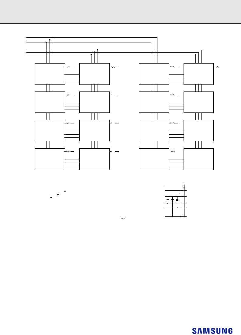
9. FUNCTION BLOCK DIAGRAM:
9.1 128GB, 16Gx72 Module
9.1.1 (PC4-RDIMM Populated as 2 physical ranks / 2 logical ranks of x4 DDR4 SDRAMs)
BG[1:0] |
|
|
QABG[1:0] -> BG[1:0]: SDRAMs D[20:1] |
|
|||||||
|
|
|
QBBG[1:0] -> BG[1:0]: SDRAMs D[36:21] |
|
|||||||
BA[1:0] |
|
|
QABA[1:0] -> BA[1:0]: SDRAMs D[20:1] |
|
|||||||
|
|
|
QBBA[1:0] -> BA[1:0]: SDRAMs D[36:21] |
|
|||||||
A[17:0] |
|
|
QAA[17:0] -> A[17:0]: SDRAMs D[20:1] |
|
|||||||
|
|
|
QBA[17:0] -> A[17:0]: SDRAMs D[36:21] |
|
|||||||
ACT_n |
|
|
QAACT_n -> ACT_n: SDRAMs D[20:1] |
|
|||||||
|
|
R |
QBACT_n -> ACT_n: SDRAMs D[36:21] |
|
|||||||
C[2:0] |
|
QAC[2:0] -> C[2:0]: SDRAMs D[20:1] |
|
||||||||
|
|
QBC[2:0] -> C[2:0]: SDRAMs D[36:21] |
|
||||||||
PARITY |
|
e |
QAPAR -> PAR: SDRAMs D[20:1] |
|
|
||||||
|
|
QBPAR -> PAR: SDRAMs D[36:21] |
|
|
|||||||
CKE0 |
|
g |
QACKE0 -> CKE: SDRAMs D[10:1] |
|
|
||||||
|
|
QBCKE0 -> CKE: SDRAMs D[28:21] |
|
||||||||
CKE1 |
|
i |
QACKE1 -> CKE: SDRAMs D[20:11] |
|
|||||||
|
|
QBCKE1 -> CKE: SDRAMs D[36:29] |
|
||||||||
ODT0 |
|
s |
QAODT0 -> ODT: SDRAMs D[10:1] |
|
|
||||||
|
|
QBODT0 -> ODT: SDRAMs D[28:21] |
|
||||||||
ODT1 |
|
t |
QAODT1 -> ODT: SDRAMs D[20:11] |
|
|||||||
|
|
QBODT1 -> ODT: SDRAMs D[36:29] |
|
||||||||
CS0_n |
|
e |
QACS0_n -> CS_n: SDRAMs D[10:1] |
|
|||||||
|
|
QBCS0_n -> CS_n: SDRAMs D[28:21] |
|
||||||||
CS1_n |
|
r. |
QACS1_n -> CS_n: SDRAMs D[20:11] |
|
|||||||
|
|
QBCS1_n -> CS_n: SDRAMs D[36:29] |
|
||||||||
CK0_t |
|
|
Y0_t -> CK_t: SDRAMs D[24:21], D[32:29] |
|
|||||||
|
|
|
Y1_t -> CK_t: SDRAMs D[5:1], D[15:11] |
|
|||||||
|
|
|
Y2_t -> CK_t: SDRAMs D[28:25], D[36:33] |
|
|||||||
CK0_c |
|
|
Y3_t -> CK_t: SDRAMs D[10:6], D[20:16] |
|
|||||||
|
|
Y0_c -> CK_c: SDRAMs D[24:21], D[32:29] |
|||||||||
|
|
|
|||||||||
CK1_t |
|
|
Y1_c -> CK_c: SDRAMs D[5:1], D[15:11] |
|
|||||||
|
|
Y2_c -> CK_c: SDRAMs D[28:25], D[36:33] |
|||||||||
|
|
|
|||||||||
CK1_c |
|
|
Y3_c -> CK_c: SDRAMs D[10:6], D[20:16] |
|
|||||||
RESET_n |
|
|
QRST_n -> RESET_n: All SDRAMs |
|
|
||||||
ALERT_n |
|
|
ERROR_IN_n <- ALERT_n: All SDRAMs |
|
|||||||
|
D1 |
D2 |
D3 |
D4 |
D5 |
Register |
D21 |
D22 |
D23 |
D24 |
|
Front |
D6 |
D7 |
D8 |
D9 |
D10 |
D25 |
D26 |
D27 |
D28 |
||
|
|||||||||||
|
|
||||||||||
Back |
D16 |
D17 |
D18 |
D19 |
D20 |
|
D33 |
D34 |
D35 |
D36 |
|
|
|
|
|
|
|
|
|
|
|
||
D11 |
D12 |
D13 |
D14 |
D15 |
D29 |
D30 |
D31 |
D32 |
Address, Command and Control lines
NOTE :
1)CK0_t, CK0_c terminated with 120 ± 5% resistor.
2)CK1_t, CK1_c terminated with 120 ± 5% resistor but not used.
3)Unless otherwise noted resistors are 22 ± 5%.
- 12 -

Registered DIMM
datasheet |
Rev. 1.0 |
DDR4 SDRAM |
QACS0_n
QAODT0
QACKE0
QACS1_n
QAODT1
QACKE1
|
|
|
|
|
CKE ODT CS n |
DQS0_t |
|
|
|
DQS_t |
D6 |
|
|
||||
DQS0_c |
|
|
|
DQS_c |
|
|
|
||||
DQ[3:0] |
|
|
|
DQ[3:0] |
|
|
|
||||
|
|
|
|
|
|
ZQ 


 VSS
VSS
DQS_t
DQS_c
DQ[3:0]
CKE ODT n _ ZQ CS
D16
VSS |
|
CKE ODT CSn |
|||
|
|
||||
DQS9_t |
|
|
|
DQS_t |
D1 |
|
|
||||
DQS9_c |
|
|
|
DQS_c |
|
|
|
||||
DQ[7:4] |
|
|
|
DQ[3:0] |
|
|
|
||||
|
|
|
|
|
|
ZQ 


 VSS
VSS
CKE
DQS_t
DQS_c
DQ[3:0]
ODT CSn |
|
|
|
|
ZQ |
|
|
|
VSS |
D11
|
|
|
|
|
CKE ODT CS n |
DQS1_t |
|
|
|
DQS_t |
D7 |
|
|
||||
DQS1_c |
|
|
|
DQS_c |
|
|
|
||||
DQ[11:8] |
|
|
|
DQ[3:0] |
|
|
|
||||
|
|
|
|
|
|
ZQ 


 VSS
VSS
CKE ODT n _ ZQ CS
DQS_t
DQS_c D17 DQ[3:0]
VSS |
|
CKE ODT CSn |
|||
|
|
||||
DQS10_t |
|
|
|
DQS_t |
D2 |
|
|
||||
DQS10_c |
|
|
|
DQS_c |
|
|
|
||||
DQ[15:12] |
|
|
|
DQ[3:0] |
|
|
|
||||
|
|
|
|
|
|
ZQ 


 VSS
VSS
CKE
DQS_t
DQS_c
DQ[3:0]
ODT CSn |
|
|
|
VSS |
ZQ |
|
|
|
D12
|
|
|
|
|
CKE ODT CS n |
DQS2_t |
|
|
|
DQS_t |
D8 |
|
|
||||
DQS2_c |
|
|
|
DQS_c |
|
|
|
||||
DQ[19:16] |
|
|
|
DQ[3:0] |
|
|
|
||||
|
|
|
|
|
|
ZQ 


 VSS
VSS
CKE ODT n _ ZQ CS
DQS_t
DQS_c D18 DQ[3:0]
VSS |
|
CKE ODT CSn |
|||
|
|
||||
DQS11_t |
|
|
|
DQS_t |
D3 |
|
|
||||
DQS11_c |
|
|
|
DQS_c |
|
|
|
||||
DQ[23:20] |
|
|
|
DQ[3:0] |
|
|
|
||||
|
|
|
|
|
|
ZQ 


 VSS
VSS
CKE
DQS_t
DQS_c
DQ[3:0]
ODT CSn |
|
|
|
VSS |
ZQ |
|
|
|
D13
|
|
|
|
|
CKE ODT CS n |
DQS3_t |
|
|
|
DQS_t |
D9 |
|
|
||||
DQS3_c |
|
|
|
DQS_c |
|
|
|
||||
DQ[27:24] |
|
|
|
DQ[3:0] |
|
|
|
||||
|
|
|
|
|
|
ZQ 


 VSS
VSS
CKE ODT n_ ZQ
CS
DQS_t
DQS_c D19 DQ[3:0]
VSS |
|
CKE ODT CSn |
|||
|
|
||||
DQS12_t |
|
|
|
DQS_t |
D4 |
|
|
||||
DQS12_c |
|
|
|
DQS_c |
|
|
|
||||
DQ[31:28] |
|
|
|
DQ[3:0] |
|
|
|
||||
|
|
|
|
|
|
ZQ 


 VSS
VSS
CKE
DQS_t
DQS_c
DQ[3:0]
ODT CSn |
|
|
|
VSS |
ZQ |
|
|
|
D14
CKE
DQS8_t 


 DQS_t DQS8_c


 DQS_c CB[3:0]


 DQ[3:0]
ODT
n |
ZQ |
|
CS |
||
|
D10
VSS
DQS_t
DQS_c
DQ[3:0]
CKE ODT
n |
ZQ |
|
CS |
||
|
D20
VSS |
|
CKE ODT CSn |
|||
|
|
||||
DQS17_t |
|
|
|
DQS_t |
D5 |
|
|
||||
DQS17_c |
|
|
|
DQS_c |
|
|
|
||||
CB[7:4] |
|
|
|
DQ[3:0] |
|
|
|
||||
|
|
|
|
|
|
ZQ 


 VSS
VSS
CKE
DQS_t
DQS_c
DQ[3:0]
ODT CSn |
|
|
|
VSS |
ZQ |
|
|
|
D15
NOTE :
1)Unless otherwise noted, resistor values are 15 ± 5%.
2)See the Net Structure diagrams for all resistors associated with the command, address and Control bus.
3)ZQ resistors are 240 ± 1%. For all other resistor values refer to the appropriate wiring diagram.
4)DRAM TEN pin need to be tied to VSS.
- 13 -
Registered DIMM
datasheet |
Rev. 1.0 |
DDR4 SDRAM |
QBCS0_n
QBODT0
QBCKE0
QBCS1_n
QBODT1
QBCKE1
ODT
CKE
DQS4_t 


 DQS_t DQS4_c


 DQS_c DQ[35:32]


 DQ[3:0]
n |
ZQ |
|
CS |
||
|
D25
VSS
DQS_t
DQS_c
DQ[3:0]
CKE
ODT
n |
ZQ |
|
CS |
||
|
D33
VSS
DQS13_t 


 DQS_t DQS13_c


 DQS_c DQ[39:36]


 DQ[3:0]
CKE ODT
n |
ZQ |
|
CS |
||
|
D21
VSS
DQS_t
DQS_c
DQ[3:0]
CKE
ODT
n |
|
|
|
|
|
CS |
ZQ |
|
|
|
VSS |
|
|
||||
|
|
|
|
|
D29
ODT
CKE
DQS5_t 


 DQS_t DQS5_c


 DQS_c DQ[43:40]


 DQ[3:0]
n_ ZQ 
 CS
CS
D26
VSS
DQS_t
DQS_c
DQ[3:0]
CKE
ODT
n_ ZQ 
 CS
CS
D34
VSS
DQS14_t 


 DQS_t DQS14_c


 DQS_c DQ[47:44]


 DQ[3:0]
CKE ODT
n_ ZQ 
 CS
CS
D22
VSS
DQS_t
DQS_c
DQ[3:0]
CKE
ODT
CSn |
|
|
|
VSS |
ZQ |
|
|
|
D30
ODT
CKE
DQS6_t 


 DQS_t DQS6_c


 DQS_c DQ[51:48]


 DQ[3:0]
n |
ZQ |
|
CS |
||
|
D27
VSS
DQS_t
DQS_c
DQ[3:0]
CKE
ODT
n |
ZQ |
|
CS |
||
|
D35
VSS
DQS15_t 


 DQS_t DQS15_c


 DQS_c DQ[55:52]


 DQ[3:0]
CKE ODT
n |
ZQ |
|
CS |
||
|
D23
VSS
DQS_t
DQS_c
DQ[3:0]
CKE
ODT
n |
|
|
|
|
|
CS |
ZQ |
|
|
|
VSS |
|
|
||||
|
|
|
|
|
D31
ODT
CKE
DQS7_t 


 DQS_t DQS7_c


 DQS_c DQ[59:56]


 DQ[3:0]
n |
|
CS_ |
ZQ |
|
D28
VSS
DQS_t
DQS_c
DQ[3:0]
CKE
ODT
n |
|
CS_ |
ZQ |
|
D36
VSS
DQS16_t 


 DQS_t DQS16_c


 DQS_c DQ[63:60]


 DQ[3:0]
CKE
ODT CSn |
|
|
|
VSS |
ZQ |
|
|
|
D24
VDDSPD
SA2 |
|
|
|
|
|
|
|
|
|
|
|
|
|
|
|
VPP |
|
|
|
|
|
|
|
|
|
|
|
|
|
|
|
||
SA1 |
|
|
|
|
|
|
|
|
|
|
|
|
|
|
|
VDD |
|
|
|
|
|
|
|
|
|
|
|
|
|
|
|
||
SA0 |
|
|
|
|
|
|
|
|
|
|
|
|
|
|
|
|
|
|
|
|
|
|
|
|
|
|
|
|
|
|
|
||
|
|
SA0 SA1 SA2 |
|
SA0 SA1 SA2 |
|
|
|
|
|
VTT |
||||||
SCL |
|
SCL |
|
SCL |
|
BFUNC |
|
|
|
|
VSS |
VREFCA |
||||
|
|
|
|
|
|
|
|
|||||||||
SDA |
|
SDA |
|
SDA |
|
|
|
|
|
VSS |
||||||
|
|
|
|
|||||||||||||
|
|
|
|
|
|
|||||||||||
|
|
|
|
EVENT_n |
|
|
|
ZQCAL |
|
|
|
|
VSS |
|||
|
|
|
|
|
|
|
|
|
|
|
||||||
|
|
Serial PD with |
|
|
Register |
|
|
|
|
|
|
|||||
|
|
Thermal sensor |
|
|
|
|
|
|
|
|
|
|
|
|||
NOTE :
1)Unless otherwise noted, resistor values are 15 ± 5%.
2)See the Net Structure diagrams for all resistors associated with the command, address and control bus.
3)ZQ resistors are 240 ±1%. For all other resistor values refer to the appropriate wiring diagram.
4)DRAM TEN pin need to be tied to VSS.
ODT
CKE
DQS_t
DQS_c
DQ[3:0]
Serial PD
D1-D36
D1-D36
D1-D36
D1-D36
D1-D36
n |
|
|
|
|
|
CS_ |
ZQ |
|
|
|
VSS |
|
|
|
|
D32
- 14 -

Registered DIMM
datasheet |
Rev. 1.0 |
DDR4 SDRAM |
10. ABSOLUTE MAXIMUM RATINGS
[Table 5] Absolute Maximum DC Ratings
Symbol |
Parameter |
Rating |
Units |
NOTE |
|
|
|
|
|
VDD |
Voltage on VDD pin relative to Vss |
-0.3 ~ 1.5 |
V |
1,3 |
|
|
|
|
|
VDDQ |
Voltage on VDDQ pin relative to Vss |
-0.3 ~ 1.5 |
V |
1,3 |
|
|
|
|
|
VPP |
Voltage on VPP pin relative to Vss |
-0.3 ~ 3.0 |
V |
4 |
|
|
|
|
|
VIN, VOUT |
Voltage on any pin except VREFCA relative to Vss |
-0.3 ~ 1.5 |
V |
1,3,5 |
TSTG |
Storage Temperature |
-55 to +100 |
°C |
1,2 |
NOTE :
1)Stresses greater than those listed under “Absolute Maximum Ratings” may cause permanent damage to the device. This is a stress rating only and functional operation of the device at these or any other conditions above those indicated in the operational sections of this specification is not implied. Exposure to absolute maximum rating conditions for extended periods may affect reliability
2)Storage Temperature is the case surface temperature on the center/top side of the DRAM. For the measurement conditions, please refer to JESD51-2 standard.
3)VDD and VDDQ must be within 300mV of each other at all times; and VREFCA must be not greater than 0.6 x VDDQ, When VDD and VDDQ are less than 500mV; VREFCA may be equal to or less than 300mV
4)VPP must be equal or greater than VDD/VDDQ at all times.
5)Overshoot area above 1.5 V is specified in 12.3.4, 12.3.5Clock Overshoot and Undershoot Specifications and 12.3.6.
11. AC & DC OPERATING CONDITIONS
[Table 6] Recommended DC Operating Conditions
Symbol |
Parameter |
|
Rating |
|
Unit |
NOTE |
|
Min. |
Typ. |
Max. |
|||||
|
|
|
|
||||
VDD |
Supply Voltage |
1.14 |
1.2 |
1.26 |
V |
1,2,3 |
|
|
|
|
|
|
|
|
|
VDDQ |
Supply Voltage for Output |
1.14 |
1.2 |
1.26 |
V |
1,2,3 |
|
|
|
|
|
|
|
|
|
VPP |
Peak-to-Peak Voltage |
2.375 |
2.5 |
2.75 |
V |
3 |
|
|
|
|
|
|
|
|
NOTE :
1)Under all conditions VDDQ must be less than or equal to VDD.
2)VDDQ tracks with VDD. AC parameters are measured with VDD and VDDQ tied together.
3)DC bandwidth is limited to 20MHz.
- 15 -

Registered DIMM
datasheet |
Rev. 1.0 |
DDR4 SDRAM |
12. AC & DC INPUT MEASUREMENT LEVELS
12.1 AC & DC Logic Input Levels for Single-Ended Signals
[Table 7] Single-ended AC & DC Input Levels for Command and Address
Symbol |
Parameter |
DDR4-1600/1866/2133/2400 |
DDR4-2666/2933 |
Unit |
NOTE |
|||
Min. |
Max. |
Min. |
Max. |
|||||
|
|
|
|
|||||
VIH.CA(DC75) |
DC input logic high |
VREFCA+ 0.075 |
VDD |
- |
- |
V |
|
|
VIH.CA(DC65) |
- |
- |
VREFCA+ 0.065 |
VDD |
|
|||
|
|
|
||||||
VIL.CA(DC75) |
DC input logic low |
VSS |
VREFCA-0.075 |
- |
- |
V |
|
|
VIL.CA(DC65) |
- |
- |
VSS |
VREFCA-0.065 |
|
|||
|
|
|
||||||
VIH.CA(AC100) |
AC input logic high |
VREF + 0.1 |
Note 2 |
- |
- |
V |
|
|
VIH.CA(AC90) |
- |
- |
VREF + 0.09 |
Note 2 |
1 |
|||
|
|
|||||||
VIL.CA(AC100) |
AC input logic low |
Note 2 |
VREF - 0.1 |
- |
- |
V |
|
|
VIL.CA(AC90) |
- |
- |
Note 2 |
VREF - 0.09 |
1 |
|||
|
|
|||||||
VREFCA(DC) |
Reference Voltage for ADD, CMD inputs |
0.49*VDD |
0.51*VDD |
0.49*VDD |
0.51*VDD |
V |
2,3 |
|
|
|
|
|
|
|
|
|
|
NOTE :
1)See “Overshoot and Undershoot Specifications” on section12.3AC and DC Logic Input Levels for Differential Signals.
2)The AC peak noise on VREFCA may not allow VREFCA to deviate from VREFCA(DC) by more than ± 1% VDD (for reference : approx. ± 12mV)
3)For reference : approx. VDD/2 ± 12mV.
12.2 AC and DC Input Measurement Levels: VREF Tolerances.
The DC-tolerance limits and ac-noise limits for the reference voltages VREFCA is illustrated in Figure 1. It shows a valid reference voltage VREF(t) as a function of time. (VREF stands for VREFCA).
VREF(DC) is the linear average of VREF(t) over a very long period of time (e.g. 1 sec). This average has to meet the min/max requirement in Table 7. Furthermore VREF(t) may temporarily deviate from VREF(DC) by no more than ± 1% VDD.
voltage |
VDD |
VSS |
time |
Figure 1. Illustration of VREF(DC) tolerance and VREF AC-noise limits
The voltage levels for setup and hold time measurements VIH(AC), VIH(DC), VIL(AC) and VIL(DC) are dependent on VREF.
"VREF" shall be understood as VREF(DC), as defined in Figure 1.
This clarifies, that DC-variations of VREF affect the absolute voltage a signal has to reach to achieve a valid high or low level and therefore the time to which setup and hold is measured. System timing and voltage budgets need to account for VREF(DC) deviations from the optimum position within the
data-eye of the input signals.
This also clarifies that the DRAM setup/hold specification and derating values need to include time and voltage associated with VREF AC-noise. Timing and voltage effects due to AC-noise on VREF up to the specified limit (+/-1% of VDD) are included in DRAM timings and their associated deratings.
- 16 -

Registered DIMM
datasheet |
Rev. 1.0 |
DDR4 SDRAM |
12.3 AC and DC Logic Input Levels for Differential Signals
12.3.1 Differential Signals Definition
|
|
|
|
|
|
|
|
|
|
|
|
|
|
|
|
|
|
tDVAC |
|||||||||||||||||||||||
|
|
|
|
VIH.DIFF.AC.MIN |
|
|
|
|
|
|
|
|
|
|
|
|
|||||||||||||||||||||||||
|
|
|
|
|
|
|
|
|
|
|
|
|
|
|
|
|
|
|
|
|
|
|
|
|
|
|
|
|
|
|
|
|
|
|
|
|
|
|
|
||
|
|
|
|
|
|
|
|
|
|
|
|
|
|
|
|
|
|
|
|
|
|
|
|
|
|
|
|
|
|
|
|
|
|
|
|
|
|
|
|
||
|
|
c) |
|
VIH.DIFF.MIN |
|
|
|
|
|
|
|
|
|
|
|
|
|
|
|
|
|
|
|
|
|
|
|
|
|
|
|
|
|
|
|
|
|
|
|||
|
|
|
|
|
|
|
|
|
|
|
|
|
|
|
|
|
|
|
|
|
|
||||||||||||||||||||
|
|
|
|
|
|
|
|
|
|
|
|
|
|
|
|
|
|
|
|
|
|
|
|
|
|
|
|
|
|
|
|
|
|
|
|
|
|
|
|
|
|
|
|
-CK)t - CK |
0.0 |
|
|
|
|
|
|
|
|
|
|
|
|
|
|
|
|
|
|
|
|
|
|
|
|
|
|
|
|
|
|
|
|
|
|
|
|
|
|
|
|
|
|
|
|
|
|
|
|
|
|
|
|
|
|
|
|
|
|
|
|
|
|
|
|
|
|
|
|
|
|
|
|
|
|
|
|
||||
|
|
|
|
|
|
|
|
|
|
|
|
|
|
|
|
|
|
|
|
|
|
|
|
|
|
|
|
|
|
|
|
|
|
|
|
|
|||||
|
(CK |
|
|
|
|
|
|
|
|
|
|
half cycle |
|||||||||||||||||||||||||||||
Voltage |
VIL.DIFF.MAX |
|
|
|
|
|
|
|
|
|
|
|
|
|
|
|
|
|
|
|
|
|
|
|
|
|
|
|
|
|
|
|
|
|
|
|
|
||||
|
|
|
|
|
|
|
|
|
|
|
|
|
|
|
|
|
|
|
|
||||||||||||||||||||||
Input |
|
|
|
|
|
|
|
|
|
|
|
|
|
|
|
|
|
|
|
|
|
|
|
|
|
|
|
|
|
|
|
|
|
|
|
|
|
|
|||
Differential |
VIL.DIFF.AC.MAX |
|
|
|
|
|
|
|
|
|
|
|
|
|
|
|
|
|
|
|
|
|
|
|
|
|
|
|
|
|
|
|
|
|
|
|
|
||||
|
|
|
|
|
|
|
|
|
|
|
|
|
|
|
|
|
|
|
|
|
|
|
|
|
|
|
|
|
|
|
|
|
|
|
tDVAC |
||||||
|
|
|
|
|
|
|
|
|
|
|
|
|
|
|
|
|
|
|
|
|
|
|
|
|
|
|
|
|
|
|
|
|
|
|
|
|
|||||
|
|
|
|
|
|
|
|
|
|
|
|
|
|
|
|
|
|
|
|
|
|
|
|
|
|
|
|
|
|
|
|
|
|
|
|
|
|||||
|
|
|
|
|
|
|
|
|
|
|
|
|
|
|
|
|
|
|
|
|
|
|
|
|
|
|
|
|
|
|
|
|
|
|
|
|
|
|
|
|
|
time
Figure 2. Definition of differential ac-swing and “time above ac-level” tDVAC
NOTE:
1)Differential signal rising edge from VIL.DIFF.MAX to VIH.DIFF.MIN must be monotonic slope.
2)Differential signal falling edge from VIH.DIFF.MIN to VIL.DIFF.MAX must be monotonic slope.
12.3.2 Differential Swing Requirements for Clock (CK_t - CK_c)
[Table 8] Differential AC and DC Input Levels
Symbol |
Parameter |
DDR4 -1600/1866/2133 |
DDR4 -2400/2666 |
DDR4-2933 |
unit |
NOT |
||||
min |
max |
min |
max |
min |
max |
E |
||||
|
|
|
||||||||
VIHdiff |
differential input high |
+0.150 |
NOTE 3 |
+0.135 |
NOTE 3 |
+0.125 |
NOTE 3 |
V |
1 |
|
VILdiff |
differential input low |
NOTE 3 |
-0.150 |
NOTE 3 |
-0.135 |
NOTE 3 |
-0.125 |
V |
1 |
|
VIHdiff(AC) |
differential input high ac |
2 x (VIH(AC) - |
NOTE 3 |
2 x (VIH(AC) - |
NOTE 3 |
2 x (VIH(AC) - |
NOTE 3 |
V |
2 |
|
VREF) |
VREF) |
VREF) |
||||||||
|
|
|
|
|
|
|
||||
VILdiff(AC) |
differential input low ac |
NOTE 3 |
2 x (VIL(AC) - |
NOTE 3 |
2 x (VIL(AC) - |
NOTE 3 |
2 x (VIL(AC) - |
V |
2 |
|
VREF) |
VREF) |
VREF) |
||||||||
|
|
|
|
|
|
|
||||
NOTE :
1)Used to define a differential signal slew-rate.
2)for CK_t - CK_c use VIH.CA/VIL.CA(AC) of ADD/CMD and VREFCA;
3)These values are not defined; however, the differential signals CK_t - CK_c, need to be within the respective limits (VIH.CA(DC) max, VIL.CA(DC)min) for single-ended signals as well as the limitations for overshoot and undershoot.
[Table 9] Allowed Time Before Ringback (tDVAC) for CK_t - CK_c
Slew Rate [V/ns] |
|
tDVAC [ps] @ |VIH/Ldiff(AC)| = 200mV |
|
|
min |
|
max |
> 4.0 |
120 |
|
- |
|
|
|
|
4.0 |
115 |
|
- |
|
|
|
|
3.0 |
110 |
|
- |
|
|
|
|
2.0 |
105 |
|
- |
|
|
|
|
1.8 |
100 |
|
- |
|
|
|
|
1.6 |
95 |
|
- |
|
|
|
|
1.4 |
90 |
|
- |
|
|
|
|
1.2 |
85 |
|
- |
|
|
|
|
1.0 |
80 |
|
- |
|
|
|
|
< 1.0 |
80 |
|
- |
|
|
|
|
- 17 -

Registered DIMM
datasheet |
Rev. 1.0 |
DDR4 SDRAM |
12.3.3 Single-ended Requirements for Differential Signals
Each individual component of a differential signal (CK_t, CK_c) has also to comply with certain requirements for single-ended signals.
CK_t and CK_c have to approximately reach VSEHmin / VSELmax (approximately equal to the ac-levels (VIH.CA(AC) / VIL.CA(AC)) for ADD/CMD signals) in every half-cycle.
Note that the applicable ac-levels for ADD/CMD might be different per speed-bin etc. E.g., if Different value than VIH.CA(AC100)/VIL.CA(AC100) is used for ADD/CMD signals, then these ac-levels apply also for the single-ended signals CK_t and CK_c.
VDD or VDDQ
VSEH min
VDD/2 or VDDQ/2 |
|
|
|
|
|
|
|
|
|
|
|
|
|
|
|
|
|
|
|
|
|
|
|
|
|
|
|
|
|
|
|
|
|
|
|
|
CK |
||
|
|
|
|
|
|
|
|
|
|
|
|
|
|
|
|
|
|
|
|
|
|
|
|
|
|
|
|
|
|
|
|
|
|
|
|
||||
|
|
|
|
|
|
|
|
|
|
|
|
|
|
|
|
|
|
|
|
|
|
|
|
|
|
|
|
|
|
|
|
|
|
|
|
|
|
||
|
VSEL max |
|
|
|
|
|
|
|
|
|
|
|
|
|
|
|
|
|
|
|
|
|
|
|
|
|
|
|
|
|
|
|
|
|
|
|
|
|
|
|
|
|
|
|
|
|
|
|
|
|
|
|
|
|
|
|
|
|
|
|
|
|
|
|
|
|
|
|
|
VSEL |
|||||||||
|
VSS or VSSQ |
|
|
|
|
|
|
|
|
|
|
|
|
|
|
|
|
|
|
|
|
|
|
|
|
|
|
|
|
|
|
||||||||
|
|
|
|
|
|
|
|
|
|
|
|
|
|
|
|
|
|
|
|
|
|
|
|
|
|
|
|
|
|
|
|||||||||
|
|
|
|
|
|
|
|
|
|
|
|
|
|
|
|
|
|
|
|
|
|
|
|
|
|
|
|
|
|
|
|
|
|
|
|
|
|
time |
|
|
|
|
|
|
|
|
|
|
|
|
|
|
|
|
|
|
|
|
|
|
|
|
|
|
|
|
|
|
|
|
|
|
|
|
|
||||
|
|
|
|
|
|
|
|
|
|
|
|
|
|
|
|
|
|
|
|
|
|
|
|
|
|
|
|
|
|
|
|
|
|
|
|
|
|
|
|
Figure 3. Single-ended requirement for differential signals.
Note that, while ADD/CMD signal requirements are with respect to VrefCA, the single-ended components of differential signals have a requirement with respect to VDD / 2; this is nominally the same. The transition of single-ended signals through the ac-levels is used to measure setup time. For singleended components of differential signals the requirement to reach VSELmax, VSEHmin has no bearing on timing, but adds a restriction on the common mode characteristics of these signals.
[Table 10] Single-ended Levels for CK_t, CK_c
Symbol |
Parameter |
DDR4-1600/1866/2133 |
DDR4-2400/2666 |
DDR4-2933 |
Unit |
NOTE |
||||
Min |
Max |
Min |
Max |
Min |
Max |
|||||
|
|
|
|
|||||||
VSEH |
Single-ended high-level for |
(VDD/2)+0.100 |
NOTE3 |
(VDD/2)+0.95 |
NOTE3 |
(VDD/2)+0.85 |
NOTE3 |
V |
1, 2 |
|
CK_t, CK_c |
||||||||||
|
|
|
|
|
|
|
|
|
||
|
|
|
|
|
|
|
|
|
|
|
VSEL |
Single-ended low-level for CK_t, |
NOTE3 |
(VDD/2)-0.100 |
NOTE3 |
(VDD/2)-0.95 |
NOTE3 |
(VDD/2)-0.85 |
V |
1, 2 |
|
CK_c |
||||||||||
|
|
|
|
|
|
|
|
|
||
|
|
|
|
|
|
|
|
|
|
|
NOTE : |
|
|
|
|
|
|
|
|
|
|
1)For CK_t - CK_c use VIH.CA/VIL.CA(AC) of ADD/CMD;
2)VIH(AC)/VIL(AC) for ADD/CMD is based on VREFCA;
3)These values are not defined, however the single-ended signals CK_t - CK_c need to be within the respective limits (VIH.CA(DC) max, VIL.CA(DC)min) for single-ended signals as well as the limitations for overshoot and undershoot.
- 18 -

Registered DIMM
datasheet |
Rev. 1.0 |
DDR4 SDRAM |
12.3.4 Address, Command and Control Overshoot and Undershoot specifications
[Table 11] AC overshoot/undershoot specification for Address, Command and Control pins
|
|
|
|
Specification |
|
|
|
|
||
Parameter |
Symbol |
DDR4- |
DDR4- |
DDR4- |
|
DDR4- |
DDR4- |
DDR4- |
Unit |
NOTE |
|
|
1600 |
1866 |
2133 |
|
2400 |
2666 |
2933 |
|
|
Maximum peak amplitude above VAOS |
VAOSP |
|
|
|
0.06 |
|
|
V |
|
|
|
|
|
|
|
|
|
|
|
||
Upper boundary of overshoot area AAOS1 |
VAOS |
|
|
VDD +0.24 |
|
|
V |
1 |
||
|
|
|
|
|
|
|
|
|
|
|
Maximum peak amplitude allowed for undershoot |
VAUS |
|
|
|
0.30 |
|
|
V |
|
|
|
|
|
|
|
|
|
|
|
|
|
Maximum overshoot area per 1 tCK above VAOS |
AAOS2 |
0.0083 |
0.0071 |
0.0062 |
|
0.0055 |
0.0055 |
0.0055 |
V-ns |
|
|
|
|
|
|
|
|
|
|
|
|
Maximum overshoot area per 1 tCK between VDD and |
AAOS1 |
0.2550 |
0.2185 |
0.1914 |
|
0.1699 |
0.1699 |
0.1699 |
V-ns |
|
VAOS |
|
|
|
|
|
|
|
|
|
|
Maximum undershoot area per 1 tCK below VSS |
AAUS |
0.2644 |
0.2265 |
0.1984 |
|
0.1762 |
0.1762 |
0.1762 |
V-ns |
|
|
|
|
|
|
|
|
|
|
|
|
(A0-A13,A17,BG0-BG1,BA0-BA1,ACT_n,RAS_n/A16,CAS_n/A15,WE_n/A14,CS_n,CKE,ODT,C2-C0) |
|
|
|
|||||||
|
|
|
|
|
|
|
|
|
|
|
NOTE :
1)The value of VAOS matches VDD absolute max as defined in Table 5 Absolute Maximum DC Ratings if VDD equals VDD max as defined in Table 6 Recommended DC Operating Conditions. If VDD is above the recommended operating conditions, VAOS remains at VDD absolute max as defined in Table 5.
|
VAOSP |
|
|
|
|
|
|
|
|
|
AAOS2 |
|||||||
|
|
|
|
|
|
|
|
|
|
|||||||||
|
VAOS |
|
|
|
|
|
|
|
|
|
||||||||
|
|
|
|
|
|
|
|
|
|
|
|
|
AAOS1 |
|||||
|
|
|
|
|
|
|
|
|
|
|
|
|
||||||
Volts |
VDD |
|
|
|
|
|
|
|
|
|
|
|
|
|
|
|
||
|
|
|
|
|
|
|
1 tCK |
|
||||||||||
(V) |
VSS |
|
|
|
|
|
|
|
|
|
|
|
|
|
|
|
|
|
|
|
|
|
|
|
|
|
|
|
|
|
|
|
|
|
|||
|
|
|
|
|
|
|
|
|
|
|
|
|
|
AAUS |
||||
|
V |
|
|
|
|
|
|
|
|
|
|
|
||||||
|
|
|
|
|
|
|
|
|
||||||||||
|
AUS |
|
|
|
|
|
|
|
|
|
|
|
|
|
||||
|
|
|
|
|
|
|
|
|
|
|
|
|
|
|
|
|
|
|
Figure 4. Address, Command and Control Overshoot and Undershoot Definition
- 19 -
Registered DIMM
datasheet |
Rev. 1.0 |
DDR4 SDRAM |
12.3.5 Clock Overshoot and Undershoot Specifications
[Table 12] AC overshoot/undershoot specification for Clock
|
|
|
|
Specification |
|
|
|
|
||
Parameter |
Symbol |
DDR4- |
DDR4- |
DDR4- |
|
DDR4- |
DDR4- |
DDR4- |
Unit |
NOTE |
|
|
1600 |
1866 |
2133 |
|
2400 |
2666 |
2933 |
|
|
Maximum peak amplitude above VCOS |
VCOSP |
|
|
|
0.06 |
|
|
V |
|
|
|
|
|
|
|
|
|
|
|
||
Upper boundary of overshoot area ADOS1 |
VCOS |
|
|
VDD +0.24 |
|
|
V |
1 |
||
|
|
|
|
|
|
|
|
|
|
|
Maximum peak amplitude allowed for undershoot |
VCUS |
|
|
|
0.30 |
|
|
V |
|
|
|
|
|
|
|
|
|
|
|
|
|
Maximum overshoot area per 1 UI above VCOS |
ACOS2 |
0.0038 |
0.0032 |
0.0028 |
|
0.0025 |
0.0025 |
0.0025 |
V-ns |
|
|
|
|
|
|
|
|
|
|
|
|
Maximum overshoot area per 1 UI between VDD and |
ACOS1 |
0.1125 |
0.0964 |
0.0844 |
|
0.0750 |
0.0750 |
0.0750 |
V-ns |
|
VDOS |
|
|
|
|
|
|
|
|
|
|
Maximum undershoot area per 1 UI below VSS |
ACUS |
0.1144 |
0.0980 |
0.0858 |
|
0.0762 |
0.0762 |
0.0762 |
V-ns |
|
|
|
|
|
|
|
|
|
|
|
|
|
(CK_t, CK_c) |
|
|
|
|
|
|
|
|
|
|
|
|
|
|
|
|
|
|
|
|
NOTE : |
|
|
|
|
|
|
|
|
|
|
1)The value of VCOS matches VDD absolute max as defined in Table 5 Absolute Maximum DC Ratings if VDD equals VDD max as defined in Table 6 Recommended DC Operating Conditions. If VDD is above the recommended operating conditions, VCOS remains at VDD absolute max as defined in Table 5.
|
VCOSP |
|
|
|
|
|
|
|
|
|
ACOS2 |
|||||||
|
|
|
|
|
|
|
|
|
|
|||||||||
|
VCOS |
|
|
|
|
|
|
|
|
|
||||||||
|
|
|
|
|
|
|
|
|
|
|
|
|
ACOS1 |
|||||
|
|
|
|
|
|
|
|
|
|
|
|
|
||||||
Volts |
VDD |
|
|
|
|
|
|
|
|
|
|
|
|
|
|
|
||
|
|
|
|
|
|
|
1 UI |
|
||||||||||
(V) |
VSS |
|
|
|
|
|
|
|
|
|
|
|
|
|
|
|
|
|
|
|
|
|
|
|
|
|
|
|
|
|
|
|
|
|
|||
|
|
|
|
|
|
|
|
|
|
|
|
|
|
ACUS |
||||
|
VCUS |
|
|
|
|
|
|
|
|
|
|
|
||||||
|
|
|
|
|
|
|
|
|
||||||||||
|
|
|
|
|
|
|
|
|
|
|
|
|
|
|
|
|
|
|
Figure 5. Clock Overshoot and Undershoot Definition
- 20 -
Registered DIMM
datasheet |
Rev. 1.0 |
DDR4 SDRAM |
12.3.6 Data, Strobe and Mask Overshoot and Undershoot Specifications
[Table 13] AC overshoot/undershoot specification for Data, Strobe and Mask
|
|
|
|
Specification |
|
|
|
NOT |
||
Parameter |
Symbol |
DDR4- |
DDR4- |
DDR4- |
|
DDR4- |
DDR4- |
DDR4- |
Unit |
|
|
E |
|||||||||
|
|
1600 |
1866 |
2133 |
|
2400 |
2666 |
2933 |
|
|
|
|
|
|
|
||||||
Maximum peak amplitude above VDOS |
VDOSP |
|
|
|
0.16 |
|
|
V |
|
|
|
|
|
|
|
|
|
|
|
||
Upper boundary of overshoot area ADOS1 |
VDOS |
|
|
VDDQ + 0.24 |
|
|
V |
1 |
||
|
|
|
|
|
|
|
|
|
|
|
Lower boundary of undershoot area ADUS1 |
VDUS |
|
|
|
0.30 |
|
|
V |
2 |
|
|
|
|
|
|
|
|
|
|
|
|
Maximum peak amplitude below VDUS |
VDUSP |
0.10 |
0.10 |
0.10 |
|
0.10 |
0.10 |
0.10 |
V |
|
|
|
|
|
|
|
|
|
|
|
|
Maximum overshoot area per 1 UI above VDOS |
ADOS2 |
0.0150 |
0.0129 |
0.0113 |
|
0.0100 |
0.0100 |
0.0100 |
V-ns |
|
|
|
|
|
|
|
|
|
|
|
|
Maximum overshoot area per 1 UI between |
ADOS1 |
0.1050 |
0.0900 |
0.0788 |
|
0.0700 |
0.0700 |
0.0700 |
V-ns |
|
VDDQ and VDOS |
|
|
||||||||
|
|
|
|
|
|
|
|
|
|
|
|
|
|
|
|
|
|
|
|
|
|
Maximum undershoot area per 1 UI between |
ADUS1 |
0.1050 |
0.0900 |
0.0788 |
|
0.0700 |
0.0700 |
0.0700 |
V-ns |
|
VSSQ and VDUS1 |
|
|
||||||||
|
|
|
|
|
|
|
|
|
|
|
|
|
|
|
|
|
|
|
|
|
|
Maximum undershoot area per 1 UI below VDUS |
ADUS2 |
0.0150 |
0.0129 |
0.0113 |
|
0.0100 |
0.0100 |
0.0100 |
V-ns |
|
|
|
|
|
|
|
|
|
|
|
|
NOTE :
1)The value of VDOS matches (VIN, VOUT) max as defined in Table 5 Absolute Maximum DC Ratings if VDDQ equals VDDQ max as defined in Table 6 Recommended DC Operating Conditions. If VDDQ is above the recommended operating conditions, VDOS remains at (VIN, VOUT) max as defined in Table 5.
2)The value of VDUS matches (VIN, VOUT) min as defined in Table 5 Absolute Maximum DC Ratings
|
VDOSP |
|
|
|
|
|
|
|
|
ADOS2 |
||||||
|
|
|
|
|
|
|
|
|
||||||||
|
VDOS |
|
|
|
|
|
|
|
|
|||||||
|
|
|
|
|
|
|
|
|
|
|
ADOS1 |
|||||
Volts |
VDDQ |
|
|
|
|
|
|
|
|
|
|
|
|
|
||
|
|
|
|
|
|
|
1 UI |
|
||||||||
(V) |
VSSQ |
|
|
|
|
|
|
|
|
|
|
|
|
|
|
|
|
|
|
|
|
|
|
|
|
|
|
|
|
|
|||
|
|
|
|
|
|
|
|
|
|
|
|
|
|
|||
ADUS1
VDUSP
Figure 6. Data, Strobe and Mask Overshoot and Undershoot Definition
- 21 -

Registered DIMM
datasheet |
Rev. 1.0 |
DDR4 SDRAM |
12.4 Slew Rate Definitions
12.4.1 Slew Rate Definitions for Differential Input Signals (CK)
Input slew rate for differential signals (CK_t, CK_c) are defined and measured as shown in Table 14 and Figure 7.
[Table 14] Differential Input Slew Rate Definition
Description |
Measured |
Defined by |
||
from |
to |
|||
|
|
|||
Differential input slew rate for rising edge (CK_t - CK_c) |
VILdiffmax |
VIHdiffmin |
[VIHdiffmin - VILdiffmax] / DeltaTRdiff |
|
Differential input slew rate for falling edge (CK_t - CK_c) |
VIHdiffmin |
VILdiffmax |
[VIHdiffmin - VILdiffmax] / DeltaTFdiff |
|
NOTE :
1) The differential signal (i,e.,CK_t - CK_c) must be linear between these thresholds.
Delta TRdiff
Differential Input Voltage(i,e, CK_t - CK_c)
VIHdiffmin
0
VILdiffmax
Delta TFdiff
Figure 7. Differential Input Slew Rate Definition for CK_t, CK_c
- 22 -

Registered DIMM
datasheet |
Rev. 1.0 |
DDR4 SDRAM |
12.4.2 Slew Rate Definition for Single-ended Input Signals (CMD/ADD)
Delta TRsingle
VIHCA(AC) Min
VIHCA(DC) Min
VREFCA(DC)
VILCA(DC) Max
VILCA(AC) Max
Delta TFsingle
Figure 8. Single-ended Input Slew Rate definition for CMD and ADD
NOTE :
1)Single-ended input slew rate for rising edge = {VIHCA(AC)Min - VILCA(DC)Max} / Delta TR single.
2)Single-ended input slew rate for falling edge = {VIHCA(DC)Min - VILCA(AC)Max} / Delta TF single.
3)Single-ended signal rising edge from VILCA(DC)Max to VIHCA(DC)Min must be monotonic slope.
4)Single-ended signal falling edge from VIHCA(DC)Min to VILCA(DC)Max must be monotonic slope.
- 23 -
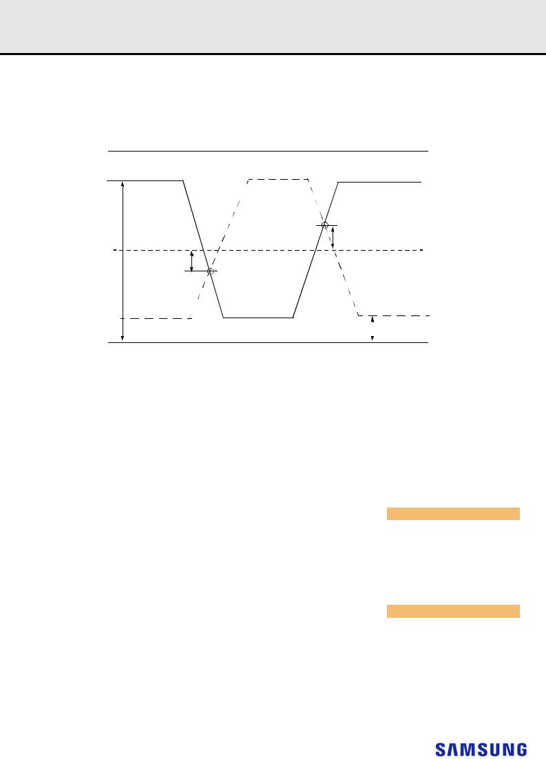
Registered DIMM
datasheet |
Rev. 1.0 |
DDR4 SDRAM |
12.5 Differential Input Cross Point Voltage
To guarantee tight setup and hold times as well as output skew parameters with respect to clock, each cross point voltage of differential input signals (CK_t, CK_c) must meet the requirements in Table 15. The differential input cross point voltage VIX is measured from the actual cross point of true and complement signals to the midlevel between of VDD and VSS.
VDD
CK_t
Vix
VDD/2
CK_c
VSEH |
VSEL |
VSS
Figure 9. Vix Definition (CK)
[Table 15] Cross Point Voltage for Differential Input Signals (CK)
Symbol |
Parameter |
|
|
DDR4-1600/1866/2133 |
|
|
|
min |
max |
||||
|
|
|
||||
|
|
VSEL < VDD/2 - |
|
VDD/2 - 145mV =< |
VDD/2 + 100mV =< |
VDD/2 + 145mV < |
- |
Area of VSEH, VSEL |
|
VSEL =< VDD/2 - |
VSEH =< VDD/2 + |
||
|
|
145mV |
|
100mV |
145mV |
VSEH |
|
|
|
|
|
||
|
|
|
|
|
|
|
VlX(CK) |
Differential Input Cross Point Voltage relative to |
-120mV |
|
-(VDD/2 - VSEL) + |
(VSEH - VDD/2) - |
120mV |
VDD/2 for CK_t, CK_c |
|
25mV |
25mV |
|||
|
|
|
|
|||
|
|
|
|
|
|
|
Symbol |
Parameter |
|
|
DDR4-2400 |
|
|
|
min |
max |
||||
|
|
|
||||
|
|
VSEL < |
|
VDD/2 - 145 mV |
VDD/2 + 100 mV |
VDD/2 + 145 mV < |
- |
Area of VSEH, VSEL |
|
=< VSEL =< |
=< VSEH =< |
||
VDD/2 - 145 mV |
|
VSEH |
||||
|
|
|
VDD/2 - 100 mV |
VDD/2 + 145 mV |
||
|
|
|
|
|
||
|
|
|
|
|
|
|
VlX(CK) |
Differential Input Cross Point Voltage relative to |
-120mV |
|
- (VDD/2 - VSEL) + |
(VSEH - VDD/2) - |
120mV |
VDD/2 for CK_t, CK_c |
|
25 mV |
25 mV |
|
||
|
|
|
|
|||
|
|
|
|
|
|
|
Symbol |
Parameter |
|
|
DDR4-2666/2933 |
|
|
|
min |
max |
||||
|
|
|
||||
|
|
VSEL < |
|
VDD/2 - 145 mV |
VDD/2 + 100 mV |
VDD/2 + 145 mV |
- |
Area of VSEH, VSEL |
|
=< VSEL =< |
=< VSEH =< |
||
VDD/2 - 145 mV |
|
< VSEH |
||||
|
|
|
VDD/2 - 100 mV |
VDD/2 + 145 mV |
||
|
|
|
|
|
||
|
|
|
|
|
|
|
VlX(CK) |
Differential Input Cross Point Voltage relative to |
-110 mV |
|
- (VDD/2 - VSEL) |
(VSEH - VDD/2) |
110mV |
VDD/2 for CK_t, CK_c |
|
+ 30 mV |
- 30 mV |
|||
|
|
|
|
|||
|
|
|
|
|
|
|
- 24 -
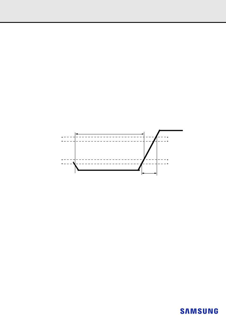
Registered DIMM
datasheet |
Rev. 1.0 |
DDR4 SDRAM |
12.6 CMOS rail to rail Input Levels
12.6.1 CMOS rail to rail Input Levels for RESET_n
[Table 16] CMOS rail to rail Input Levels for RESET_n
Parameter |
Symbol |
Min |
Max |
Unit |
NOTE |
AC Input High Voltage |
VIH(AC)_RESET |
0.8*VDD |
VDD |
V |
6 |
|
|
|
|
|
|
DC Input High Voltage |
VIH(DC)_RESET |
0.7*VDD |
VDD |
V |
2 |
|
|
|
|
|
|
DC Input Low Voltage |
VIL(DC)_RESET |
VSS |
0.3*VDD |
V |
1 |
|
|
|
|
|
|
AC Input Low Voltage |
VIL(AC)_RESET |
VSS |
0.2*VDD |
V |
7 |
|
|
|
|
|
|
Rising time |
TR_RESET |
- |
1.0 |
us |
4 |
|
|
|
|
|
|
RESET pulse width |
tPW_RESET |
1.0 |
- |
us |
3,5 |
|
|
|
|
|
|
NOTE :
1)After RESET_n is registered LOW, RESET_n level shall be maintained below VIL(DC)_RESET during tPW_RESET, otherwise, SDRAM may not be reset.
2)Once RESET_n is registered HIGH, RESET_n level must be maintained above VIH(DC)_RESET, otherwise, SDRAM operation will not be guaranteed until it is reset asserting RESET_n signal LOW.
3)RESET is destructive to data contents.
4)No slope reversal(ringback) requirement during its level transition from Low to High.
5)This definition is applied only “Reset Procedure at Power Stable”.
6)Overshoot might occur. It should be limited by the Absolute Maximum DC Ratings.
7)Undershoot might occur. It should be limited by Absolute Maximum DC Ratings.
tPW_RESET
0.8*VDD
0.7*VDD
0.3*VDD
0.2*VDD
TR_RESET
Figure 10. RESET_n Input Slew Rate Definition
- 25 -
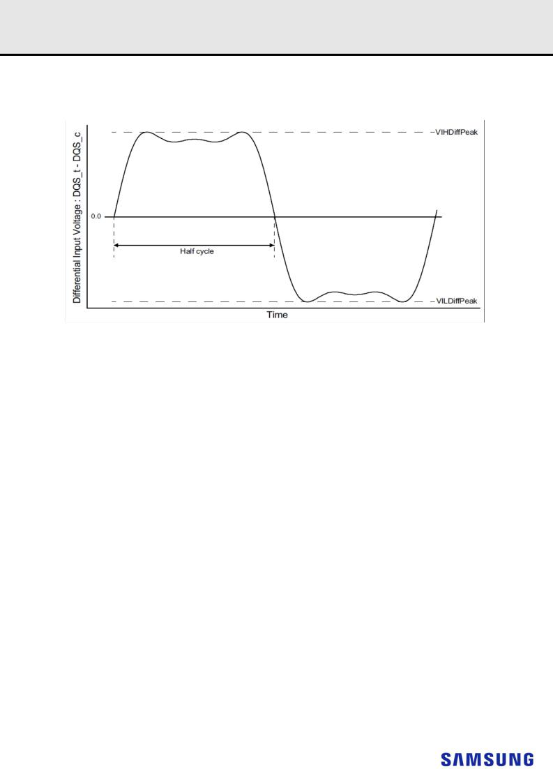
Registered DIMM
datasheet |
Rev. 1.0 |
DDR4 SDRAM |
12.7 AC and DC Logic Input Levels for DQS Signals
12.7.1 Differential signal definition
Figure 11. Definition of differential DQS Signal AC-swing Level
12.7.2 Differential swing requirements for DQS (DQS_t - DQS_c)
[Table 17] Differential AC and DC Input Levels for DQS
|
|
DDR4-1600, 1866, |
DDR4-2400 |
DDR4-2666 |
DDR4-2933 |
|
|
|||||
Symbol |
Parameter |
|
2133 |
Unit |
Note |
|||||||
|
|
|
|
|
|
|
||||||
|
|
Min |
|
Max |
Min |
Max |
Min |
Max |
Min |
Max |
|
|
VIHDiffPeak |
VIH.DIFF.Peak Voltage |
186 |
|
Note2 |
160 |
Note2 |
150 |
Note2 |
145 |
Note2 |
mV |
1 |
|
|
|
|
|
|
|
|
|
|
|
|
|
VILDiffPeak |
VIL.DIFF.Peak Voltage |
Note2 |
|
-186 |
Note2 |
-160 |
Note2 |
-150 |
Note2 |
-145 |
mV |
1 |
|
|
|
|
|
|
|
|
|
|
|
|
|
NOTE :
1)Used to define a differential signal slew-rate.
2)These values are not defined; however, the differential signals DQS_t - DQS_c, need to be within the respective limits Overshoot, Undershoot Specification for single-ended signals.
- 26 -
Loading...