


 Loading...
Rev. 1.4. Aug. 2011
M471B5773DH0
M471B5273DH0
204pin Unbuffered SODIMM
based on 2Gb D-die
78FBGA with Lead-Free & Halogen-Free (RoHS compliant)
datasheet
SAMSUNG ELECTRONICS RESERVES THE RIGHT TO CHANGE PRODUCTS, INFORMATION AND
SPECIFICATIONS WITHOUT NOTICE.
Products and specifications discussed herein are for reference purposes only. All information discussed herein is provided on an "AS IS" basis, without warranties of any kind.
This document and all information discussed herein remain the sole and exclusive property of Samsung Electronics. No license of any patent, copyright, mask work, trademark or any other intellectual property right is granted by one party to the other party under this document, by implication, estoppel or otherwise.
Samsung products are not intended for use in life support, critical care, medical, safety equipment, or similar applications where product failure could result in loss of life or personal or physical harm, or any military or defense application, or any governmental procurement to which special terms or provisions may apply.
For updates or additional information about Samsung products, contact your nearest Samsung office.
All brand names, trademarks and registered trademarks belong to their respective owners.
2011 Samsung Electronics Co., Ltd. All rights reserved.
- 1 -

Unbuffered SODIMM
datasheet
Rev. 1.4
DDR3 SDRAM
Revision History
Revision No. |
History |
Draft Date |
Remark |
Editor |
1.0 |
- First Release |
Aug. 2010 |
- |
S.H.Kim |
1.01 |
- Changed note comment on page. 27, 35 |
Aug. 2010 |
- |
S.H.Kim |
1.1 |
- Corrected IDD current spec.(IDD7) |
Sep. 2010 |
- |
S.H.Kim |
1.2 |
- Changed Input/Output capacitance on page 21. |
Sep. 2010 |
- |
S.H.Kim |
1.3 |
- Changed 1866 speed bin table on page 26. |
Nov. 2010 |
- |
S.H.Kim |
1.31 |
- Corrected typo. |
Dec. 2010 |
- |
S.H.Kim |
1.32 |
- Corrected typo. |
May. 2011 |
- |
J.Y.Lee |
1.33 |
- Corrected typo. |
Jul. 2011 |
- |
J.Y.Lee |
1.4 |
- Changed timing parameters (Setup/Hold time) |
Aug. 2011 |
- |
J.Y.Lee |
- 2 -
Unbuffered SODIMM
datasheet
Rev. 1.4
DDR3 SDRAM
Table Of Contents |
|
|
204pin Unbuffered SODIMM based on 2Gb D-die |
|
|
1. DDR3 Unbuffered SODIMM Ordering Information........................................................................................................ |
4 |
|
2. Key Features................................................................................................................................................................. |
4 |
|
3. Address Configuration .................................................................................................................................................. |
4 |
|
4. x64 DIMM Pin Configurations (Front side/Back Side)................................................................................................... |
5 |
|
5. Pin Description ............................................................................................................................................................. |
6 |
|
6. Input/Output Functional Description.............................................................................................................................. |
7 |
|
7. Function Block Diagram:............................................................................................................................................... |
8 |
|
7.1 2GB, 256Mx64 Module (Populated as 1 rank of x8 DDR3 SDRAMs) ..................................................................... |
8 |
|
7.2 4GB, 512Mx64 Module (Populated as 2 ranks of x8 DDR3 SDRAMs) ................................................................... |
9 |
|
8. Absolute Maximum Ratings .......................................................................................................................................... |
10 |
|
8.1 Absolute Maximum DC Ratings............................................................................................................................... |
10 |
|
8.2 DRAM Component Operating Temperature Range ................................................................................................ |
10 |
|
9. AC & DC Operating Conditions..................................................................................................................................... |
10 |
|
9.1 Recommended DC Operating Conditions (SSTL-15).............................................................................................. |
10 |
|
10. AC & DC Input Measurement Levels .......................................................................................................................... |
11 |
|
10.1 |
AC & DC Logic Input Levels for Single-ended Signals.......................................................................................... |
11 |
10.2 |
VREF Tolerances.................................................................................................................................................... |
12 |
10.3 |
AC and DC Logic Input Levels for Differential Signals .......................................................................................... |
13 |
10.3.1. Differential Signals Definition ......................................................................................................................... |
13 |
|
10.3.2. Differential Swing Requirement for Clock (CK-CK) and Strobe (DQS-DQS) ................................................ |
13 |
|
10.3.3. Single-ended Requirements for Differential Signals ...................................................................................... |
14 |
|
10.3.4. Differential Input Cross Point Voltage ............................................................................................................ |
15 |
|
10.4 |
Slew Rate Definition for Single Ended Input Signals............................................................................................. |
15 |
10.5 |
Slew rate definition for Differential Input Signals ................................................................................................... |
15 |
11. AC & DC Output Measurement Levels ....................................................................................................................... |
16 |
|
11.1 |
Single Ended AC and DC Output Levels............................................................................................................... |
16 |
11.2 |
Differential AC and DC Output Levels ................................................................................................................... |
16 |
11.3 |
Single-ended Output Slew Rate ............................................................................................................................ |
16 |
11.4 |
Differential Output Slew Rate ................................................................................................................................ |
17 |
12. DIMM IDD specification definition ............................................................................................................................... |
18 |
|
13. IDD SPEC Table ......................................................................................................................................................... |
20 |
|
14. Input/Output Capacitance ........................................................................................................................................... |
21 |
|
15. Electrical Characteristics and AC timing ..................................................................................................................... |
22 |
|
15.1 |
Refresh Parameters by Device Density................................................................................................................. |
22 |
15.2 |
Speed Bins and CL, tRCD, tRP, tRC and tRAS for Corresponding Bin ................................................................ |
22 |
15.3 |
Speed Bins and CL, tRCD, tRP, tRC and tRAS for corresponding Bin ................................................................. |
22 |
15.3.1. Speed Bin Table Notes .................................................................................................................................. |
27 |
|
16. Timing Parameters by Speed Grade .......................................................................................................................... |
28 |
|
16.1 |
Jitter Notes ............................................................................................................................................................ |
34 |
16.2 |
Timing Parameter Notes........................................................................................................................................ |
35 |
17. Physical Dimensions :................................................................................................................................................. |
36 |
|
17.1 |
256Mbx8 based 256Mx64 Module (1 Rank) - M471B5773DH0............................................................................ |
36 |
17.2 |
256Mbx8 based 512Mx64 Module (2 Ranks) - M471B5273DH0 .......................................................................... |
37 |
- 3 -

Unbuffered SODIMM
datasheet
Rev. 1.4
DDR3 SDRAM
1. DDR3 Unbuffered SODIMM Ordering Information
Part Number2 |
Density |
Organization |
Component Composition |
Number of |
Height |
|
Rank |
||||||
|
|
|
|
|
||
M471B5773DH0-CF8/H9/K0/MA |
2GB |
256Mx64 |
256Mx8(K4B2G0846D-HC##)*8 |
1 |
30mm |
|
|
|
|
|
|
|
|
M471B5273DH0-CF8/H9/K0/MA |
4GB |
512Mx64 |
256Mx8(K4B2G0846D-HC##)*16 |
2 |
30mm |
|
|
|
|
|
|
|
NOTE :
1."##" - F8/H9/K0/MA
2.F8 - 1066Mbps 7-7-7 / H9 - 1333Mbps 9-9-9 / K0 - 1600Mbps 11-11-11 / MA - 1866Mbps 13-13-13
-DDR3-1866(13-13-13) is backward compatible to DDR3-1600(11-11-11), DDR3-1333(9-9-9), DDR3-1066(7-7-7)
-DDR3-1600(11-11-11) is backward compatible to DDR3-1333(9-9-9), DDR3-1066(7-7-7)
-DDR3-1333(9-9-9) is backward compatible to DDR3-1066(7-7-7)
2. Key Features
Speed |
DDR3-800 |
DDR3-1066 |
DDR3-1333 |
DDR3-1600 |
DDR3-1866 |
Unit |
|
6-6-6 |
7-7-7 |
9-9-9 |
11-11-11 |
13-13-13 |
|||
|
|
||||||
tCK(min) |
2.5 |
1.875 |
1.5 |
1.25 |
1.07 |
ns |
|
|
|
|
|
|
|
|
|
CAS Latency |
6 |
7 |
9 |
11 |
13 |
tCK |
|
|
|
|
|
|
|
|
|
tRCD(min) |
15 |
13.125 |
13.5 |
13.75 |
13.91 |
ns |
|
|
|
|
|
|
|
|
|
tRP(min) |
15 |
13.125 |
13.5 |
13.75 |
13.91 |
ns |
|
|
|
|
|
|
|
|
|
tRAS(min) |
37.5 |
37.5 |
36 |
35 |
34 |
ns |
|
|
|
|
|
|
|
|
|
tRC(min) |
52.5 |
50.625 |
49.5 |
48.75 |
47.91 |
ns |
|
|
|
|
|
|
|
|
•JEDEC standard 1.5V ± 0.075V Power Supply
•VDDQ = 1.5V ± 0.075V
•400MHz fCK for 800Mb/sec/pin, 533MHz fCK for 1066Mb/sec/pin, 667MHz fCK for 1333Mb/sec/pin, 800MHz fCK for 1600Mb/sec/pin, 933MHz fCK for 1866Mb/sec/pin
•8 independent internal bank
•Programmable CAS Latency: 5,6,7,8,9,10,11,13
•Programmable Additive Latency(Posted CAS) : 0, CL - 2, or CL - 1 clock
•Programmable CAS Write Latency(CWL) = 5 (DDR3-800), 6 (DDR3-1066), 7 (DDR3-1333), 8 (DDR3-1600) and 9 (DDR3-1866)
•Burst Length: 8 (Interleave without any limit, sequential with starting address “000” only), 4 with tCCD = 4 which does not allow seamless read or write [either On the fly using A12 or MRS]
•Bi-directional Differential Data Strobe
•On Die Termination using ODT pin
•Average Refresh Period 7.8us at lower then TCASE 85°C, 3.9us at 85°C < TCASE ≤ 95°C
•Asynchronous Reset
3. Address Configuration
Organization |
Row Address |
Column Address |
Bank Address |
Auto Precharge |
256Mx8(2Gb) based Module |
A0-A14 |
A0-A9 |
BA0-BA2 |
A10/AP |
|
|
|
|
|
- 4 -

Unbuffered SODIMM
datasheet
Rev. 1.4
DDR3 SDRAM
4. x64 DIMM Pin Configurations (Front side/Back Side)
Pin |
Front |
Pin |
|
Back |
|
Pin |
Front |
|
Pin |
Back |
Pin |
Front |
Pin |
Back |
||||||||||||||||||||||||||
1 |
VREFDQ |
2 |
|
|
VSS |
|
71 |
|
|
|
VSS |
|
72 |
|
|
VSS |
139 |
|
VSS |
140 |
|
DQ38 |
||||||||||||||||||
3 |
|
VSS |
4 |
|
|
DQ4 |
|
|
|
|
|
|
|
|
|
|
|
|
|
|
KEY |
|
|
|
|
|
|
|
141 |
|
DQ34 |
142 |
|
DQ39 |
||||||
5 |
|
DQ0 |
6 |
|
|
DQ5 |
|
73 |
|
CKE0 |
|
74 |
CKE1 |
143 |
|
DQ35 |
144 |
|
VSS |
|||||||||||||||||||||
7 |
|
DQ1 |
8 |
|
|
VSS |
|
75 |
|
|
|
VDD |
|
76 |
|
|
VDD |
145 |
|
VSS |
146 |
|
DQ44 |
|||||||||||||||||
9 |
|
VSS |
10 |
|
|
|
|
|
77 |
|
|
|
|
NC |
|
78 |
A153 |
147 |
|
DQ40 |
148 |
|
DQ45 |
|||||||||||||||||
DQS0 |
||||||||||||||||||||||||||||||||||||||||
11 |
|
DM0 |
12 |
|
DQS0 |
|
79 |
|
|
|
BA2 |
|
80 |
A143 |
149 |
|
DQ41 |
150 |
|
VSS |
||||||||||||||||||||
13 |
|
VSS |
14 |
|
|
VSS |
|
81 |
|
|
|
VDD |
|
82 |
|
|
VDD |
151 |
|
VSS |
152 |
|
|
|
|
|||||||||||||||
|
|
DQS5 |
||||||||||||||||||||||||||||||||||||||
15 |
|
DQ2 |
16 |
|
|
DQ6 |
|
83 |
|
|
|
|
|
|
|
|
|
|
|
|
|
84 |
|
|
A11 |
153 |
|
DM5 |
154 |
|
DQS5 |
|||||||||
|
A12/BC |
|
|
|
|
|
|
|||||||||||||||||||||||||||||||||
|
|
|
|
|
|
|
|
|
|
|
|
|
|
|
|
|
|
|
|
|
|
|
|
|
|
|||||||||||||||
17 |
|
DQ3 |
18 |
|
|
DQ7 |
|
85 |
|
|
|
|
A9 |
|
86 |
|
|
|
A7 |
155 |
|
VSS |
156 |
|
VSS |
|||||||||||||||
19 |
|
VSS |
20 |
|
|
VSS |
|
87 |
|
|
|
VDD |
|
88 |
|
|
VDD |
157 |
|
DQ42 |
158 |
|
DQ46 |
|||||||||||||||||
21 |
|
DQ8 |
22 |
|
|
DQ12 |
|
89 |
|
|
|
|
A8 |
|
90 |
|
|
A6 |
159 |
|
DQ43 |
160 |
|
DQ47 |
||||||||||||||||
|
|
|
|
|
|
|
|
|
|
|
|
|
|
|
|
|
|
|
|
|
|
|
|
|
||||||||||||||||
23 |
|
DQ9 |
24 |
|
|
DQ13 |
|
91 |
|
|
|
|
A5 |
|
92 |
|
|
A4 |
161 |
|
VSS |
162 |
|
VSS |
||||||||||||||||
25 |
|
VSS |
26 |
|
|
VSS |
|
93 |
|
|
|
VDD |
|
94 |
|
|
VDD |
163 |
|
DQ48 |
164 |
|
DQ52 |
|||||||||||||||||
27 |
|
|
|
28 |
|
|
DM1 |
|
95 |
|
|
|
|
A3 |
|
96 |
|
|
A2 |
165 |
|
DQ49 |
166 |
|
DQ53 |
|||||||||||||||
DQS1 |
|
|
||||||||||||||||||||||||||||||||||||||
29 |
|
DQS1 |
30 |
|
|
|
|
|
97 |
|
|
|
|
A1 |
|
98 |
|
|
A0 |
167 |
|
VSS |
168 |
|
VSS |
|||||||||||||||
|
RESET |
|
||||||||||||||||||||||||||||||||||||||
31 |
|
VSS |
32 |
|
|
VSS |
|
99 |
|
|
|
VDD |
|
100 |
|
|
VDD |
169 |
|
|
|
170 |
|
DM6 |
||||||||||||||||
|
|
|
|
|
|
DQS6 |
|
|||||||||||||||||||||||||||||||||
33 |
|
DQ10 |
34 |
|
|
DQ14 |
|
101 |
|
|
|
CK0 |
|
102 |
|
CK1 |
171 |
|
DQS6 |
172 |
|
VSS |
||||||||||||||||||
35 |
|
DQ11 |
36 |
|
|
DQ15 |
|
103 |
|
|
|
|
|
|
|
|
|
|
|
|
|
104 |
|
|
|
|
|
|
|
173 |
|
VSS |
174 |
|
DQ54 |
|||||
|
|
CK0 |
CK1 |
|
|
|||||||||||||||||||||||||||||||||||
37 |
|
VSS |
38 |
|
|
VSS |
|
105 |
|
|
|
VDD |
|
106 |
|
|
VDD |
175 |
|
DQ50 |
176 |
|
DQ55 |
|||||||||||||||||
39 |
|
DQ16 |
40 |
|
|
DQ20 |
|
107 |
A10/AP |
|
108 |
|
|
BA1 |
177 |
|
DQ51 |
178 |
|
VSS |
||||||||||||||||||||
41 |
|
DQ17 |
42 |
|
|
DQ21 |
|
109 |
|
|
|
BA0 |
|
110 |
|
|
|
|
|
|
|
179 |
|
VSS |
180 |
|
DQ60 |
|||||||||||||
|
|
|
|
|
|
RAS |
|
|
||||||||||||||||||||||||||||||||
43 |
|
VSS |
44 |
|
|
VSS |
|
111 |
|
|
|
VDD |
|
112 |
|
|
VDD |
181 |
|
DQ56 |
182 |
|
DQ61 |
|||||||||||||||||
45 |
|
|
|
46 |
|
|
DM2 |
|
113 |
|
|
|
|
|
|
|
|
|
|
|
|
114 |
|
|
|
|
|
|
|
183 |
|
DQ57 |
184 |
|
VSS |
|||||
DQS2 |
|
|
|
|
WE |
|
|
S0 |
|
|
||||||||||||||||||||||||||||||
47 |
|
DQS2 |
48 |
|
|
VSS |
|
115 |
|
|
|
|
|
|
|
|
|
|
|
|
116 |
ODT0 |
185 |
|
VSS |
186 |
|
|
|
|||||||||||
|
|
|
|
CAS |
|
|
DQS7 |
|||||||||||||||||||||||||||||||||
49 |
|
VSS |
50 |
|
|
DQ22 |
|
117 |
|
|
|
VDD |
|
118 |
|
|
VDD |
187 |
|
DM7 |
188 |
|
DQS7 |
|||||||||||||||||
50 |
|
DQ18 |
52 |
|
|
DQ23 |
|
119 |
|
A133 |
|
120 |
ODT1 |
189 |
|
VSS |
190 |
|
VSS |
|||||||||||||||||||||
53 |
|
DQ19 |
54 |
|
|
VSS |
|
121 |
|
|
|
|
|
|
|
|
|
|
|
|
|
122 |
|
|
NC |
191 |
|
DQ58 |
192 |
|
DQ62 |
|||||||||
|
|
|
|
|
|
S1 |
|
|
|
|
||||||||||||||||||||||||||||||
55 |
|
VSS |
56 |
|
|
DQ28 |
|
123 |
|
|
|
VDD |
|
124 |
|
|
VDD |
193 |
|
DQ59 |
194 |
|
DQ63 |
|||||||||||||||||
57 |
|
DQ24 |
58 |
|
|
DQ29 |
|
125 |
|
TEST |
|
126 |
VREFCA |
195 |
|
VSS |
196 |
|
VSS |
|||||||||||||||||||||
59 |
|
DQ25 |
60 |
|
|
VSS |
|
127 |
|
|
|
VSS |
|
128 |
|
|
VSS |
197 |
|
SA0 |
198 |
|
NC |
|||||||||||||||||
61 |
|
VSS |
62 |
|
|
|
|
|
129 |
|
DQ32 |
|
130 |
DQ36 |
199 |
VDDSPD |
200 |
|
SDA |
|||||||||||||||||||||
|
DQS3 |
|
||||||||||||||||||||||||||||||||||||||
63 |
|
DM3 |
64 |
|
DQS3 |
|
131 |
|
DQ33 |
|
132 |
DQ37 |
201 |
|
SA1 |
202 |
|
SCL |
||||||||||||||||||||||
|
|
|
|
|
|
|
|
|
|
|
|
|
|
|
|
|
|
|
|
|
|
|
|
|||||||||||||||||
65 |
|
VSS |
66 |
|
|
VSS |
|
133 |
|
|
|
VSS |
|
134 |
|
|
VSS |
203 |
|
VTT |
204 |
|
VTT |
|||||||||||||||||
67 |
|
DQ26 |
68 |
|
|
DQ30 |
|
135 |
|
|
|
|
|
|
|
|
|
|
|
136 |
DM4 |
|
|
|
|
|
|
|
|
|
||||||||||
|
|
|
DQS4 |
|
|
|
|
|
|
|
|
|
||||||||||||||||||||||||||||
|
|
|
|
|
|
|
|
|
|
|
|
|
|
|
|
|
|
|
|
|
|
|
|
|
||||||||||||||||
69 |
|
DQ27 |
70 |
|
|
DQ31 |
|
137 |
|
DQS4 |
|
138 |
|
|
VSS |
|
|
|
|
|
|
|
|
|
||||||||||||||||
NOTE :
1.NC = No Connect, NU = Not Usable, RFU = Reserved Future Use
2.TEST(pin 125) is reserved for bus analysis probes and is NC on normal memory modules.
3.This address might be connected to NC balls of the DRAMs (depending on density); either way they will be connected to the termination resistor.
SAMSUNG ELECTRONICS CO., Ltd. reserves the right to change products and specifications without notice.
- 5 -

Unbuffered SODIMM
datasheet
Rev. 1.4
DDR3 SDRAM
5. Pin Description
Pin Name |
Description |
Number |
|
Pin Name |
Description |
Number |
|||||||||||||||
|
CK0, CK1 |
Clock Inputs, positive line |
2 |
|
DQ0-DQ63 |
Data Input/Output |
64 |
||||||||||||||
|
|
|
|
|
|
|
|
|
|
|
|
|
|
|
|
|
|
|
|
|
|
|
|
|
|
|
|
|
|
|
|
|
|
|
|
|
|
|
|
|
|
Data Masks/ Data strobes, |
8 |
|
CK0, CK1 |
Clock Inputs, negative line |
2 |
|
DM0-DM7 |
||||||||||||||||
|
|
Termination data strobes |
|||||||||||||||||||
|
|
|
|
|
|
|
|
|
|
|
|
|
|
|
|
|
|
|
|
|
|
|
|
|
|
|
|
||||||||||||||||
CKE0, CKE1 |
Clock Enables |
2 |
DQS0-DQS7 |
Data strobes |
8 |
||||||||||||||||
|
|
|
|
|
|
|
|
|
|
|
|
|
|
|
|
|
|
|
|
|
|
|
|
|
|
|
|
|
|
|
|
|
Row Address Strobe |
1 |
|
|
|
- |
|
|
|
Data strobes complement |
8 |
|
|
|
RAS |
DQS0 |
DQS7 |
||||||||||||||||
|
|
|
|
|
|
|
|
|
|
|
|
|
|
|
|
|
|
||||
|
|
|
|
|
|
|
|
|
|
|
Column Address Strobe |
1 |
|
|
|
|
|
|
Reset Pin |
1 |
|
|
|
|
CAS |
|
RESET |
||||||||||||||||
|
|
|
|
|
|
|
|
|
|
|
Write Enable |
1 |
|
|
TEST |
Logic Analyzer specific test pin (No connect |
1 |
||||
|
|
|
|
WE |
|
|
|||||||||||||||
|
|
|
|
|
|
on SODIMM) |
|||||||||||||||
|
|
|
|
|
|
|
|
|
|
|
|
|
|
|
|
|
|
|
|
|
|
|
|
|
|
|
|
|
|
|
|
|
|
|
|||||||||
|
|
|
|
|
|
|
|
|
|
|
Chip Selects |
2 |
|
|
VDD |
Core and I/O Power |
18 |
||||
|
|
S0, S1 |
|
|
|||||||||||||||||
A0-A9, A11, |
Address Inputs |
14 |
|
|
VSS |
Ground |
52 |
||||||||||||||
|
A13-A15 |
|
|
||||||||||||||||||
|
|
|
|
|
|
|
|
|
|
|
|
||||||||||
|
|
|
|
|
|
|
|
|
|
|
|
|
|
|
|
|
|||||
|
A10/AP |
Address Input/Autoprecharge |
1 |
|
VREFDQ |
Input/Output Reference |
2 |
||||||||||||||
|
|
VREFCA |
|||||||||||||||||||
|
|
|
|
|
|
|
|
|
|
|
|
|
|
|
|
||||||
|
|
|
|
|
|
|
|
|
|
|
Address Input/Burst chop |
1 |
|
VDDSPD |
SPD and Temp sensor Power |
1 |
|||||
|
A12/BC |
|
|||||||||||||||||||
|
BA0-BA2 |
SDRAM Bank Addresses |
3 |
|
|
VTT |
Termination Voltage |
2 |
|||||||||||||
ODT0, ODT1 |
On-die termination control |
2 |
|
|
|
NC |
Reserved for future use |
3 |
|||||||||||||
|
|
|
|
|
|
|
|
|
|
|
|
|
|
|
|||||||
|
|
|
SCL |
Serial Presence Detect (SPD) Clock Input |
1 |
|
|
|
|
|
|
|
Total |
204 |
|||||||
|
|
|
|
|
|
|
|
|
|
|
|
|
|
|
|||||||
|
|
|
SDA |
SPD Data Input/Output |
1 |
|
|
|
|
|
|
|
|
|
|||||||
|
|
|
|
|
|
|
|
|
|
|
|
|
|||||||||
|
SA0-SA1 |
SPD Address |
2 |
|
|
|
|
|
|
|
|
|
|||||||||
|
|
|
|
|
|
|
|
|
|
|
|
|
|
|
|
|
|
|
|
|
|
NOTE:
*The VDD and VDDQ pins are tied common to a single power-plane on these designs.
- 6 -

Unbuffered SODIMM
datasheet
Rev. 1.4
DDR3 SDRAM
6. Input/Output Functional Description
|
Symbol |
|
Type |
|
|
Function |
||||||||||||||||||
|
CK0-CK1 |
|
|
|
The system clock inputs. All address and command lines are sampled on the cross point of the rising edge of CK and |
|||||||||||||||||||
|
|
Input |
|
falling edge of CK. A Delay Locked Loop (DLL) circuit is driven from the clock inputs and output timing for read opera- |
||||||||||||||||||||
|
CK0-CK1 |
|
|
|||||||||||||||||||||
|
|
|
|
tions is synchronized to the input clock. |
||||||||||||||||||||
|
|
|
|
|
|
|
|
|
|
|
|
|
|
|
||||||||||
|
|
|
|
|
|
|
|
|
|
|
|
|
|
|
|
|||||||||
|
CKE0-CKE1 |
|
Input |
|
Activates the DDR3 SDRAM CK signal when high and deactivates the CK signal when low. By deactivating the clocks, |
|||||||||||||||||||
|
|
|
CKE low initiates the Power Down mode or the Self Refresh mode. |
|||||||||||||||||||||
|
|
|
|
|
|
|
|
|
|
|
|
|
|
|
||||||||||
|
|
|
|
|
|
|
|
|
|
|
|
|
|
|
|
|||||||||
|
|
|
|
|
|
|
|
|
|
|
|
|
|
|
Enables the associated DDR3 SDRAM command decoder when low and disables the command decoder when high. |
|||||||||
|
|
|
S0-S1 |
|
Input |
|
When the command decoder is disabled, new commands are ignored but previous operations continue. Rank 0 is |
|||||||||||||||||
|
|
|
|
|
|
|
|
|
|
|
|
|
|
|
selected by S0; Rank 1 is selected by S1. |
|||||||||
|
|
|
|
|
|
|
|
|
|
|
|
|
|
|
|
|
|
|
|
|
|
|
|
|
|
|
|
|
|
|
|
|
|
|
|
|
|
|
|
When sampled at the cross point of the rising edge of CK and falling edge of |
|
signals |
|
|
|
and |
|
define |
|
|
|
|
|
|
|
|
|
|
|
|
|
|
|
CK, |
CAS, |
RAS, |
WE |
|||||||
|
RAS, CAS, WE |
|
Input |
|||||||||||||||||||||
|
|
|
the operation to be executed by the SDRAM. |
|||||||||||||||||||||
|
|
|
|
|
|
|
|
|
|
|
|
|
|
|
||||||||||
|
|
|
|
|
||||||||||||||||||||
|
BA0-BA2 |
|
Input |
Selects which DDR3 SDRAM internal bank of eight is activated. |
||||||||||||||||||||
|
|
|
|
|
|
|||||||||||||||||||
|
ODT0-ODT1 |
|
Input |
|
Asserts on-die termination for DQ, DM, DQS, and DQS signals if enabled via the DDR3 SDRAM mode register. |
|||||||||||||||||||
|
|
|
|
|
|
|
|
|
|
|
|
|
|
|
|
|||||||||
|
|
|
|
|
|
|
|
|
|
|
|
|
|
|
During a Bank Activate command cycle, defines the row address when sampled at the cross point of the rising edge of |
|||||||||
|
|
|
|
|
|
|
|
|
|
|
|
|
|
|
CK and falling edge of CK. During a Read or Write command cycle, defines the column address when sampled at the |
|||||||||
|
|
A0-A9, |
|
|
|
cross point of the rising edge of CK and falling edge of CK. In addition to the column address, AP is used to invoke |
||||||||||||||||||
|
A10/AP, |
|
|
|
autoprecharge operation at the end of the burst read or write cycle. If AP is high, autoprecharge is selected and BA0- |
|||||||||||||||||||
|
|
|
|
A11 |
|
Input |
|
BAn defines the bank to be precharged. If AP is low, autoprecharge is disabled. During a Precharge command cycle, |
||||||||||||||||
|
|
|
|
|
|
|
|
AP is used in conjunction with BA0-BAn to control which bank(s) to precharge. If AP is high, all banks will be pre- |
||||||||||||||||
|
A12/BC |
|
|
|||||||||||||||||||||
|
A13-A15 |
|
|
|
charged regardless of the state of BA0-BAn inputs. If AP is low, then BA0-BAn are used to define which bank to pre- |
|||||||||||||||||||
|
|
|
|
|
|
|
|
|
|
|
|
|
|
|
charge.A12(BC) is sampled during READ and WRITE commands to determine if burst chop (on-the fly) will be |
|||||||||
|
|
|
|
|
|
|
|
|
|
|
|
|
|
|
performed (HIGH, no burst chop; LOW, burst chopped) |
|||||||||
|
|
|
|
|
|
|||||||||||||||||||
|
DQ0-DQ63 |
|
I/O |
|
Data Input/Output pins. |
|||||||||||||||||||
|
|
|
|
|
|
|
|
|
|
|
|
|
|
|
|
|||||||||
|
DM0-DM7 |
|
Input |
|
The data write masks, associated with one data byte. In Write mode, DM operates as a byte mask by allowing input |
|||||||||||||||||||
|
|
|
data to be written if it is low but blocks the write operation if it is high. In Read mode, DM lines have no effect. |
|||||||||||||||||||||
|
|
|
|
|
|
|
|
|
|
|
|
|
|
|
||||||||||
|
|
|
|
|
|
|
|
|
|
|
|
|
|
|
|
|||||||||
|
DQS0-DQS7 |
|
|
|
The data strobes, associated with one data byte, sourced with data transfers. In Write mode, the data strobe is |
|||||||||||||||||||
|
|
I/O |
|
sourced by the controller and is centered in the data window. In Read mode, the data strobe is sourced by the DDR3 |
||||||||||||||||||||
|
DQS0-DQS7 |
|
|
SDRAMs and is sent at the leading edge of the data window. DQS signals are complements, and timing is relative to |
||||||||||||||||||||
|
|
|
|
|||||||||||||||||||||
|
|
|
|
|
|
|
|
|
|
|
|
|
|
|
the crosspoint of respective DQS and DQS. |
|||||||||
|
|
|
|
|
|
|
|
|
|
|
|
|
|
|
||||||||||
|
VDD,VDDSPD, |
|
Supply |
Power supplies for core, I/O, Serial Presence Detect, Temp sensor, and ground for the module. |
||||||||||||||||||||
|
|
|
|
VSS |
|
|||||||||||||||||||
|
|
|
|
|
|
|
|
|
|
|
|
|
|
|
|
|
||||||||
|
VREFDQ, |
|
Supply |
Reference voltage for SSTL15 inputs. |
||||||||||||||||||||
|
VREFCA |
|
||||||||||||||||||||||
|
|
|
|
|
|
|
|
|
|
|
|
|
|
|||||||||||
|
|
|
|
SDA |
|
I/O |
|
This is a bidirectional pin used to transfer data into or out of the SPD EEPROM and Temp sensor. A resistor must be |
||||||||||||||||
|
|
|
|
|
|
connected from the SDA bus line to VDDSPD on the system planar to act as a pull up. |
||||||||||||||||||
|
|
|
|
|
|
|
|
|
|
|
|
|
|
|
||||||||||
|
|
|
|
SCL |
|
Input |
|
This signal is used to clock data into and out of the SPD EEPROM and Temp sensor. |
||||||||||||||||
|
|
|
|
|
||||||||||||||||||||
|
SA0-SA1 |
|
Input |
Address pins used to select the Serial Presence Detect and Temp sensor base address. |
||||||||||||||||||||
|
|
|
|
|
|
|
|
|||||||||||||||||
|
|
|
TEST |
|
I/O |
|
The TEST pin is reserved for bus analysis tools and is not connected on normal memory modules |
|||||||||||||||||
|
|
|
|
|
|
|
|
|
||||||||||||||||
|
|
|
|
|
|
|
|
|
|
|
|
Input |
|
|
In Active Low This signal resets the DDR3 SDRAM |
|||||||||
|
|
RESET |
RESET |
|||||||||||||||||||||
|
|
|
|
|
|
|
|
|
|
|
|
|
|
|
|
|
|
|
|
|
|
|
|
|
- 7 -

Unbuffered SODIMM
datasheet
Rev. 1.4
DDR3 SDRAM
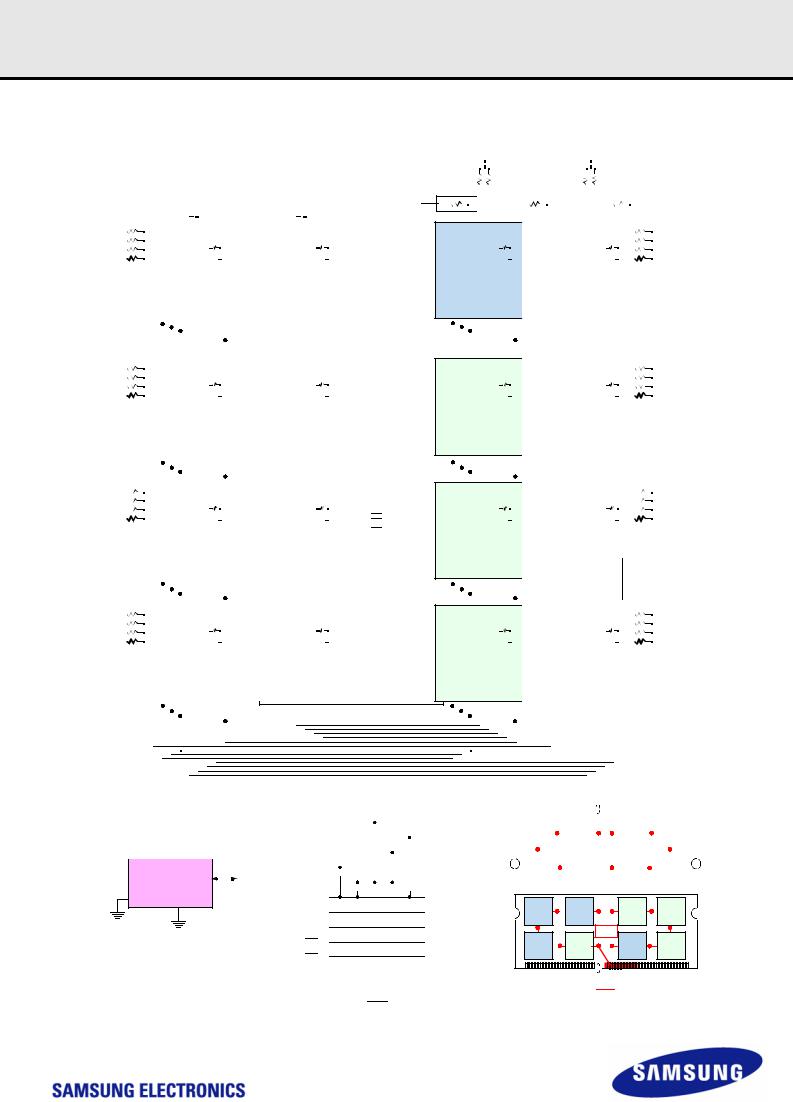
7. Function Block Diagram:
7.1 2GB, 256Mx64 Module (Populated as 1 rank of x8 DDR3 SDRAMs)
|
|
|
|
S0 |
|
RAS |
|
CAS |
|
WE CK0 |
|
CK0 CKE0 ODT0 A[0:N] /BA[0:N] |
|
|
|
|
|
|
|
|
|
|
|
|
|
|
|
|
|
|
|
|
|
|
||||||||||||||||
|
|
|
|
|
|
|
|
|
|
|
|
|
|
|
|
|
|
|
|
|
|
|
|
|
|
|
|
|
|
|||||||||||||||||||||
|
|
|
|
|
|
|
|
|
|
|
|
|
|
|
|
|
|
|
|
|
|
|
|
|
|
|||||||||||||||||||||||||
|
|
|
|
|
|
|
|
|
|
|
|
|
|
|
|
|
|
|
|
|
|
|
|
|
|
|
|
|
|
|
|
|
|
|
|
|
|
|
|
|
|
|
|
|
|
|
|
|
|
|
DQS0 |
|
|
DQS |
240Ω |
|
|
|
DQS1 |
|
|
DQS |
|
240Ω |
|||||||||||||||||||||||||||||||||||||
DQS0 |
|
|
DQS |
± 1% |
|
|
|
DQS1 |
|
|
DQS |
± 1% |
|
|
||||||||||||||||||||||||||||||||||||
|
|
|
|
|
||||||||||||||||||||||||||||||||||||||||||||||
DM0 |
|
|
DM |
|
|
|
|
|
|
ZQ |
|
|
|
DM1 |
|
|
DM |
|
|
|
|
ZQ |
|
|
||||||||||||||||||||||||||
|
|
|
|
|
|
|
|
|
|
|||||||||||||||||||||||||||||||||||||||||
DQ[0:7] |
|
|
DQ[0:7] |
|
|
|
|
|
|
|
|
|
|
|
DQ[8:15] |
|
|
DQ[0:7] |
|
|
|
|
|
|
|
|
|
|||||||||||||||||||||||
|
|
|
|
|
|
|
|
|
|
|
|
|
|
|
|
|
|
D0 |
|
|
|
|
|
|
|
|
|
|
|
|
|
|
|
|
D4 |
|||||||||||||||
|
|
|
|
CS |
|
RAS |
|
CAS |
|
WE CK |
|
CK CKE ODT |
A[0:N]/BA[0:N] |
|
|
|
|
|
CS |
|
RAS |
|
CAS |
|
WE CK |
|
CK CKE ODT A[0:N]/BA[0:N] |
|||||||||||||||||||||||
|
|
|
|
|
|
|
|
|
|
|
|
|
|
|
|
|
||||||||||||||||||||||||||||||||||
|
|
|
|
|
|
|
|
|
|
|
|
|
|
|
|
|
|
|
|
|
|
|
|
|
|
|
|
|
|
|
|
|
|
|
|
|
|
|
|
|
|
|
|
|
|
|
|
|
|
|
|
|
|
|
|
|
|
|
|
|
|
|
|
|
|
|
|
|
|
|
|
|
|
|
|
|
|
|
|
|
|
|
|
|
|
|
|
|
|
|
|
|
|
|
|
|
|
|
|
|
|
|
|
|
|
|
|
|
|
|
|
|
|
|
|
|
|
|
|
|
|
|
|
|
|
|
|
|
|
|
|
|
|
|
|
|
|
|
|
|
|
|
|
|
|
|
|
|
|
|
|
|
|
|
|
|
|
|
|
|
|
|
|
|
|
|
|
|
|
|
|
|
|
|
|
|
|
|
|
|
|
|
|
|
|
|
|
|
|
|
|
|
|
|
|
|
|
|
|
|
|
|
|
|
|
|
|
|
|
|
|
|
|
|
|
|
|
|
|
|
|
|
|
|
|
|
|
|
|
|
|
|
|
|
|
|
|
|
|
|
|
|
|
|
|
|
|
|
|
|
|
|
|
|
|
|
|
|
|
|
|
|
|
|
|
|
|
|
|
|
|
|
|
|
|
|
|
|
|
|
|
|
|
|
|
|
|
|
|
|
|
|
|
|
|
|
|
|
|
|
|
|
|
|
|
|
|
|
|
|
|
|
|
|
|
|
|
|
|
|
|
|
|
|
|
|
|
|
|
|
|
|
|
|
|
|
|
|
|
|
|
|
|
|
|
|
|
|
|
|
|
|
|
|
|
|
|
|
|
|
|
|
|
|
|
|
|
|
|
|
|
|
|
|
|
|
|
|
|
|
|
|
|
|
|
|
|
|
|
|
|
|
|
|
|
|
|
|
|
|
|
|
|
|
|
|
|
|
|
|
|
|
|
|
|
|
|
|
|
|
|
|
|
|
|
|
|
|
|
|
|
|
|
|
|
|
|
|
|
|
|
|
|
|
|
|
|
|
|
|
|
|
|
|
|
|
|
|
|
|
|
|
|
|
|
|
|
|
|
|
|
|
|
|
|
|
|
|
|
|
|
|
|
|
|
|
|
|
|
|
|
|
|
|
|
|
|
|
|
|
|
|
|
|
|
|
|
|
|
DQS2 |
|
|
DQS |
240Ω |
DQS3 |
|
|
DQS |
240Ω |
|||||||||||||||||||||||||||||
DQS2 |
|
|
DQS |
± 1% |
|
|
|
|
DQS3 |
|
|
DQS |
± 1% |
|
|
|
||||||||||||||||||||||
|
|
|||||||||||||||||||||||||||||||||||||
DM2 |
|
|
DM |
|
|
ZQ |
|
|
|
|
DM3 |
|
|
DM |
|
|
ZQ |
|
|
|
||||||||||||||||||
|
|
|
|
|
|
|||||||||||||||||||||||||||||||||
|
|
|||||||||||||||||||||||||||||||||||||
DQ[16:23] |
|
|
|
DQ[0:7] |
|
|
|
|
|
|
|
|
|
DQ[24:31] |
|
|
|
DQ[0:7] |
|
|
|
|
|
|
|
|
||||||||||||
|
|
|
D1 |
|
|
D5 |
||||||||||||||||||||||||||||||||
|
|
|
|
|
|
|
|
|
|
|
|
|
|
|
|
|
|
|
|
|
|
|||||||||||||||||
|
|
|
|
CS |
|
RAS |
|
CAS |
|
WE CK |
|
CK CKE ODT A[0:N]/BA[0:N] |
|
|
|
|
CS |
|
RAS |
|
CAS |
|
WE CK |
|
CK CKE ODT A[0:N]/BA[0:N] |
|||||||||||||
|
|
|
|
|
|
|
|
|
|
|
|
|
|
|||||||||||||||||||||||||
|
|
|
|
|
|
|
|
|
|
|||||||||||||||||||||||||||||
SCL |
|
|
|
SCL |
|
|
|
|
|
|
|
|
|
|
||
|
|
|
|
|
|
|
|
|
|
|
|
|
||||
SA0 |
|
|
|
A0 |
(SPD) |
|
|
SDA |
||||||||
|
|
|
|
|
||||||||||||
SA1 |
|
|
|
A1 |
|
|
|
|
|
|
|
|
|
|
||
|
|
|
|
|
|
|
|
|
|
|
|
|
||||
|
|
|
|
|
|
A2 |
|
WP |
|
|
|
|||||
|
|
|
|
|
|
|
|
|
||||||||
|
|
|
|
|
|
|
|
|
|
|
|
|
|
|
|
|
|
|
|
|
|
|
|
|
|
|
|
|
|
|
|
|
|
|
|
Vtt |
|
|
|
|
|
|
|
|
|
|
|
|
|
|
|
|
Vtt |
|
|||||
|
|
|
|
|
|
|
|
|
|
|
|
|
|
|
|
|
|||||||||
VDDSPD |
|
|
|
|
|
|
|
|
|
|
|
|
|
|
|
|
SPD |
||||||||
|
|
|
|
|
|
|
|
|
|
|
|
|
|
|
|
||||||||||
VREFCA |
|
|
|
|
|
|
|
|
|
|
|
|
|
|
|
|
D0 |
- D7 |
|||||||
|
|
|
|
|
|
|
|
|
|
|
|
|
|
|
|
||||||||||
VREFDQ |
|
|
|
|
|
|
|
|
|
|
|
|
|
|
|
|
D0 |
- D7 |
|||||||
|
|
|
|
|
|
|
|
|
|
|
|
|
|
|
|
||||||||||
|
VDD |
|
|
|
|
|
|
|
|
|
|
|
|
|
|
|
|
D0 |
- D7 |
||||||
|
|
|
|
|
|
|
|
|
|
|
|
|
|
|
|
|
|||||||||
|
|
|
|
|
|
|
|
|
|
|
|
|
|
|
|
|
|||||||||
|
VSS |
|
|
|
|
|
|
|
|
|
|
|
|
|
|
|
|
D0 |
- D7, SPD |
||||||
|
|
|
|
|
|
|
|
|
|
|
|
|
|
|
|
|
|||||||||
|
CK0 |
|
|
|
|
|
|
|
|
|
|
|
|
|
|
|
|
D0 |
- D7 |
||||||
|
|
|
|
|
|
|
|
|
|
|
|
|
|
|
|
|
|||||||||
|
|
|
|
|
|
|
|
|
|
|
|
|
|
|
|
|
|
|
|
|
D0 |
- D7 |
|||
|
CK0 |
|
|
|
|
|
|
|
|
|
|
|
|
|
|
|
|
||||||||
|
|
|
|
|
|
|
|
|
|
|
|
|
|
|
|
|
|||||||||
|
CK1 |
|
|
|
|
|
|
|
|
|
|
|
|
|
|
|
|
|
|
|
Terminated near |
||||
|
|
|
|
|
|
|
|
|
|
|
|
|
|
|
|
|
|
|
|
||||||
|
|
|
|
|
|
|
|
|
|
|
|
|
|
|
|
|
|
|
|
|
|
|
|
card edge |
|
|
CK1 |
|
|
|
|
|
|
|
|
|
|
|
|
|
|
|
|
NC |
|
||||||
|
|
|
|
|
|
|
|
|
|
|
|
|
|
|
|
|
|
|
|
|
|
||||
|
|
S1 |
|
|
|
|
|
|
|
|
|
|
|
|
|
|
|
|
|
||||||
|
|
|
|
|
|
|
|
|
|
|
|
|
|
|
|
|
|
|
|||||||
ODT1 |
|
|
|
|
|
|
|
|
|
|
|
|
|
|
|
|
NC |
|
|||||||
|
|
|
|
|
|
|
|
|
|
|
|
|
|
|
|
|
|||||||||
CKE1 |
|
|
|
|
|
|
|
|
|
|
|
|
|
|
|
|
NC |
|
|||||||
|
|
|
|
|
|
|
|
|
|
|
|
|
|
|
|
|
|||||||||
|
|
|
|
|
|
|
|
|
|
|
|
|
|
|
|
|
|
D0 |
- D7 |
||||||
RESET |
|
|
|
|
|
|
|
|
|
|
|
|
|
|
|
|
|||||||||
|
|
|
|
|
|
|
|
|
|
|
|
|
|
|
|
|
|||||||||
DQS4 |
|
|
DQS |
240Ω |
|||||||||||||
|
|||||||||||||||||
DQS4 |
|
|
DQS |
± 1% |
|
|
|
||||||||||
|
|||||||||||||||||
DM4 |
|
|
DM |
|
|
ZQ |
|
|
|
||||||||
|
|
|
|
|
|||||||||||||
|
|||||||||||||||||
DQ[32:39] |
|
|
|
DQ[0:7] |
|
|
|
|
|
|
|
||||||
|
|
|
D2 |
||||||||||||||
|
|
|
|
|
|
|
|
|
|
|
|||||||
|
|
|
|
CS |
|
RAS |
|
CAS |
|
WE CK |
|
CK CKE ODT A[0:N]/BA[0:N] |
|||||
|
|
|
|
|
|
|
|||||||||||
|
|
|
|
|
|||||||||||||
|
|
|
|
|
|
|
|
|
|
|
|
|
|
|
|
|
|
|
|
|
|
DQS6 |
|
|
DQS |
|
240Ω |
||||||||||||||||
|
|||||||||||||||||||||
DQS6 |
|
|
DQS |
± 1% |
|
|
|||||||||||||||
|
|||||||||||||||||||||
DM6 |
|
|
DM |
|
|
|
|
ZQ |
|
|
|||||||||||
|
|||||||||||||||||||||
DQ[48:55] |
|
|
DQ[0:7] |
|
|
|
|
|
|
|
|
|
|||||||||
|
|
D3 |
|||||||||||||||||||
|
|
|
|
|
|
|
|
|
|
|
|
|
|||||||||
|
|
|
CS |
|
RAS |
|
CAS |
|
WE CK |
|
CK CKE ODT A[0:N]/BA[0:N] |
||||||||||
|
|
|
|
|
|
|
|||||||||||||||
|
|
|
|
|
|
|
|
|
|
|
|
|
|
|
|
|
|
|
|
|
|
Vtt
VDD
DQS5 |
|
|
DQS |
|
240Ω |
||||||||||||||
|
|||||||||||||||||||
DQS5 |
|
|
DQS |
± 1% |
|
||||||||||||||
|
|||||||||||||||||||
DM5 |
|
|
DM |
|
|
|
|
ZQ |
|
||||||||||
|
|
|
|
||||||||||||||||
DQ[40:47] |
|
|
DQ[0:7] |
|
|
|
|
|
|
|
|||||||||
|
|
D6 |
|||||||||||||||||
|
|
|
|
|
|
|
|
|
|
|
|
|
|||||||
|
|
|
|
CS |
|
RAS |
|
CAS |
|
WE CK |
|
CK CKE ODT A[0:N]/BA[0:N] |
|||||||
|
|
|
|
|
|
|
|
||||||||||||
|
|
|
|
|
|
|
|
|
|
|
|
|
|
|
|
|
|
|
|
|
|
|
|
|
|
|
|
|
|
|
|
|
|
|
|
|
|
|
|
|
|
|
|
|
|
|
|
|
|
|
|
|
|
|
|
|
|
|
|
|
|
|
|
|
|
|
|
|
|
|
|
|
|
|
|
|
|
|
|
|
|
|
|
|
|
|
|
|
|
|
|
|
|
|
|
|
|
|
|
|
|
|
|
|
|
|
|
|
|
|
|
|
|
|
|
|
|
|
|
|
|
|
|
|
|
|
|
|
|
|
|
|
|
|
|
|
|
|
|
|
|
|
|
|
|
|
|
|
|
|
|
|
|
|
|
|
|
|
|
|
|
|
|
|
|
|
|
|
|
|
|
|
|
|
|
|
|
|
|
DQS7 |
|
|
DQS |
|
240Ω |
|||||||||||||||
|
||||||||||||||||||||
DQS7 |
|
|
DQS |
± 1% |
|
|
||||||||||||||
|
||||||||||||||||||||
DM7 |
|
|
DM |
|
|
|
|
ZQ |
|
|
||||||||||
|
|
|
|
|||||||||||||||||
DQ[56:63] |
|
|
DQ[0:7] |
|
|
|
|
|
|
|
|
|||||||||
|
|
D7 |
||||||||||||||||||
|
|
|
|
|
|
|
|
|
|
|
|
|
||||||||
|
|
|
|
CS |
|
RAS |
|
CAS |
|
WE CK |
|
CK CKE ODT A[0:N]/BA[0:N] |
||||||||
|
|
|
|
|
|
|
|
|||||||||||||
|
|
|
|
|
|
|
|
|
|
|
|
|
|
|
|
|
|
|
|
|
|
|
|
|
|
|
|
|
|
|
|
|
|
|
|
|
|
|
|
|
|
|
|
|
|
|
|
|
|
|
|
|
|
|
|
|
|
|
|
|
|
|
|
|
|
|
|
|
|
|
|
|
|
|
|
|
|
|
|
|
|
|
|
|
|
|
|
|
|
|
|
|
|
|
|
|
|
|
|
|
|
|
|
|
|
|
|
|
|
|
|
|
|
|
|
|
|
|
|
|
|
|
|
|
|
|
|
|
|
|
|
|
|
|
|
|
|
|
|
|
|
|
|
|
|
|

 Rank0
Rank0
Vtt
|
|
|
|
|
|
|
V |
|
|
|
|
|
|
|
tt |
V1 |
D4 |
V2 |
D5 |
V3 |
D6 |
V4 |
D7 |
|
|
|
|
V1 |
D0 |
V2 |
D1 |
V3 |
D2 |
V4 |
D3 |
|
|
|
|
||||
|
|
|
|
|
|
|
tt |
|
|
|
|
|
|
|
V |
Address and Controllines
NOTE :
1.DQ wiring may differ from that shown however ,DQ, DM, DQS and DQS relationships are maintained as shown
- 8 -
Unbuffered SODIMM
datasheet
Rev. 1.4
DDR3 SDRAM
7.2 4GB, 512Mx64 Module (Populated as 2 ranks of x8 DDR3 SDRAMs)
|
|
|
S1 |
|
RAS |
|
CAS |
|
WE CK1 |
|
CK1 CKE1 ODT1 A[0:N] /BA[0:N] |
|
S0 |
CK0 |
|
CK0 CKE0 ODT0 |
|
||||||||||||||||||||||||||||||
|
|
|
|
|
|
|
|
|
|
||||||||||||||||||||||||||||||||||||||
|
|
|
|
|
|||||||||||||||||||||||||||||||||||||||||||
|
|
|
|
|
|
|
|
|
|||||||||||||||||||||||||||||||||||||||
|
|
|
|
|
|
|
|
|
|
|
|
|
|
|
|
|
|
|
|
|
|
|
|
|
|
|
|
|
|
|
|
|
|
|
|
|
|
|
|
|
|
|
|
|
|
|
|
|
|
|
|
|
|
|
|
|
|
|
|
|
|
|
|
|
|
|
|
|
|
|
|
|
|
|
|
|
|
|
|
|
|
|
|
|
|
|
|
|
|
|
|
|
|
|
|
DQS3 |
|
|
DQS |
240Ω |
|
|
|
|
|
DQS |
|
240Ω |
|
||||||||||||||||||||||||||||||||||
|
|
|
|
|
|
|
|||||||||||||||||||||||||||||||||||||||||
DQS3 |
|
|
DQS |
± 1% |
|
|
|
|
|
DQS |
± 1% |
|
|||||||||||||||||||||||||||||||||||
|
|
|
|
|
|
|
|||||||||||||||||||||||||||||||||||||||||
DM3 |
|
|
DM |
|
|
|
|
ZQ |
|
|
|
|
|
DM |
|
|
|
|
ZQ |
|
|||||||||||||||||||||||||||
DQ[24:31] |
|
|
DQ[0:7] |
|
|
|
|
|
|
|
|
|
|
|
|
|
DQ[0:7] |
|
|
|
|
|
|
|
|
|
|||||||||||||||||||||
|
|
D11 |
A[N:0]/BA[N:0] |
|
|
D3 |
A[N:0]/BA[N:0] |
||||||||||||||||||||||||||||||||||||||||
|
|
|
|
|
|
|
|
|
|
|
|
|
|
|
|
|
|
|
|
|
|
|
|
|
|
|
|
|
|||||||||||||||||||
|
|
|
CS |
|
RAS |
|
CAS |
|
WE CK |
|
CK CKE ODT |
|
|
|
CS |
|
RAS |
|
CAS |
|
WE CK |
|
CK CKE ODT |
||||||||||||||||||||||||
|
|
|
|
|
|
|
|
|
|
|
|
|
|
||||||||||||||||||||||||||||||||||
|
|
|
|
|
|
|
|
|
|
|
|
|
|
|
|
|
|
|
|
|
|
|
|
|
|
|
|
|
|
|
|
|
|
|
|
|
|
|
|
|
|
|
|
|
|
|
|
|
|
|
|
|
|
|
|
|
|
|
|
|
|
|
|
|
|
|
|
|
|
|
|
|
|
|
|
|
|
|
|
|
|
|
|
|
|
|
|
|
|
|
|
|
|
|
|
|
|
|
|
|
|
|
|
|
|
|
|
|
|
|
|
|
|
|
|
|
|
|
|
|
|
|
|
|
|
|
|
|
|
|
|
|
|
|
|
|
|
|
|
|
|
|
|
|
|
|
|
|
|
|
|
|
|
|
|
|
|
|
|
|
|
|
|
|
|
|
|
|
|
|
|
|
|
|
|
|
|
|
|
|
|
|
|
|
|
|
|
|
|
|
|
DQS1 |
|
|
DQS |
240Ω |
|
|
|
|
|
DQS |
|
240Ω |
|
||||||||||||||||||||||||||||||||||
DQS1 |
|
|
DQS |
± 1% |
|
|
|
|
|
DQS |
± 1% |
|
|||||||||||||||||||||||||||||||||||
DM1 |
|
|
DM |
|
|
|
|
ZQ |
|
|
|
|
|
DM |
|
|
|
|
ZQ |
|
|||||||||||||||||||||||||||
DQ[8:15] |
|
|
DQ[0:7] |
|
|
|
|
|
|
|
|
|
|
|
|
|
DQ[0:7] |
|
|
|
|
|
|
|
|
|
|||||||||||||||||||||
|
|
D1 |
A[N:0]/BA[N:0] |
|
|
|
D9 |
A[N:0]/BA[N:0] |
|||||||||||||||||||||||||||||||||||||||
|
|
|
|
|
|
|
|
|
|
|
|
|
|
|
|
|
|
|
|
|
|
|
|
|
|
|
|
|
|||||||||||||||||||
|
|
|
CS |
|
RAS |
|
CAS |
|
WE CK |
|
CK CKE ODT |
|
|
|
CS |
|
RAS |
|
CAS |
|
WE CK |
|
CK CKE ODT |
||||||||||||||||||||||||
|
|
|
|
|
|
|
|
|
|
|
|
|
|
||||||||||||||||||||||||||||||||||
|
|
|
|
|
|
|
|
|
|
|
|
|
|
|
|
|
|
|
|
|
|
|
|
|
|
|
|
|
|
|
|
|
|
|
|
|
|
|
|
|
|
|
|
|
|
|
|
|
|
|
|
|
|
|
|
|
|
|
|
|
|
|
|
|
|
|
|
|
|
|
|
|
|
|
|
|
|
|
|
|
|
|
|
|
|
|
|
|
|
|
|
|
|
|
|
|
|
|
|
|
|
|
|
|
|
|
|
|
|
|
|
|
|
|
|
|
|
|
|
|
|
|
|
|
|
|
|
|
|
|
|
|
|
|
|
|
|
|
|
|
|
|
|
|
|
|
|
|
|
|
|
|
|
|
|
|
|
|
|
|
|
|
|
|
|
|
|
|
|
|
|
|
|
|
|
|
|
|
|
|
|
|
|
|
|
|
|
|
|
|
|
|
|
|
|
|
|
|
|
|
|
|
|
|
|
|
|
|
|
|
|
|
|
|
|
|
|
|
|
|
|
|
|
|
|
|
|
|
|
|
|
|
|
|
|
||||
DQS0 |
|
|
DQS |
240Ω |
|
|
|
|
|
DQS |
|
240Ω |
|
||||||||||||||||||||||||||||||||||
|
|
|
|
|
|
|
|
||||||||||||||||||||||||||||||||||||||||
DQS0 |
|
|
DQS |
± 1% |
|
|
|
|
|
DQS |
± 1% |
|
|||||||||||||||||||||||||||||||||||
|
|
|
|
|
|
|
|||||||||||||||||||||||||||||||||||||||||
DM0 |
|
|
DM |
|
|
|
|
ZQ |
|
|
|
|
|
DM |
|
|
|
|
ZQ |
|
|||||||||||||||||||||||||||
DQ[0:7] |
|
|
DQ[0:7] |
|
|
|
|
|
|
|
|
|
|
|
|
|
DQ[0:7] |
|
|
|
|
|
|
|
|
|
|||||||||||||||||||||
|
|
D0 |
A[N:0]/BA[N:0] |
|
|
|
D8 |
A[N:0]/BA[N:0] |
|||||||||||||||||||||||||||||||||||||||
|
|
|
|
|
|
|
|
|
|
|
|
|
|
|
|
|
|
|
|
|
|
|
|
|
|
|
|
|
|||||||||||||||||||
|
|
|
CS |
|
RAS |
|
CAS |
|
WE CK |
|
CK CKE ODT |
|
|
|
CS |
|
RAS |
|
CAS |
|
WE CK |
|
CK CKE ODT |
||||||||||||||||||||||||
|
|
|
|
|
|
|
|
|
|
|
|
|
|
||||||||||||||||||||||||||||||||||
|
|
|
|
|
|
|
|
|
|
|
|
|
|
|
|
|
|
|
|
|
|
|
|
|
|
|
|
|
|
|
|
|
|
|
|
|
|
|
|
|
|
|
|
|
|
|
|
|
|
|
|
|
|
|
|
|
|
|
|
|
|
|
|
|
|
|
|
|
|
|
|
|
|
|
|
|
|
|
|
|
|
|
|
|
|
|
|
|
|
|
|
|
|
|
|
|
|
|
|
|
|
|
|
|
|
|
|
|
|
|
|
|
|
|
|
|
|
|
|
|
|
|
|
|
|
|
|
|
|
|
|
|
|
|
|
|
|
|
|
|
|
|
|
|
|
|
|
|
|
|
|
|
|
|
|
|
|
|
|
|
|
|
|
|
|
|
|
|
|
|
|
|
|
|
|
|
|
|
|
|
|
|
|
|
|
|
|
|
|
|
|
|
|
|
|
|
|
|
|
|
|
|
|
|
|
|
|
|
|
|
|
|
|
|
|
|
|
|
|
|
|
|
|
|
|
|
|
|
|
|
|
|
|
|
|
|
|
||
DQS2 |
|
|
DQS |
240Ω |
|
|
|
|
|
DQS |
|
240Ω |
|
||||||||||||||||||||||||||||||||||
|
|
|
|
|
|
|
|
||||||||||||||||||||||||||||||||||||||||
DQS2 |
|
|
DQS |
± 1% |
|
|
|
|
|
DQS |
± 1% |
|
|||||||||||||||||||||||||||||||||||
|
|
|
|
|
|
|
|||||||||||||||||||||||||||||||||||||||||
DM2 |
|
|
DM |
|
|
|
|
ZQ |
|
|
|
|
|
DM |
|
|
|
|
ZQ |
|
|||||||||||||||||||||||||||
DQ[16:23] |
|
|
DQ[0:7] |
|
|
|
|
|
|
|
|
|
|
|
|
|
DQ[0:7] |
|
|
|
|
|
|
|
|
|
|||||||||||||||||||||
|
|
D2 |
A[N:0]/BA[N:0] |
|
|
|
D10 |
A[N:0]/BA[N:0] |
|||||||||||||||||||||||||||||||||||||||
|
|
|
|
|
|
|
|
|
|
|
|
|
|
|
|
|
|
|
|
|
|
|
|
|
|
|
|
|
|||||||||||||||||||
|
|
|
CS |
|
RAS |
|
CAS |
|
WE CK |
|
CK CKE ODT |
|
|
|
CS |
|
RAS |
|
CAS |
|
WE CK |
|
CK CKE ODT |
||||||||||||||||||||||||
|
|
|
|
|
|
|
|
|
|
|
|
|
|
||||||||||||||||||||||||||||||||||
|
|
|
|
|
|
|
|
|
|
|
|
|
|
|
|
|
|
|
|
|
|
|
|
|
|
|
|
|
|
|
|
|
|
|
|
|
|
|
|
|
|
|
|
|
|
|
|
|
|
|
|
|
|
|
|
|
|
|
|
|
|
|
|
|
|
|
|
|
|
|
|
|
|
|
|
|
|
|
|
|
|
|
|
|
|
|
|
|
|
|
|
|
|
|
|
|
|
|
|
|
|
|
|
|
|
|
|
|
|
|
|
|
|
|
|
|
|
|
|
|
|
|
|
|
|
|
|
|
|
|
|
|
|
|
|
|
|
|
|
|
|
|
|
|
|
|
|
|
|
|
|
|
|
|
|
|
|
|
|
|
|
|
|
|
|
|
|
|
|
|
|
|
|
|
|
|
|
|
|
|
|
|
|
|
|
|
|
|
|
|
|
|
|
|
|
|
|
|
|
|
|
|
|
|
|
|
|
|
|
|
|
|
|
|
|
|
|
|
|
|
|
|
|
|
|
|
|
|
|
|
|
|
|
|
|
|
|
|
|
|
|
|
|
|
|
|
|
|
|
|
|
|
|
|
|
|
|
|
|
|
|
|
|
|
|
|
|
|
|
|
|
|
|
|
|
|
|
|
|
|
|
|
|
|
|
|
|
|
|
|
|
|
|
|
|
|
|
|
|
|
|
|
|
|
|
|
|
|
|
|
|
|
|
|
|
|
|
|
|
|
|
|
|
|
|
|
|
|
|
|
|
|
|
|
|
|
|
|
|
|
|
|
|
|
|
|
|
|
|
|
|
|
|
|
|
|
|
|
|
|
|
|
|
|
|
|
|
|
|
|
|
|
|
|
|
|
|
|
|
|
|
|
|
|
|
|
|
|
|
|
|
|
|
|
|
|
|
|
|
|
|
|
|
|
|
|
|
|
|
|
|
|
|
|
|
|
|
|
|
|
|
|
|
|
|
|
|
|
|
|
|
|
|
|
|
|
|
|
|
|
|
|
|
|
|
|
|
|
|
|
|
|
|
|
|
|
|
|
|
|
|
|
|
|
|
|
|
|
|
|
|
|
|
|
|
|
|
|
|
|
|
|
|
|
|
|
|
|
|
|
|
|
|
|
|
|
|
|
|
|
|
|
|
|
|
|
|
|
|
|
|
|
|
|
|
|
|
|
|
|
|
|
|
|
|
|
|
|
|
|
|
|
|
|
|
|
|
|
|
|
|
|
|
|
|
|
|
|
|
|
|
|
|
|
|
|
|
|
|
|
|
|
|
|
|
|
|
|
|
|
|
|
|
|
|
Vtt

 Rank0
Rank0

 Rank1
Rank1
|
|
|
|
|
|
|
|
|
|
|
|
VDD |
|
|
|
|
|
|
|
|
|
|
|
|
|
VDD |
|
|
||||||||||||||||
|
|
|
|
|
|
|
|
|
|
|
|
|
|
|
|
|
|
|
|
|
|
|
Vtt |
|
|
|
|
|
|
|
|
|
|
|
||||||||||
|
|
|
|
|
|
|
|
|
|
|
|
|
|
|
|
|
|
|
|
|
|
|
|
|
|
|
|
|
|
|
|
|
|
|||||||||||
|
|
|
|
|
|
|
|
|
|
|
|
|
|
|
|
|
|
|
|
|
|
|
|
|
|
|
|
|
|
|
|
|
||||||||||||
|
|
|
|
|
|
|
|
|
|
|
|
|
|
|
|
|
|
|
|
|
|
|
|
|
|
|
|
|
|
|
|
|
|
|
|
|
|
|
|
|
|
|
|
|
|
|
|
|
|
|
|
|
|
|
|
|
|
|
|
|
|
|
|
|
|
|
|
|
|
|
|
|
|
|
|
|
|
|
|
|
|
|
|
|
|
|
|
|
|
|
|
|
|
|
|
|
|
|
|
|
|
|
|
|
|
|
|
|
|
|
|
|
|
|
|
|
|
|
|
|
|
|
|
|
|
|
|
|
|
|
|
|
|
|
|
|
|
|
|
|
|
|
|
|
|
|
|
|
|
|
|
|
|
|
|
|
|
|
|
|
|
|
|
|
|
|
|
|
|
|
|
|
|
|
|
|
|
|
|
|
|
|
|
|
|
|
|
|
|
|
|
|
|
|
|
|
|
|
|
|
|
|
|
|
|
|
|
|
|
|
|
|
|
|
|
|
|
|
|
|
|
|
|
|
|
|
|
|
|
|
|
|
|
|
|
|
|
|
|
|
|
|
|
|
|
|
|
|
|
|
|
|
|
|
|
|
|
|
|
|
|
|
|
|
|
|
|
|
|
|
|
|
|
|
|
|
|
|
|
|
|
|
|
|
|
|
|
|
|
|
|
|
|
|
|
|
|
|
|
|
|
|
|
|
|
|
|
|
|
|
|
|
|
|
DQS |
|
240Ω |
|
|
|
DQS |
240Ω |
|
|
|||||||||||||||||||||||||||||||||||
|
|
|
|
|
|
|||||||||||||||||||||||||||||||||||||||
DQS |
± 1% |
|
|
|
|
|
DQS |
± 1% |
|
|
|
|
||||||||||||||||||||||||||||||||
|
|
|
|
|
|
|
|
|
||||||||||||||||||||||||||||||||||||
DM |
|
|
|
|
ZQ |
|
|
|
|
|
DM |
|
|
|
|
ZQ |
|
|
|
|
||||||||||||||||||||||||
DQ[0:7] |
|
|
|
|
|
|
|
|
|
|
|
|
|
|
|
DQ[0:7] |
|
|
|
|
|
|
|
|
|
|
|
|||||||||||||||||
D4 |
|
|
|
|
D12 |
|
|
|
|
|||||||||||||||||||||||||||||||||||
|
|
|
|
|
|
|
|
|
|
|
|
|
|
|
|
|
|
|
|
|
|
|
|
|||||||||||||||||||||
|
CS |
|
RAS |
|
CAS |
|
WE CK |
|
CK CKE ODT A[N:0]/BA[N:0] |
|
|
|
CS |
|
RAS |
|
CAS |
|
WE CK |
|
CK CKE ODT A[N:0]/BA[N:0] |
|
|
|||||||||||||||||||||
|
|
|
|
|
|
|
|
|
|
|||||||||||||||||||||||||||||||||||
|
|
|
|
|
|
|||||||||||||||||||||||||||||||||||||||
|
|
|
|
|
|
|
|
|
|
|
|
|
|
|
|
|
|
|
|
|
|
|
|
|
|
|
|
|
|
|
|
|
|
|
|
|
|
|
|
|
|
|
|
|
|
|
|
|
|
|
|
|
|
|
|
|
|
|
|
|
|
|
|
|
|
|
|
|
|
|
|
|
|
|
|
|
|
|
|
|
|
|
|
|
|
|
|
|
|
|
|
|
|
|
|
|
|
|
|
|
|
|
|
|
|
|
|
|
|
|
|
|
|
|
|
|
|
|
|
|
|
|
|
|
|
|
|
|
|
|
|
|
|
|
|
|
|
|
|
|
|
|
|
|
|
|
|
|
|
|
|
|
|
|
|
|
|
|
|
|
|
|
|
|
|
|
|
|
|
|
|
|
|
|
|
|
|
|
|
DQS |
|
240Ω |
|
|
|
DQS |
240Ω |
|
|
|||||||||||||||||||||||||||||||||||
DQS |
± 1% |
|
|
|
|
|
DQS |
± 1% |
|
|
|
|
||||||||||||||||||||||||||||||||
DM |
|
|
|
|
ZQ |
|
|
|
|
DM |
|
|
|
|
ZQ |
|
|
|
|
|||||||||||||||||||||||||
|
|
|
|
|
|
|
|
|
|
|
|
|
|
|
|
|||||||||||||||||||||||||||||
DQ[0:7] |
|
|
|
|
|
|
|
|
|
|
|
|
|
|
|
DQ[0:7] |
|
|
|
|
|
|
|
|
|
|
|
|||||||||||||||||
D14 |
|
|
|
D6 |
|
|
||||||||||||||||||||||||||||||||||||||
|
|
|
|
|
|
|
|
|
|
|
|
|
|
|
|
|
|
|
|
|
|
|
|
|||||||||||||||||||||
|
CS |
|
RAS |
|
CAS |
|
WE CK |
|
CK CKE ODT A[N:0]/BA[N:0] |
|
|
|
CS |
|
RAS |
|
CAS |
|
WE CK |
|
CK CKE ODT A[N:0]/BA[N:0] |
|
|
|||||||||||||||||||||
|
|
|
|
|
|
|
|
|
|
|
|
|||||||||||||||||||||||||||||||||
|
|
|
|
|
|
|
|
|||||||||||||||||||||||||||||||||||||
|
|
|
|
|
|
|
|
|
|
|
|
|
|
|
|
|
|
|
|
|
|
|
|
|
|
|
|
|
|
|
|
|
|
|
|
|
|
|
|
|
|
|
|
|
|
|
|
|
|
|
|
|
|
|
|
|
|
|
|
|
|
|
|
|
|
|
|
|
|
|
|
|
|
|
|
|
|
|
|
|
|
|
|
|
|
|
|
|
|
|
|
|
|
|
|
|
|
|
|
|
|
|
|
|
|
|
|
|
|
|
|
|
|
|
|
|
|
|
|
|
|
|
|
|
|
|
|
|
|
|
|
|
|
|
|
|
|
|
|
|
|
|
|
|
|
|
|
|
|
|
|
|
|
|
|
|
|
|
|
|
|
|
|
|
|
|
|
|
|
|
|
|
|
|
|
|
|
|
|
|
|
|
|
|
|
|
|
|
|
|
|
|
|
|
|
|
|
|
|
|
|
|
|
|
|
|
|
|
|
|
|
|
|
|
|
|
|
|
|
|
|
|
||
DQS |
|
240Ω |
|
|
|
DQS |
240Ω |
|
|
|||||||||||||||||||||||||||||||||||
|
|
|
|
|
|
|||||||||||||||||||||||||||||||||||||||
DQS |
± 1% |
|
|
|
|
|
DQS |
± 1% |
|
|
|
|
||||||||||||||||||||||||||||||||
|
|
|
|
|
|
|
|
|
||||||||||||||||||||||||||||||||||||
DM |
|
|
|
|
ZQ |
|
|
|
|
DM |
|
|
|
|
ZQ |
|
|
|
|
|||||||||||||||||||||||||
DQ[0:7] |
|
|
|
|
|
|
|
|
|
|
|
|
|
|
|
DQ[0:7] |
|
|
|
|
|
|
|
|
|
|
|
|||||||||||||||||
D15 |
|
|
|
|
|
D7 |
|
|
|
|
||||||||||||||||||||||||||||||||||
|
|
|
|
|
|
|
|
|
|
|
|
|
|
|
|
|
|
|
|
|
|
|
|
|||||||||||||||||||||
|
CS |
|
RAS |
|
CAS |
|
WE CK |
|
CK CKE ODT A[N:0]/BA[N:0] |
|
|
|
CS |
|
RAS |
|
CAS |
|
WE CK |
|
CK CKE ODT A[N:0]/BA[N:0] |
|
|
|
||||||||||||||||||||
|
|
|
|
|
|
|
|
|
|
|
|
|||||||||||||||||||||||||||||||||
|
|
|
|
|
|
|
|
|||||||||||||||||||||||||||||||||||||
|
|
|
|
|
|
|
|
|
|
|
|
|
|
|
|
|
|
|
|
|
|
|
|
|
|
|
|
|
|
|
|
|
|
|
|
|
|
|
|
|
|
|
|
|
|
|
|
|
|
|
|
|
|
|
|
|
|
|
|
|
|
|
|
|
|
|
|
|
|
|
|
|
|
|
|
|
|
|
|
|
|
|
|
|
|
|
|
|
|
|
|
|
|
|
|
|
|
|
|
|
|
|
|
|
|
|
|
|
|
|
|
|
|
|
|
|
|
|
|
|
|
|
|
|
|
|
|
|
|
|
|
|
|
|
|
|
|
|
|
|
|
|
|
|
|
|
|
|
|
|
|
|
|
|
|
|
|
|
|
|
|
|
|
|
|
|
|
|
|
|
|
|
|
|
|
|
|
|
|
|
|
|
|
|
|
|
|
|
|
|
|
|
|
|
|
|
|
|
|
|
|
|
|
|
|
|
|
|
|
|
|
|
|
|
|
|
|
|
|
|
|
|
|
|
DQS |
|
240Ω |
|
|
|
DQS |
240Ω |
|
|
|||||||||||||||||||||||||||||||||||
|
|
|
|
|
|
|||||||||||||||||||||||||||||||||||||||
DQS |
± 1% |
|
|
|
|
|
DQS |
± 1% |
|
|
|
|
||||||||||||||||||||||||||||||||
|
|
|
|
|
|
|
|
|
||||||||||||||||||||||||||||||||||||
DM |
|
|
|
|
ZQ |
|
|
|
|
DM |
|
|
|
|
ZQ |
|
|
|
|
|||||||||||||||||||||||||
DQ[0:7] |
|
|
|
|
|
|
|
|
|
|
|
|
|
|
|
DQ[0:7] |
|
|
|
|
|
|
|
|
|
|
|
|||||||||||||||||
D13 |
|
|
|
|
D5 |
|
|
|
|
|||||||||||||||||||||||||||||||||||
|
|
|
|
|
|
|
|
|
|
|
|
|
|
|
|
|
|
|
|
|
|
|
|
|||||||||||||||||||||
|
CS |
|
RAS |
|
CAS |
|
WE CK |
|
CK CKE ODT A[N:0]/BA[N:0] |
|
|
|
CS |
|
RAS |
|
CAS |
|
WE CK |
|
CK CKE ODT A[N:0]/BA[N:0] |
|
|
|||||||||||||||||||||
|
|
|
|
|
|
|
|
|
|
|
|
|||||||||||||||||||||||||||||||||
|
|
|
|
|
|
|
|
|||||||||||||||||||||||||||||||||||||
|
|
|
|
|
|
|
|
|
|
|
|
|
|
|
|
|
|
|
|
|
|
|
|
|
|
|
|
|
|
|
|
|
|
|
|
|
|
|
|
|
|
|
|
|
|
|
|
|
|
|
|
|
|
|
|
|
|
|
|
|
|
|
|
|
|
|
|
|
|
|
|
|
|
|
|
|
|
|
|
|
|
|
|
|
|
|
|
|
|
|
|
|
|
|
|
|
|
|
|
|
|
|
|
|
|
|
|
|
|
|
|
|
|
|
|
|
|
|
|
|
|
|
|
|
|
|
|
|
|
|
|
|
|
|
|
|
|
|
|
|
|
|
|
|
|
|
|
|
|
|
|
|
|
|
|
|
|
|
|
|
|
|
|
|
|
|
|
|
|
|
|
|
|
|
|
|
|
|
|
|
|
|
|
|
|
|
|
|
|
|
|
|
|
|
|
|
|
|
|
|
|
|
|
|
|
|
|
|
|
|
|
|
|
|
|
|
|
|
|
|
|
|
|
|
|
|
|
|
|
|
|
|
|
|
|
|
|
|
|
|
|
|
|
|
|
|
|
|
|
|
|
|
|
|
|
|
|
|
|
|
|
|
|
|
|
|
|
|
|
|
|
|
|
|
|
|
|
|
|
|
|
|
|
|
|
|
|
|
|
|
|
|
|
|
|
|
|
|
|
|
|
|
|
|
|
|
|
|
|
|
|
|
|
|
|
|
|
|
|
|
|
|
|
|
|
|
|
|
|
|
|
|
|
|
|
|
|
|
|
|
|
|
|
|
|
|
|
|
|
|
|
|
|
|
|
|
|
|
|
|
|
|
|
|
|
|
|
|
|
|
|
|
|
|
|
|
|
|
|
|
|
|
|
|
|
|
|
|
|
|
|
|
|
|
|
|
|
|
|
|
|
|
|
|
|
|
|
|
|
|
|
|
|
|
|
|
|
|
|
|
|
|
|
|
|
|
|
|
|
|
|
|
|
|
|
|
|
|
|
|
|
|
|
|
|
|
|
|
|
|
|
|
|
|
|
|
|
|
|
|
|
|
|
|
|
|
|
|
|
|
|
|
|
|
|
|
|
|
|
|
|
|
|
|
|
|
|
|
|
|
|
|
|
|
|
|
|
|
|
|
|
|
|
|
|
|
|
|
|
|
|
|
|
|
|
|
|
|
|
|
|
|
|
|
|
|
|
|
|
|
|
|
|
|
|
|
|
|
|
Vtt
DQS4
DQS4
DM4
DQ[32:39]
DQS6
DQS6
DM6
DQ[48:55]
DQS7
DQS7
DM7
DQ[56:63]
DQS5
DQS5
DM5
DQ[40:47]
|
|
|
|
|
|
|
Vtt |
|
|
|
|
|
|
|
|
|
|
|
|
|
|
|
|
Vtt |
|
|
|
|
|
|
|
|
|
|
|
|
|
|
|
|
|
|
|
|
|
|
|
|
|
|
|
|
|
|
|
|
|
|
|
|
|
|
|
|
|
|
|
|
|
|
|
|
|
|
|
|
|
|
|
|
|
V2 |
|
|
|
V1 |
|
|
|
|
|
V8 |
|
|
|
|
|||||||||||
|
|
|
|
|
|
|
|
|
|
|
|
|
|
|
|
|
|
|
|
|
|
|
|
|
D9 |
|
|
D3 |
|
|
D12 |
|
|
|
|
||||||||||||||||||
|
|
|
|
|
|
|
VDDSPD |
|
|
|
|
|
|
|
|
|
|
|
|
|
|
|
|
SPD |
|
|
|
|
|
|
|
|
|
|
|
|
|
|
|
|
D6 |
|
|
||||||||||
|
|
|
|
|
|
|
|
|
|
|
|
|
|
|
|
|
|
|
|
|
|
|
|
|
|
|
|
|
|
|
|
|
|
|
|
V9 |
|
|
|
|
|
|
|
|
|
|
|
|
|
|
|||
|
|
|
|
|
|
|
VREFCA |
|
|
|
|
|
|
|
|
|
|
|
|
|
|
|
|
D0 - D15 |
|
|
|
|
V3 |
|
|
|
|
|
|
|
|
|
|
|
|
|
|
|
|
|
|
|
V7 |
|
|
||
|
|
|
|
|
|
|
VREFDQ |
|
|
|
|
|
|
|
|
|
|
|
|
|
|
|
|
|
|
|
|
|
|
|
|
|
|
|
|
|
|
|
|
|
|
|
|
|
|
|
|
|
|
|
|
|
|
SCL |
|
SCL |
|
|
|
|
|
|
|
|
|
|
|
|
|
|
|
|
|
|
|
|
D0 - D15 |
|
|
|
D8 |
|
|
|
D10 |
|
|
|
|
D5 |
|
|
|
|
|
D7 |
|
|
|||||||||
|
|
A0 |
|
|
|
|
|
|
|
|
|
|
|
|
|
|
|
|
|
|
|
|
|
|
|
|
|
|
|
|
V4 |
|
|
|
|
|
V5 |
|
|
|
V6 |
|
|
|
|
||||||||
SA0 |
(SPD) |
|
|
SDA |
VDD |
|
|
|
|
|
|
|
|
|
|
|
|
|
|
|
|
D0 - D15 |
|
|
|
|
|
|
|
|
|
|
|
|
|
|
|
|
|
|
|
|
|
|
|
|
|
|
|
|
|||
SA1 |
|
A1 |
|
|
|
|
|
|
|
|
|
|
|
|
|
|
|
|
|
|
|
|
|
|
|
|
|
|
|
|
|
|
|
|
|
|
|
|
|
|
|
|
|
|
|
|
|
|
|
|
|
|
|
|
|
|
|
|
|
|
|
|
|
|
|
|
|
|
|
|
|
|
|
|
|
|
|
|
|
|
|
|
|
|
|
|
|
|
|
|
|
|
|
|
|
|
|
|
|
|
|
|
|
|
|
||
A2 |
WP |
VSS |
D0 |
- D15, SPD |
|
V4 |
|
V1 |
|
V6 |
|
|
|
CK0 |
D0 |
- D7 |
D0 |
D2 |
D13 |
D15 |
|||
|
|
CK1 |
D8 |
- D15 |
V3 |
|
|
V5 |
|
|
V7 |
|
|
|
|
Vtt |
|
|
|||||
|
|
CK0 |
D0 |
- D7 |
D1 |
|
D11 |
V1 |
D4 |
|
D14 |
|
|
|
|
|
V2 |
|
V8 |
||||
|
|
CK1 |
D8 |
- D15 |
|
|
|
|
|
||
|
|
|
|
|
|
|
|
|
RESET |
|
|
D0 - D7 |
|
|
|
|
Address and Controllines
NOTE :
1. DQ wiring may differ from that shown however ,DQ, DM, DQS and DQS relationships are maintained as shown
- 9 -

Unbuffered SODIMM
datasheet
Rev. 1.4
DDR3 SDRAM
8. Absolute Maximum Ratings
8.1 Absolute Maximum DC Ratings
Symbol |
Parameter |
Rating |
Units |
NOTE |
VDD |
Voltage on VDD pin relative to VSS |
-0.4 V ~ 1.975 V |
V |
1,3 |
VDDQ |
Voltage on VDDQ pin relative to VSS |
-0.4 V ~ 1.975 V |
V |
1,3 |
VIN, VOUT |
Voltage on any pin relative to VSS |
-0.4 V ~ 1.975 V |
V |
1 |
TSTG |
Storage Temperature |
-55 to +100 |
°C |
1, 2 |
NOTE :
1.Stresses greater than those listed under “Absolute Maximum Ratings” may cause permanent damage to the device. This is a stress rating only and functional operation of the device at these or any other conditions above those indicated in the operational sections of this specification is not implied. Exposure to absolute maximum rating conditions for extended periods may affect reliability.
2.Storage Temperature is the case surface temperature on the center/top side of the DRAM. For the measurement conditions, please refer to JESD51-2 standard.
3.VDD and VDDQ must be within 300mV of each other at all times;and VREF must be not greater than 0.6 x VDDQ, When VDD and VDDQ are less than 500mV; VREF may be equal to or less than 300mV.
8.2 DRAM Component Operating Temperature Range
Symbol |
Parameter |
rating |
Unit |
NOTE |
TOPER |
Operating Temperature Range |
0 to 95 |
°C |
1, 2, 3 |
NOTE :
1.Operating Temperature TOPER is the case surface temperature on the center/top side of the DRAM. For measurement conditions, please refer to the JEDEC document JESD51-2.
2.The Normal Temperature Range specifies the temperatures where all DRAM specifications will be supported. During operation, the DRAM case temperature must be maintained between 0-85°C under all operating conditions
3.Some applications require operation of the Extended Temperature Range between 85°C and 95°C case temperature. Full specifications are guaranteed in this range, but the following additional conditions apply:
a)Refresh commands must be doubled in frequency, therefore reducing the refresh interval tREFI to 3.9us.
b)If Self-Refresh operation is required in the Extended Temperature Range, then it is mandatory to either use the Manual Self-Refresh mode with Extended Temperature Range capability (MR2 A6 = 0b and MR2 A7 = 1b), in this case IDD6 current can be increased around 10~20% than normal Temperature range.
9. AC & DC Operating Conditions
9.1 Recommended DC Operating Conditions (SSTL-15)
Symbol |
Parameter |
|
Rating |
|
Units |
NOTE |
|
Min. |
Typ. |
Max. |
|||||
|
|
|
|
||||
VDD |
Supply Voltage |
1.425 |
1.5 |
1.575 |
V |
1,2 |
|
VDDQ |
Supply Voltage for Output |
1.425 |
1.5 |
1.575 |
V |
1,2 |
NOTE:
1.Under all conditions VDDQ must be less than or equal to VDD.
2.VDDQ tracks with VDD. AC parameters are measured with VDD and VDDQ tied together.
- 10 -
Unbuffered SODIMM
datasheet
Rev. 1.4
DDR3 SDRAM
10. AC & DC Input Measurement Levels
10.1 AC & DC Logic Input Levels for Single-ended Signals
[ Table 1 ] Single-ended AC & DC input levels for Command and Address
Symbol |
Parameter |
DDR3-800/1066/1333/1600 |
DDR3-1866 |
Unit |
NOTE |
|||
Min. |
Max. |
Min. |
Max. |
|||||
|
|
|
|
|||||
VIH.CA(DC100) |
DC input logic high |
VREF + 100 |
VDD |
VREF + 100 |
VDD |
mV |
1,5 |
|
VIL.CA(DC100) |
DC input logic low |
VSS |
VREF - 100 |
VSS |
VREF - 100 |
mV |
1,6 |
|
VIH.CA(AC175) |
AC input logic high |
VREF + 175 |
Note 2 |
- |
- |
mV |
1,2,7 |
|
VIL.CA(AC175) |
AC input logic low |
Note 2 |
VREF - 175 |
- |
- |
mV |
1,2,8 |
|
VIH.CA(AC150) |
AC input logic high |
VREF+150 |
Note 2 |
- |
- |
mV |
1,2,7 |
|
VIL.CA(AC150) |
AC input logic low |
Note 2 |
VREF-150 |
- |
- |
mV |
1,2,8 |
|
VIH.CA(AC135) |
AC input logic high |
- |
- |
VREF + 135 |
Note 2 |
mV |
1,2,7 |
|
VIL.CA(AC135) |
AC input logic low |
- |
- |
Note 2 |
VREF - 135 |
mV |
1,2,8 |
|
VIH.CA(AC125) |
AC input logic high |
- |
- |
VREF+125 |
Note 2 |
mV |
1,2,7 |
|
VIL.CA(AC125) |
AC input logic low |
- |
- |
Note 2 |
VREF-125 |
mV |
1,2,8 |
|
VREFCA(DC) |
Reference Voltage for ADD, |
0.49*VDD |
0.51*VDD |
0.49*VDD |
0.51*VDD |
V |
3,4 |
|
CMD inputs |
||||||||
|
|
|
|
|
|
|
||
|
|
|
|
|
|
|
|
|
NOTE : |
|
|
|
|
|
|
|
|
1.For input only pins except RESET, VREF = VREFCA(DC)
2.See ’Overshoot/Undershoot Specification’ on page 18.
3.The AC peak noise on VREF may not allow VREF to deviate from VREF(DC) by more than ± 1% VDD (for reference : approx. ± 15mV)
4.For reference : approx. VDD/2 ± 15mV
5.VIH(dc) is used as a simplified symbol for VIH.CA(DC100)
6.VIL(dc) is used as a simplified symbol for VIL.CA(DC100)
7.VIH(ac) is used as a simplified symbol for VIH.CA(AC175), VIH.CA(AC150), VIH.CA(AC135) and VIH.CA(AC125); VIH.CA(AC175) value is used when VREF + 175mV is referenced , VIH.CA(AC150) value is used when VREF + 150mV is referenced, VIH.CA(AC135) value is used when VREF + 135mV is referenced and VIH.CA(AC125) value is used when VREF + 125mV is referenced.
8.VIL(ac) is used as a simplified symbol for VIL.CA(AC175) and VIL.CA(AC150), VIL.CA(AC135) and VIL.CA(AC125); VIL.CA(AC175) value is used when VREF - 175mV is referenced, VIL.CA(AC150) value is used when VREF - 150mV is referenced, VIL.CA(AC135) value is used when VREF - 135mV is referenced and VIL.CA(AC125) value is used when VREF - 125mV is referenced.
[ Table 2 ] Single-ended AC & DC input levels for DQ and DM
Symbol |
Parameter |
DDR3-800/1066 |
DDR3-1333/1600 |
DDR3-1866 |
Unit |
NOTE |
||||
Min. |
Max. |
Min. |
Max. |
Min. |
Max. |
|||||
|
|
|
|
|||||||
VIH.DQ(DC100) |
DC input logic high |
VREF + 100 |
VDD |
VREF + 100 |
VDD |
VREF + 100 |
VDD |
mV |
1,5 |
|
VIL.DQ(DC100) |
DC input logic low |
VSS |
VREF - 100 |
VSS |
VREF - 100 |
VSS |
VREF - 100 |
mV |
1,6 |
|
VIH.DQ(AC175) |
AC input logic high |
VREF + 175 |
NOTE 2 |
- |
- |
- |
- |
mV |
1,2,7 |
|
VIL.DQ(AC175) |
AC input logic low |
NOTE 2 |
VREF - 175 |
- |
- |
- |
- |
mV |
1,2,8 |
|
VIH.DQ(AC150) |
AC input logic high |
VREF + 150 |
NOTE 2 |
VREF + 150 |
NOTE 2 |
- |
- |
mV |
1,2,7 |
|
VIL.DQ(AC150) |
AC input logic low |
NOTE 2 |
VREF - 150 |
NOTE 2 |
VREF - 150 |
- |
- |
mV |
1,2,8 |
|
VIH.DQ(AC135) |
AC input logic high |
- |
- |
- |
- |
VREF + 135 |
NOTE 2 |
mV |
1,2,7 |
|
VIL.DQ(AC135) |
AC input logic low |
- |
- |
- |
- |
NOTE 2 |
VREF - 135 |
mV |
1,2,8 |
|
VREFDQ(DC) |
Reference Voltage for DQ, |
0.49*VDD |
0.51*VDD |
0.49*VDD |
0.51*VDD |
0.49*VDD |
0.51*VDD |
V |
3,4 |
|
DM inputs |
||||||||||
|
|
|
|
|
|
|
|
|
||
|
|
|
|
|
|
|
|
|
|
|
NOTE :
1.For input only pins except RESET, VREF = VREFDQ(DC)
2.See ’Overshoot/Undershoot Specification’ on page 18.
3.The AC peak noise on VREF may not allow VREF to deviate from VREF(DC) by more than ± 1% VDD (for reference : approx. ± 15mV)
4.For reference : approx. VDD/2 ± 15mV
5.VIH(dc) is used as a simplified symbol for VIH.DQ(DC100)
6.VIL(dc) is used as a simplified symbol for VIL.DQ(DC100)
7.VIH(ac) is used as a simplified symbol for VIH.DQ(AC175), VIH.DQ(AC150) and VIH.DQ(AC135) ; VIH.DQ(AC175) value is used when VREF + 175mV is referenced, VIH.DQ(AC150) value is used when VREF + 150mV is referenced.
8.VIL(ac) is used as a simplified symbol for VIL.DQ(AC175), VIL.DQ(AC150) ; VIL.DQ(AC175) value is used when VREF - 175mV is referenced, VIL.DQ(AC150) value is used when VREF - 150mV is referenced.
 - 11 -

Unbuffered SODIMM
datasheet
Rev. 1.4
DDR3 SDRAM
10.2 VREF Tolerances.
The dc-tolerance limits and ac-noise limits for the reference voltages VREFCA and VREFDQ are illustrate in Figure 1. It shows a valid reference voltage VREF(t) as a function of time. (VREF stands for VREFCA and VREFDQ likewise).
VREF(DC) is the linear average of VREF(t) over a very long period of time (e.g. 1 sec). This average has to meet the min/max requirements of VREF. Furthermore VREF(t) may temporarily deviate from VREF(DC) by no more than ± 1% VDD.
voltage |
VDD |
VSS |
time |
Figure 1. Illustration of VREF(DC) tolerance and VREF ac-noise limits
The voltage levels for setup and hold time measurements VIH(AC), VIH(DC), VIL(AC) and VIL(DC) are dependent on VREF.
"VREF" shall be understood as VREF(DC), as defined in Figure 1.
This clarifies, that dc-variations of VREF affect the absolute voltage a signal has to reach to achieve a valid high or low level and therefore the time to which setup and hold is measured. System timing and voltage budgets need to account for VREF(DC) deviations from the optimum position within the data-eye of the input signals.
This also clarifies that the DRAM setup/hold specification and derating values need to include time and voltage associated with VREF ac-noise.
Timing and voltage effects due to ac-noise on VREF up to the specified limit (+/-1% of VDD) are included in DRAM timings and their associated deratings.
- 12 -
Loading...