


LX-2000-D
Table of contents
 Loading...
Service
Service
DVD Receiver
Service
Service
Service
MRD200/37/37S
LX2000D/21H/30S
Service Manual
For repair information on the Subwoofer please
refer to Service Manual of Active Subwoofer SW200
12NC: 3139 785 30093
©
Copyright 2002 Philips Consumer Electronics B.V. Eindhoven, The Netherlands
All rights reserved. No part of this publication may be reproduced, stored in a retrieval system or
transmitted, in any form or by any means, electronic, mechanical, photocopying, or otherwise
without the prior permission of Philips.
Published by KC-ET0232 Service Audio Printed in The Netherlands Subject to modification
Version 1.2
TABLE OF CONTENTS
Page
Location of PC Boards................................................1-2
Versions Variation & Package ....................................1-2
Specifications ..............................................................1-3
Measurement Setup ................................................... 1-4
Service Aids ................................................................1-5
ESD & Safety Instruction ............................................ 1-6
Setting Procedure & Repair Instructions ....................... 2
Disassembly Instructions & Service positions .............. 3
Block & Wiring Diagram ................................................ 4
Key/ Volume/ LED/ Earphone Board .............................5
Tuner Board ...................................................................6
DVD Module KIT572SE ................................................. 7
DVD Module KIT772SI ............................................... 7A
Main Board /Speaker Jack Board .................................. 8
MPEG Board .................................................................. 9
RGB Board .................................................................. 10
Surround Board ........................................................... 11
Power Board ................................................................ 12
Mechanical Exploded View & Parts List ...................... 13
History .......................................................................... 14
COMPACT
DIGITAL AUDIO
CLASS 1
LASER PRODUCT
GB
3139 785 30092
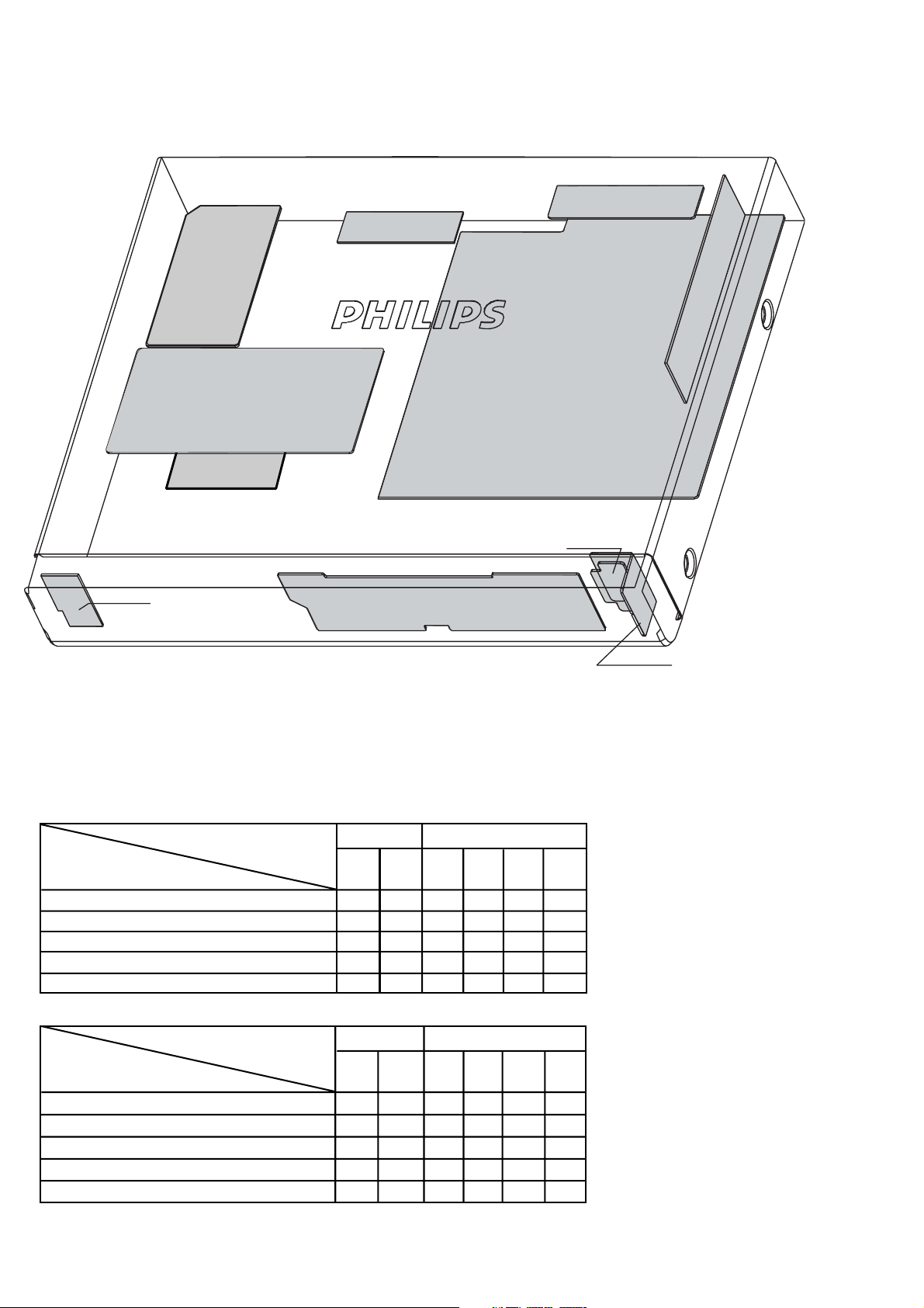
LOCATION OF PC BOARDS
1-2
RGB PCB
SPEAKER JACK PCB
LED PCB
POWER PCB
MPEG PCB
SERVO PCB
TUNER PCB
MAIN PCB
VOLUME PCB
KEY PCB
EAR PHONE PCB
VERSION VARIATION:
Type /Versions: MRD200 LX2000D
Features &
Board in used
RDS function
Progressive scan
RGB board x x x x x x
Power PCB (120V) x x
Power PCB (220-240V) x x x x
SW200 / 17 x
SW200 / 17S x
SW2000 / 00S x x
SW2000 / 02S x
SW2000 / 15S x
/37 /37S /21H /30S /33S /35S
Type /Versions: MRD200 LX2000D
/37 /37S /21H /30S /33S /35S

1-3
SPECIFICATIONS
AMPLIFIER SECTION
Power Output
- Stereo mode (DIN)................................................2 x 20 W
- Surround mode (1 kHz)............................20 W RMS/channel
Total Harmonic Distortion...........10 % at rated power (1 kHz)
Frequency Response .........................180 Hz-14 kHz/±1 dB
Signal-to-Noise Ratio........................................> 65dB(CCIR)
Input Sensitivity...........................................................400 mV
TUNER SECTION
Tuning Range ( /37,/37S )
.................................... FM 87.5 -108 MHz (100 kHz steps)
..........................................AM 530 - 1700 kHz (10 kHz steps)
Tuning Range ( /21H, /30S, /33S, /35S )
...................................... FM 87.5 -108 MHz (50 kHz steps)
..........................................MW531 - 1602kHz (9 kHz steps)
26 dB Quieting Sensitivity......................................FM 20 dB
26 dB Quieting Sensitivity..............................AM 3162 uV/m
Image Rejection Ratio...........................................FM 25 dB
................................................................................AM 28 dB
IF Rejection Ratio..................................................FM 60 dB
................................................................................AM 24 dB
Signal-to-Noise Ratio..............................................FM 60 dB
................................................................................AM 40 dB
AM Suppression Ratio...........................................FM 30 dB
Harmonic Distortion.........................................FM Mono 3%
..........................................................................FM Stereo 3%
.....................................................................................AM 5%
Frequency Response.....................FM 180 Hz-10kHz/±6 dB
Stereo Separation.........................................FM 26 dB(1 kHz)
Stereo threshold..................................................FM 23.5 dB
DVD SECTION
Audio Performance :
Laser Type......................................................Semiconductor
Disc Diameter.........................................................12cm/8cm
Video S/N ratio...............................................65 dB/A - WTD
Audio DAC........................................................24 Bits/96 kHz
Frequency Response...........................4 Hz-20 kHz (44.1kHz)
............................................................. 4 Hz-22 kHz (48 kHz)
............................................................. 4 Hz-44 kHz (96 kHz)
Digital Output....................................SPDIF Coaxial & Optical
Distortion.........................................................0.5% (1kHz)
MP3 :
MP3 - CD bit rate......................32, 64, 96, 128, 192, 256(kbps)
MP3 - CD sampling frequencies..............32, 44.1, 48(KHz)
Recording format.......................................................JPEG
Video Performances :
Video Decoding......................................................MPEG-2
Video DAC....................................................................10 Bits
Signal System........................................................PAL/NTSC
Video Format..........................................................4:3/16:9
Composite Video Output.....................................1.0Vp-p,75
S-Video Output.............................................Y - 1.0Vp-p,75Ω
..................................................................C - 0.286Vp-p,75Ω
MISCELLANEOUS / GENERAL SECTION
Power Supply Rating (/37,/37S)........................120V/60 Hz
Power Supply Rating (/21H,/30S,/33S,/35S)..220-240V/50Hz
Power Consumption.................................................. 120 W
Dimensions (w x h x d)............... 435 mm x 78 mm x 360mm
Weight...........................................................................7.1 kg
IR REMOTE CONTROL
Effective Range.........................................................> 8 Meter
Number of Keys................................................................45
Battery (1.5V)............................................................AA x 2
SPEAKERS
Front Speakers / Rear (Surround) speaker
System............................................................2-way shielded
Impedance/ ohm................................................................8Ω
Speaker drivers.....................................................3" full range
Dimensions (w x h x d)................... 94 mm x 155 mm x 88 mm
Weight.............................................................. 0.45 Kg/each
Center Speaker
System............................................................2-way shielded
Impedance/ ohm................................................................8Ω
Speaker drivers.........................................2 x 3" woofer, piezo
Dimensions (w x h x d)...................250mm x 95 mm x 88 mm
Weight............................................................... 0.92 Kg/each
Ω

1-4
AC MILLIVOL TME TER
SIGNAL GENERATORAC
OUTPUT
AUTO DISTORTION METER
AM-FM STEREO SIGNAL
GENERATOR
INPUT OUTPUT
AM SECTION
OSCIL LOSCOPE
............
............
LOOP
AM LOOP ANT
LOAD 4 OHM
INPUT
RL
DUT
AC MILLIVOL TME TER
SIGNAL GENERATORAC
OUTPUT
AUTO DISTORTION METER
AM-FM STEREO SIGNAL
GENERATOR
INPUT OUTPUT
OSCIL LOSCOPE
............
............
FM SECTION
LOAD 4 OHM
INPUT
RL
DUT
AC MILLIVOL TME TER
SIGNAL GENERATORAC
OUTPUT
AUTO DISTORTION METER
DOLBY TEST METER
INPUT OUTPUT
AUX SECTION
OSCIL LOSCOPE
............
............
LOAD 4 OHM
.......
............
DUT
INPUT
.......
............
............
.......
............
.......
AC MILLIVOL TME TER
AUTO DISTORTION METER
DVD TEST DISC
DISC SECTION
OSCIL LOSCOPE
............
............
DUT
LOAD 4 OHM
.......
............
R L C SRSLSWR L C SRSLSW
INPUT
.......
............
............
.......
............
.......

SERVICE AIDS
1-5
Service Tools:
Universal Torx driver holder .................................4822 395 91019
Torx bit T10 150mm ...........................................4822 395 50456
Torx driver set T6-T20 .........................................4822 395 50145
Torx driver T10 extended .....................................4822 395 50423
Compact Disc:
SBC426/426A Test disc 5 + 5A ...........................4822 397 30096
SBC442 Audio Burn-in test disc 1kHz .................4822 397 30155
SBC429 Audio Signals disc .................................4822 397 30184
Dolby Pro-logic Test Disc ....................................4822 395 10216
HANDLING CHIP COMPONENTS
ESD Equipment:
Anti-static table mat - large 1200x650x1.25mm ...4822 466 10953
anti-static table mat - small 600x650x1.25mm .....4822 466 10958
Anti-static wristband ............................................4822 395 10223
Connectorbox (1MΩ) ..........................................4822 395 11307
Extension cable
(to connect wristband to conn.box) ..........4822 320 11305
Connecting cable
(to connect table mat to conn.box) ...........4822 320 11306
Earth cable (to Connect product to mat or box) --4822 320 11308
Complete kit ESD3
(combining all above products) ...............4822 320 10671
Wristband tester ...................................................4822 344 13999
WARNING
GB
All ICs and many other semi-conductors are
susceptible to electrostatic discharges (ESD).
Careless handling during repair can reduce life
drastically.
When repairing, make sure that you are
connected with the same potential as the mass
of the set via a wrist wrap with resistance.
Keep components and tools also at this
potential.
F
ATTENTION
Tous les IC et beaucoup d’autres
semi-conducteurs sont sensibles aux
décharges statiques (ESD).
Leur longévité pourrait être considérablement
écourtée par le fait qu’aucune précaution n’est
prise à leur manipulation.
Lors de réparations, s’assurer de bien être relié
au même potentiel que la masse de l’appareil et
enfiler le bracelet serti d’une résistance de
sécurité.
Veiller à ce que les composants ainsi que les
outils que l’on utilise soient également à ce
potentiel.
1-6
ESD
D
WARNUNG
Alle ICs und viele andere Halbleiter sind
empfindlich gegenüber elektrostatischen
Entladungen (ESD).
Unsorgfältige Behandlung im Reparaturfall kan
die Lebensdauer drastisch reduzieren.
Veranlassen Sie, dass Sie im Reparaturfall über
ein Pulsarmband mit Widerstand verbunden
sind mit dem gleichen Potential wie die Masse
des Gerätes.
Bauteile und Hilfsmittel auch auf dieses gleiche
Potential halten.
WAARSCHUWING
NL
Alle IC’s en vele andere halfgeleiders zijn
gevoelig voor electrostatische ontladingen
(ESD).
Onzorgvuldig behandelen tijdens reparatie kan
de levensduur drastisch doen verminderen.
Zorg ervoor dat u tijdens reparatie via een
polsband met weerstand verbonden bent met
hetzelfde potentiaal als de massa van het
apparaat.
Houd componenten en hulpmiddelen ook op
ditzelfde potentiaal.
I
AVVERTIMENTO
Tutti IC e parecchi semi-conduttori sono
sensibili alle scariche statiche (ESD).
La loro longevità potrebbe essere fortemente
ridatta in caso di non osservazione della più
grande cauzione alla loro manipolazione.
Durante le riparazioni occorre quindi essere
collegato allo stesso potenziale che quello della
massa dell’apparecchio tramite un braccialetto
a resistenza.
Assicurarsi che i componenti e anche gli utensili
con quali si lavora siano anche a questo
potenziale.
GB
Safety regulations require that the set be restored to its original
condition and that parts which are identical with those specified,
be used.
NL
Veiligheidsbepalingen vereisen, dat het apparaat bij reparatie in
zijn oorspronkelijke toestand wordt teruggebracht en dat onderdelen,
identiek aan de gespecificeerde, worden toegepast.
F
Les normes de sécurité exigent que l’appareil soit remis à l’état
d’origine et que soient utiliséés les piéces de rechange identiques
à celles spécifiées.
D
Bei jeder Reparatur sind die geltenden Sicherheitsvorschriften zu
beachten. Der Original zustand des Geräts darf nicht verändert werden;
für Reparaturen sind Original-Ersatzteile zu verwenden.
“Pour votre sécurité, ces documents
doivent être utilisés par des spécialistes agréés, seuls habilités à réparer
votre appareil en panne”.
CLASS 1
LASER PRODUCT
GB
Invisible laser radiation when open.
Avoid direct exposure to beam.
Osynlig laserstrålning när apparaten är öppnad och spärren
är urkopplad. Betrakta ej strålen.
Warning !
S
Varning !
3122 110 03420
I
Le norme di sicurezza esigono che l’apparecchio venga rimesso
nelle condizioni originali e che siano utilizzati i pezzi di ricambio
identici a quelli specificati.
"After servicing and before returning set to customer perform a
leakage current measurement test from all exposed metal parts to
earth ground to assure no shock hazard exist. The leakage current
must not exceed 0.5mA."
Varoitus !
SF
Avatussa laitteessa ja suojalukituksen ohitettaessa olet alttiina
näkymättömälle laserisäteilylle. Älä katso säteeseen!
DK Advarse !
Usynlig laserstråling ved åbning når sikkerhedsafbrydere er
ude af funktion. Undgå udsaettelse for stråling.
2-1
2-1
System, Region code, Tuner, etc. setting procedure
1) System Reset
a) Press "SYSTEM" button on R/C. TV show "SETUP"
b) Select the menu using the " " and " " button on R/C
c) Go feature setup page to do system reset
2) Region Code Change
After replacement / repair of the MPEG board, the customer
setting and the reegion code may lost. Changing the Region
Code will put the player back in the state which it has left the
factory.
Region Code
1 USA
2EU
3AP
4 Australia, NZ, Latam
5 RUSSIA, INDIA
6 CHINA
TV System
1 NTSC
2PAL
3AUTO
Menu/ Audio Subtitle (AS) Language
1 English
2 English
3 English
4 English
Hence in total, reprograming will be done by way of the
remote control. It should run as below :-
a) Put the player in stop mode. No disc loaded.
b) Press the following key on remote control:
For MRD200/37/37S (USA) :
<PLAY> <159> <111> <001> <08> <PLAY>
For LX2000D/21H (AP) :
<PLAY> <159> <331> <001> <08> <PLAY>
For LX2000D/30S (NZ, Australia) :
<PLAY> <159> <431> <001> <08> <PLAY>
For LX2000D/33S (Korea) :
<PLAY> <159> <311> <001> <08> <PLAY>
For LX2000D/35S (China) :
<PLAY> <159> <631> <001> <08> <PLAY>
∗ After the Region Code is changed it is necessary to reset
the system so that the new Region Code will be fully
effective. All customer setting will be lost.
∗ On top of the maximum number of times allowed for
changing the region code is changed to 25.
∗ When the counter reeach 25, you will not be able to further
AFS
001 LX2000D/LX3000D/LX3500D/ MRD200
002 MX3550D/MX3600D/MX3700D/MX3800D
change the code until you reset the timer by the Region
Code timer reset procedure.
3) Region code change timer reset
Press below key to reset the timer :
a) In DISC source, stop mode and no disc in tray.
b) Press R/C "Play -159-PLAY" to reset timer to 25
4) Tuner area change
a) Press the "OPEN/CLOSE" button to openthe set's door
b) Press "1" "5" "9" button by using R/C.
c) TV Show "TUNER AREA ADJUST"
d) Select the tuner area you want by using the "
" button on R/C, then press "OK" to confirm. TV show
"
" TUNER AREA CHANGED"
If you didn't press it in five seconds, the system will remain
original status.
AREA BAND FREQUENCY (Hz) STEP(Hz)
USA FM 87.5M 108M 100K
AM 530K 1700K 10K
APAC FM 87.5M 108M 50K
AM 531K 1602K 9K
EUROPE FM 87.5M 108M 50K
AM 531K 1602K 9K
LATAM FM 87.5M 108M 50K
AM 530K 1710K 10K
AUSTRALIA FM 87.5M 108M 50K
/ NZ AM 531K 1602K 9K
Note :-
Please refer to the above different tuner area.
" and
5. Video Out Change
a) Press "SYSTEM" on R/C button
b) Select the menu using the " " and " " button on R/C
c) Go picture setup page select Video out item.
6. Password Change
a) Press "SYSTEM" on R/C button.
b) Select the menu using the "
c) Go feature setup page select "PASSWORD". TV show
"ENTER CODE". Press 4 times of "STOP" button on R/C.
d) Select "PARENTAL" "8 ADULT" on TV.
e) Enter PASSWORD to "1234".
" and " " button on R/C.
∗ "1234" is a default password supplied.
7. Checking on the Software version
a) Open the CD door.
b) Press "123" and "OK" on the remote control.
c) TV will show the version on screen.
8. Upgrading new software
a) Open the CD-door, then insert the CD-R program disc.
b) Close the CD-door.
c) TV will show:-
.
"disc loading"
.
"bank30.rom"
.
"writing" about 6 seconds.
.
"Done"
∗
The latest upgraded is in version VER0527.
oem derivative
08
.
region code = 1 digit
.
tv system = 1 digit
.
"as/menu lang" = 1 digit
.
"AFS" = "architechture Feature Set" = 3 digits
This field is used to define the architecture / features sets for
each product.
.
"oem derivative" = 2 digit
This field is use to define the OEM set. This will affect the
background display.
CAUTION !
This information is confidencial and may not
be distributed. Only a qualified service
person should reprogram the Region Code.

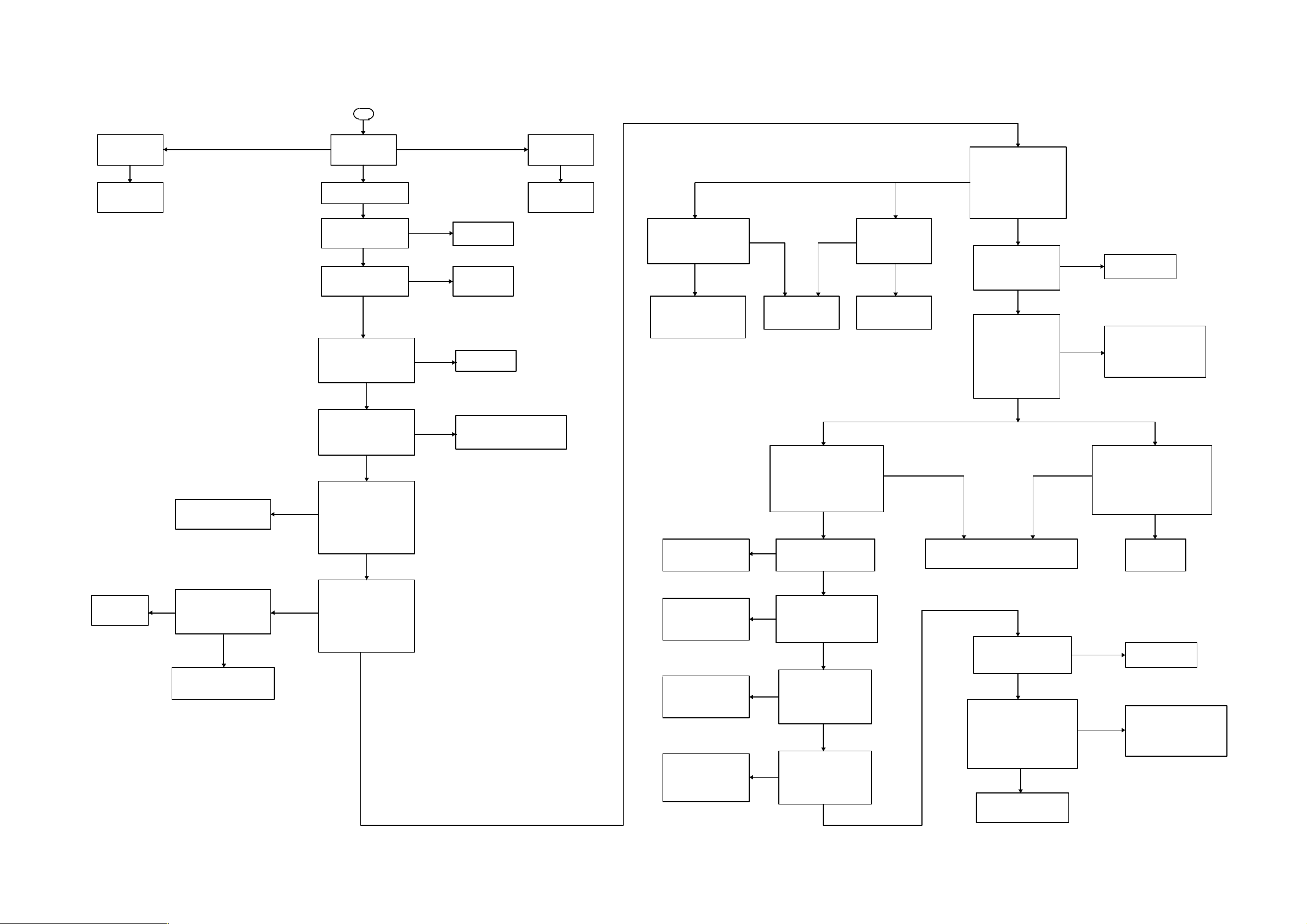
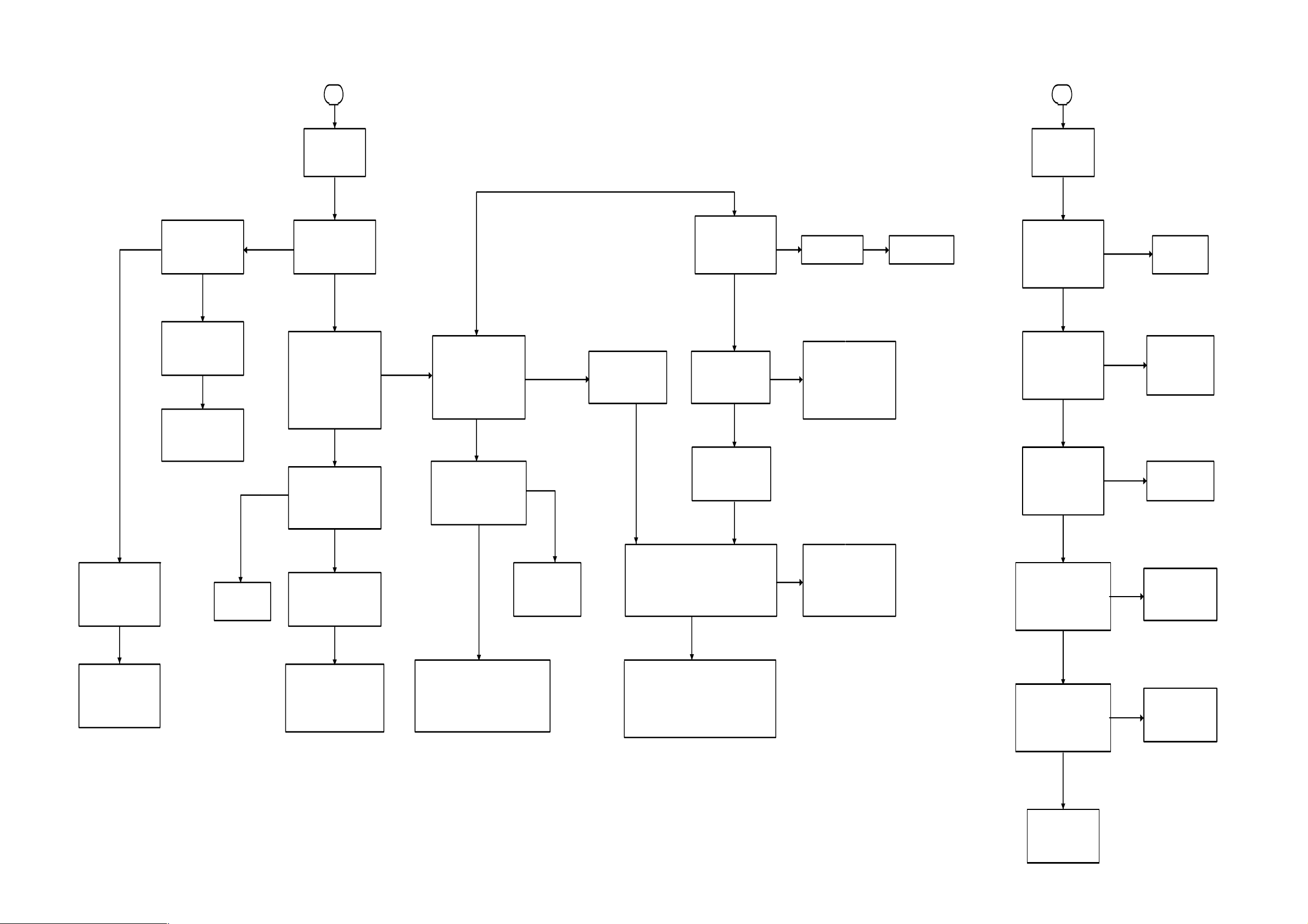
REPAIR INSTRUCTIONS
2-2
2-2
MAIN UNIT REPAIR CHART
Change F981
Check Back power BD
Bad
F981
Bad Cause Damage
Check CN203
Pin3=(+5V)
Between T981 to IC982
Repair
Circuit
All Function
No Working
Not
OK
No
A
B
VFD Display
No Show
And Key Function
Yes
Check Repair
Control BD IC981
circuit
C
Audio Output
No Sound
Check All System
All cable is loose
Panel stanby LED show
Working or Not
Check Main BD fuse F903
Bad Cause Damage
No
Check back power BD
Systm power control
CN203 Pin1 =(+ 5V)
Check main BD
IC903 Pin3 to
RB900 Pin1,3 = 5V
Check Mpeg BD section
All power supply
All VCC=(+5V)
All VCC33=(+3.3V)
DVD Audio
No Output
A
All function
No Working
or bad INT
No
Work
OK
Yes
Yes
D
E
Aux/TV
No Output
F
Tuner
No Output
G
Ear Head Phone
No Sound
H
Audio Line
No Output
I
Center Line
No Output
J
Subwoofer Line
No Output
K
Digital Line
No Output
B
VFD Display
No Show
And Key Function
Yes
Bad
No
No
RE-Insert and fix
the cable
Change F903
Change T901
Check T901
Bad Cause Damage
Change IC903
Repair Mpeg BD section
All power supply circuit
Bad
Ok
Check +5V
Power Supply Circuit
Check T901 CN904
And Fuse Resistor
R925. R926. R927
Power Supply Circuit
Pin7 No +5V
No
Check Test CN201
Pin7=+5V
Pin8=-26V
Pin9.11=AC1.2V
Pin10=AC0V
Check VFD Control BD Section Bad Cause Damage
Check Control BD CN205
And Standby BD RB202
Cable loose or bad INT
No
Check Control BD CN205 Pin6
And Standby BD RB202 Pin3
Yes Or No (+5V)
Yes
Check Main BD CN201
And CN904
Cable loose or bad INT
No
Check Test CN201 Data From
Mpeg BD CPU To RB102 Cable
Yes Yes
Yes
No
Yes
Pin4/CE
Pin5/CLOCK
Pin6/DATA
RE-Insert and fix
the cable
Check Back Power Bd
Power Supply Circuit
RE-Insert and fix
the cable
No Data
Check RB102
Cable loose or bad INT
No
Check Mpeg BD IC6(CPU)
And IC2 Bad Cause Damage
Yes
RE-Insert and fix
the cable
Yes
Check Mpeg BD
IC6(CPU) Pin24(Reset) and
Pin49(OSC frequency 27MHz)
Yes
Repair Mpeg BD
Between IC6(CPU) to
IC1,IC7,IC9 circuit
Note: BD=Board
Main BD = LVM0189C011
MPEG BD = LFF0205C001
Surround BD = LVA0192C001
Tuner BD = LVT0187C001
Check IC405,IC406
At DVD AC3 Dolbly Digital Mode
IC405 Pin13=D/L
Pin1=D/R
Audio Signal input
Pin3=D/C
Pin2=L/CH
Check surround BD CN601
Pin3=R/CH
Audio signal output
Pin13 to C412 = L/Ch
Pin3 to C416 = R/CH
Audio Signal input
Between Ic405.406 Pin9.10.11
Yes
No
Pin3=+Vcc(+17.5V to +20V)
IC501 Pin7 from C473(L-CH)
IC501 Pin11 from C478(R-CH)
IC502 Pin11 from C491(C-CH)
IC503 Pin7 from C483(SL-CH)
IC503 Pin11 from C487(SR-CH)
Audio signal output
Pin31 to C471(L-CH)
Pin32 to C476(R-CH)
Pin33 to C489(C-CH)
Pin34 to C481(SL-CH)
Pin35 to C485(SR-CH)
Pin4=(-12V)
Pin8=(+12V)
Pin15 from C437(L-CH)
Pin13 from C438(R-CH)
Pin11 from C439(C-CH)
Pin9 from C440(SL-CH)
Pin8 from C441(SR-CH)
Repair
From C495 to subwoofer output
Pin36 to C493(Subwoofer)
Pin6 from C442(Subwoofer)
Pin30=(-7V)
Pin5=(+7V)
(Surround mode)
Ic405 Ic406 Pin9.10.11 = (0V)
1: At aux/TV, tuner mode
(5.1 CH mode)
1: At DVD dolby mode
IC406 Pin13=D/SR
Pin1=D/SL
Pin3=D/subwoofer
IC405 Pin12=P/L
Pin2=P/R
Pin5=P/C
IC406 Pin2=P/SR
Pin12=P/SL
Pin5=P/subwoofer
Yes
Yes
RB601 Audio Signal output
Pin4=R
Pin5=L
Pin6=C
Pin7=SR
Pin10=SL
Control voltage Pin9=(0v)
Audio Signal input
Pin16(VDD)=+7V
Pin7(VEE)=-7V
Switch control voltage
Pin10=(A)
Pin9=(B)
(Pin10=+5V, Pin9=0V) for aux mode
(Pin10=0V, Pin9=0V) for TV mode
(Pin10=0V, Pin9=+5V) for DVD line out
REPAIR INSTRUCTIONS
2-3
2-3
C
Aux/TV/Tuner
No output
See (E) and (F)
Repair chart
Change
R4105 or R4106
Change Amplifier IC
IC501 or IC502 or IC503
Check IC409 IC410 IC411
No
Check IC409 IC410 IC411
Bad Cause Damage
Power supply
Pin4=(-12V)
Pin8=(+12V)
Yes
Yes
Yes
Audio output
No Sound
All channel no oosund
Check all cable is loose
or bad INT
No
Check fuse F901/F902
Bad Cause Damage
OK
Check Amplifier
IC501/IC502/IC503
Power supply
Pin1=-Vss(-17.5V to -20V)
Pin3=+Vcc(+17.5V to +20V)
Yes
Check system power supply
IC901 Pin3=(-12V)
IC902 Pin3=(+12V)
Yes
Check IC501/IC502/IC503
Audio signal input
IC501 Pin7 from C473(L-CH)
IC501 Pin11 from C478(R-CH)
IC502 Pin11 from C491(C-CH)
IC503 Pin7 from C483(SL-CH)
IC503 Pin11 from C487(SR-CH)
From C495 to subwoofer output
No
Check IC408
Audio signal output
Pin31 to C471(L-CH)
Pin32 to C476(R-CH)
Pin33 to C489(C-CH)
Pin34 to C481(SL-CH)
Pin35 to C485(SR-CH)
Pin36 to C493(Subwoofer)
No
Yes
Bad
No
No
DVD audio
No output
See (D)
Repair chart
RE-Insert and fix
the cable
Change fuse
F901 orF902
Change D901
Check IC901,IC902 or R901,R902
Bad Cause Damage
Check IC408 data
Pin39 from RB102 Pin26(CE)
Pin40 from RB102 Pin14(data)
Pin41 from RB102 Pin24(clk)
No
Check Mpeg BD section
Between IC6(CPU) to IC2,IC3
to CN102 circuit
Repair power Supply circuit
Repair
Between CN601 to
IC405,IC406 circuit
Repair
Surround BD circuit
Repair
Between IC402 to CN601
Pin2 and Pin3 circuit
And power supply circuit
Ok Ok
Change IC408
At aux/TV, tuner mode
(Surround mode)
Check Ic405 Ic406
Audio Signal input
IC405 Pin12=P/L
IC406 Pin2=P/SR
Check Surround BD
No
Pin13=(+12V) Pin14=(-12V)
Check Surround BD6CH mode
Yes
Control voltage Pin9=(0v)
RB601 Audio Signal output
Pin4=R
Pin7=SR
Pin2=P/R
Pin12=P/SL
Pin5=P/subwoofer
No
Power Suply:
Yes
Pin5=L
Pin10=SL
No
Check surround BD CN601
Yes
Audio Signal input
Pin2=L/CH
Pin3=R/CH
No
Yes
At aux/TV, tuner mode
Check Ic401
Audio signal output
Pin13 to C412 = L/Ch
Pin3 to C416 = R/CH
Pin5=P/C
CN601
Pin6=C
Yes
Check IC408
Power supply
Pin30=(-7V)
Pin5=(+7V)
No
Change
R466 or R467
Yes
Check volume control IC408
Audio signal input
Pin15 from C437(L-CH)
Pin13 from C438(R-CH)
Pin11 from C439(C-CH)
Pin9 from C440(SL-CH)
Pin8 from C441(SR-CH)
Pin6 from C442(Subwoofer)
No
Check IC405. IC406
Power Supply
Pin16(VCC)=+7V
PIN7(VEE)=-7v
Yes
Check IC405 IC406
Switch control voltage
1: At aux/TV, tuner mode
(Surround mode)
Ic405 Ic406 Pin9.10.11 = (0V)
1: At DVD dolby mode
(5.1 CH mode)
Ic405 Ic406 Pin9.10.11 = (+5V)
Change IC405 , IC406
No
Check IC401 power supply
Pin16(VDD)=+7V
Pin7(VEE)=-7V
Yes
Check IC401Pin9 and Pin10
Switch control voltage
Pin10=(A)
(Pin10=0V, Pin9=0V) for TV mode
(Pin10=+5V, Pin9=0V) for aux mode
(Pin10=+5V, Pin9=+5V) for tuner mode
(Pin10=0V, Pin9=+5V) for DVD line out
Pin9=(B)
Yes
Change Ic401
No
No
Repair IC405,IC406
Power supply Circuit
Between Ic405.406 Pin9.10.11
To Ic408 Pin2 Circuit or
At DVD AC3 Dolbly Digital Mode
Yes
Check IC405,IC406
Audio Signal input
IC405 Pin13=D/L
IC406 Pin13=D/SR
Pin3=D/subwoofer
No
Power Supply circuit
No
Repair
IC408 Circuit
Pin1=D/R
Pin3=D/C
Pin1=D/SL
No
See (D)
Repair chart
Repair
Repair
Between IC401 Pin9,10 to
IC408 Pin3,4 Circuit or
IC408 Circuit

No Output
REPAIR INSTRUCTIONS
2-4 2-4
Check RB104 To Mpeg BD
Check RB104 6 Channels
Pin2=L Pin3=R
Pin6=SRPin8=C
D
DVD Audio
No Output
CN104
Cable loose or bad INT
No
Audio Signal
Pin5=SL
Pin9=Woofer
Yes
RE-Insert and fix
the cable
No Check Mpeg Bd
D/A section
E
Aux/TV
No Output
Check Main BD
Between JK401 to IC401
Circuit
Ok
See(C)
Repair chart (at surround mode)
Of IC401 section circuit
Repair
Bad
Between JK401 to IC401
Circuit
Yes
Check
Between RB104 to IC405,IC406
circuit
Ok
See(C)
Repair chart (at DVD mode)
Of IC405,IC406 section circuit
Bad
Repair
Between RB104 to IC405,IC406
circuit
Power supply
From C161
IC101 Pin16 to RB101 Pin13 (R-CH)
Yes
REpair FM IF section:
Q910 or Q911 or Q912
From RB101
Pin14/FM input
Check Main BD RB102
Cable loose or bad INT
Check Q103/Q104
Between Main BD CN101
to RB102 Circuit
Check Mpeg BD CPU IC6
And IC2/IC3 Bad Cause Damage
Pin6=12V
Check IC152 or
Yes
Check FM IF output
Check T105
OK
IC101 Pin17 to RB101 Pin15 (L-CH)
REpair FM IF section:
Between EF001 to Q101/Q102
CN101 Pin13 to IC401 Pin4 (R-CH)
CN101 Pin15 to IC401 Pin11 (L-CH)
(From Main BD)
Cable loose or bad INT
the cable
Ear head phone BD RB301
No
Repair Power Supply
To main BD CN301
Pin6=(+12V)
Ear head phone BD RB301
To main BD CN301
No
Repair Power Supply
(Q308) Circuit
Ear head phone BD
No
Pin7 from RB301 Pin5=(R/CH)
Audio signal input
Between R472, R478
(From main BD)
No
Pin3 to FB301=(L/CH)
Audio signal output
Pin1 to FB302=(R/CH)
Change phone jack
REPAIR INSTRUCTIONS
2-5 2-5
Check RB101
Pin12=5V
Pin11=12V
Check Q910/Q911/Q912
From Main BD
Change
Q910 or Q911 or Q912
No
Yes
No
Yes
F
Tuner No Output
Check to tuner
Power supply
Yes
Check IC152 Data
From RB101
Pin3/CE
Pin4/DI
Pin5/CL
Pin6/DO
No
Check Main BD RB102
Cable loose or bad INT
Yes
Yes
Check tuner VT
From C161
Low frequency=1.5-2.0V
Yes
No AM function
Higt frequency=8.0-9.0V
VT No Change
Check IC152 osc input
Pin13/AM input
Pin14/FM input
No FM function
Check tuner pack EF001
Check FM IF output
Check AM IF T102/CF103
Power supply
Pin6=12V
No Yes
Yes
No
Q101/Q102
Yes
Check T105
Check Q103/Q104
Cnange Q103/Q104
REpair FM IF section:
Between EF001 to Q101/Q102
to IC101 Pin1 circuit
G
EAR Head Phone
No Sound
Check
Ear head phone BD RB301
Yes
To main BD CN301
Cable loose or bad INT
No
Check
Ear head phone BD RB301
No
To main BD CN301
Pin6=(+12V)
Yes
Check
Ear head phone BD
No
IC304
Pin2=(+6V)
RE-Insert and fix
Repair Power Supply
Repair Power Supply
the cable
Circuit
(From main BD)
(Q308) Circuit
YES
Check
IC152 Pin15=5V
IC101 Pin8=12V
No
Change
L153 or L154/L104
No
Check
RE-Insert and fix
the cable
Between Main BD CN101
to RB102 Circuit
No
Check Mpeg BD CPU IC6
And IC2/IC3 Bad Cause Damage
A: Repair Am osc section (T003) or
(Between IC101 Pin30 to IC152 Pin13 circuit)
B: Repair Fm osc section
(Between EF001 Pin8 to IC152 Pin14 circuit)
No
Yes
Check IC152 or
VT section
Circuit
OK
Check IC101 audio output
IC101 Pin16 to RB101 Pin13 (R-CH)
IC101 Pin17 to RB101 Pin15 (L-CH)
Repair tuner signal input circuit
CN101 Pin13 to IC401 Pin4 (R-CH)
CN101 Pin15 to IC401 Pin11 (L-CH)
OK
Yes
(From Main BD)
REpair FM IF section:
No
Between EF001 to Q101/Q102
to IC101 Pin1 circuit
Yes
Check IC304
Audio signal input
Pin6 from RB301 Pin4=(L/CH)
Pin7 from RB301 Pin5=(R/CH)
Yes
Check IC304
Audio signal output
Pin3 to FB301=(L/CH)
Pin1 to FB302=(R/CH)
Yes
Change phone jack
Repair main BD
No
Between R472, R478
to CN301 circuit
No
Change IC304
JK301
Check main BD
Pin4=(-12V)
Repair IC407
Power supply circuit
No
IC407 power supply
Check IC407
Pin7 to C449=(L/CH)
Audio Signal output
Pin1 to C454=(R/CH)
Yes
Repair
Yes
Check IC407
No
Of IC401 to IC402 section circuit
See(C)
Yes
Chage IC407
Repair chart
Audio Line
No Output
Check IC413
Pin3 from C4008
Audio Signal input
No
Yes
(Center line out)
Repair
Between C4004 to JK402 Circuit
Center Line
No Output
Check main BD
Subwoofer Signal output
C495 to R409 to JK402
No
Yes
Between IC411 to IC405,IC406
See (C) Repair chart
circuit
Subwoofer Line
No Output
At DVD mode
JK106 Pin2 power supply
No
Check main BD
Yes
Digital Line
No Output
Pin8=(+12V)
No
circuit
Audio Signal input
At DVD mode
No DVD line out
All function
IC407 power supply
At (surround) mode
No Aux/TV/tuner line out
Repair
between (RB104 Pin1,Pin2)
to (IC401 Pin2,Pin15) circuit
No
No
See (E) and (F)
Repair chart
Check main BD
Pin4=(-12V)
Repair IC413
Power supply circuit
No
IC413 power supply
Pin8=(+12V)
Between C4008 to R490 Circuit
Repair
Check IC413
Pin1 to C4004
Audio Signal output
No
Yes
Change IC413
Yes
Yes
(Woofer out)
Repair
Circuit
Between C495 to JK402
(At DVD mode) and (Surround)
Check at surround mode
Subwoofer signal output
IC404 Pin7 to C435
Check at DVD mode
Subwoofer signal input
IC406 Pin3
No
See (D)
Repair chart
No
Check main BD
Pin4=(-12V)
Repair
Power supply circuit
No
IC403 and IC404
Pin8=(+12V)
Power supply
IC403 and IC404
No
Check IC403
Subwoofer signal input
Pin2 from C420,C421
Repair
circuit
Between IC403 to IC404
Yes
See(C)
IC401 to IC406 circuit
Repair chart
No
Repair JK106
Power supply circuit
Check
JK106 Pin1 digital signal
Change JK106
Yes
Check
RB102 Pin15 digital signal
No
Check
Between JK106 Pin1 to RB102 Pin15
circuit
Yes
Check MPEG BD
Betweeen CN102 Pin15 to IC6 Pin41
circuit
No
REPAIR INSTRUCTIONS
2-6 2-6
H
Audio Line
No Output
All function
IC407 power supply
Check main BD
IC407 power supply
Pin8=(+12V)
Pin4=(-12V)
Yes
Check IC407
Audio Signal output
Pin7 to C449=(L/CH)
Pin1 to C454=(R/CH)
No
Check IC407
Audio Signal input
Pin5 from C447 to R422=(L/CH)
Pin3 from C452 to R428=(R/CH)
Yes
Chage IC407
At (surround) mode
No Aux/TV/tuner line out
No
See (E) and (F)
Repair chart
No
Yes
No
Repair chart
Of IC401 to IC402 section circuit
Repair IC407
Power supply circuit
Repair
Between C449 ,C454 to JK401(audio out)
circuit
See(C)
At DVD mode
No DVD line out
No
Repair
between (RB104 Pin1,Pin2)
to (IC401 Pin2,Pin15) circuit
Pin4=(-12V)
Between C4004 to JK402 Circuit
I
Center Line
No Output
Check main BD
IC413 power supply
Pin8=(+12V)
Yes
Check IC413
Audio Signal input
Pin3 from C4008
Check IC413
Audio Signal output
Pin1 to C4004
(Center line out)
Yes
Yes
Repair
No
No
No
Repair IC413
Power supply circuit
Repair
Between C4008 to R490 Circuit
Change IC413
Check at surround mode
Subwoofer signal output
IC404 Pin7 to C435
Pin4=(-12V)
Subwoofer signal input
Pin2 from C420,C421
IC401 to IC406 circuit
J
Subwoofer Line
No Output
Check main BD
(At DVD mode) and (Surround)
Subwoofer Signal output
C495 to R409 to JK402
(Woofer out)
No
See (C) Repair chart
Between IC411 to IC405,IC406
circuit
No
Check main BD
IC403 and IC404
Power supply
Pin8=(+12V)
Yes
Check IC403
No
See(C)
Repair chart
Yes
No
Yes
Repair
Between C495 to JK402
Circuit
No
Check at DVD mode
Subwoofer signal input
IC406 Pin3
No
See (D)
Repair chart
Repair
IC403 and IC404
Power supply circuit
Repair
Between IC403 to IC404
circuit
JK106 Pin2 power supply
JK106 Pin1 digital signal
RB102 Pin15 digital signal
Betweeen CN102 Pin15 to IC6 Pin41
K
Digital Line
No Output
At DVD mode
Check main BD
Yes
Check
Check MPEG BD
No
Check
No
circuit
No
Yes
Yes
Repair JK106
Power supply circuit
Change JK106
Check
Between JK106 Pin1 to RB102 Pin15
circuit
REPAIR INSTRUCTIONS
DVD SECTION REPAIR CHART
2-7 2-7
L
Tray cannot
open
Tray cannot open
Check loader server BD
CN600 to moter CN001
Cable loose or bad INT
Check loader server BD
CN900 to moter RB900
Cable loose or bad INT
Check main BD RB900
Pin1,3=(+5V)
Pin5=(+9V)
Check Repair
Loader server BD
IC602 circuit
Cannot read
Disc or
Intermittent
L
No
No
Yes
M
Yes
Yes
No
RE-Insert and fix
the cable
RE-Insert and fix
the cable
Repair main BD
Power supply circuit
Video output
No signal
Cannot read the disc
or intermittent
Check loader server BD
CN610 And CN100
Cable loose or bad INT
Check loader server BD
CN200 to MPEG BD CN1
Cable loose or bad INT
Check Repair
A: Loader LD head BD
B: Loader server BD
ON
No sound
Analog no output
M
No
No
Circuit
Circuit
Yes
Yes
RE-Insert and fix
the cable
RE-Insert and fix
the cable
RE-Insert and fix
the cable
Check Repair
IC6 MPEG decoder
Section circuit
CVBS-Video
no output
Yes
No
Check MPEG BD
CN107 to Video jack BD
Cable loose or bad INT
Check MPEG BD
IC6 Pin114 to CN107 Pin2
CVBS-video signal output
Check Repair
Check Video jack BD
Circuit
No
Yes
N
Video output
No signal
S-Video(UL)
SCART Video(CE)
no output
Check MPEG BD
CN108 to Video jack BD
Cable loose or bad INT
No
Check MPEG BD CN108
Video signal output
1. (UL) S-Video C/Y Pin5,6
2. (CE) R,G,B/Pin4,3,2
Yes
Check Repair
Check Video jack BD
Circuit
No
Yes
RE-Insert and fix
the cable
Check MPEG BD IC6
Video signal output
1. Pin106=UDAC
2. Pin108=CDAC
3. Pin113=YDAC
Yes
Check Repair IC6
Between Pin 106,108,113 to
CN108 Pin4,3,2 circuit
No
Check Repair
IC6 MPEG decoder
Section circuit
Video jack BD
(LVB0184C001) for
Model(LX3000D/MRD200D)
Video jack BD
(LVA0204C001) for
Model(LX3500D)
Note: BD=Board
MPEG BD = LFF0205C001
Video jack board(LX3000D/MRD200D)=LVB0184C001
Video jack board(LX3500D)=LVA0204C001
REPAIR INSTRUCTIONS
2-8 2-8
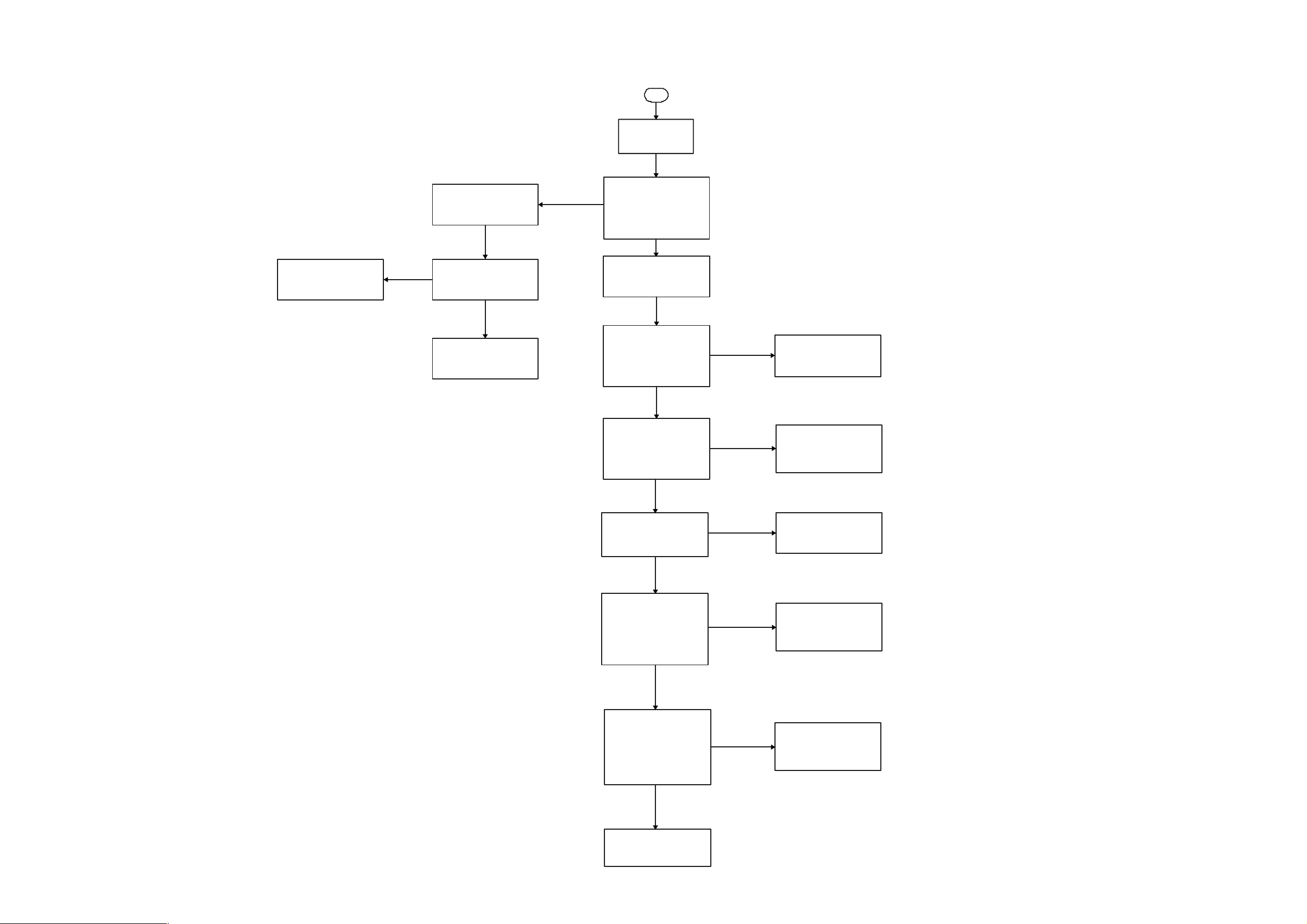
O
No Sound
Analog No Output
Repair IC18 power supply
Circuit
No
(b)
L, R, C /CH
No signal output
Check IC18 power supply
Pin16(VCC)=+7V
Pin7(VEE)=-7V
Yes
See (a)
Repair chart
Check MPEG BD CN104
Analog Signal output
Pin4=L/CH
Pin6=LS/CH
Pin9=C/CH Pin10=SUB/CH
Pin5=R/CH
Pin7=RS/CH
(a)
All Channal
No signal output
Check power supply
The follwing
IC11, IC12, IC13,
IC14, IC15, IC16, IC17
Pin8=(+12V) Pin4=(-12V)
Yes
Check analog Signal
C78=L/CH
C80=LS/CH
Pin82=C/CH C83=SUB/CH
C79=R/CH
C81=RS/CH
No
Yes
Repair power supply
Circuit
Check repair
Between C78, C79, C80, C81,
C82, C83, to CN108 Circuit
No
Check IC10
Power supply
Pin1,8,14,22=(+5V)
Yes
Check IC10 data
1. CCLK/Pin11 from IC2 Pin9
2. CDIN/Pin12 from IC2 Pin6
3. CS/Pin13 from IC2 Pin5
4. MCLK/Pin7 from IC6 Pin39
5. SCLK/Pin5 from IC6 Pin40
Yes
Check IC10 data
(Digital signal input)
1. LRCK/Pin6 from IC6 Pin32
2. SDIN1/Pin2 fronm IC6 Pin33
3. SDIN2/Pin3 from IC6 Pin36
5. SDIN3/Pin4 from IC6 Pin37
Yes
No
No
No
Repair power supply
Circuit
Check repair
Between IC2 to IC6 circuit
And IC6 Circuit
Check repair
IC6 Circuit
Change IC10
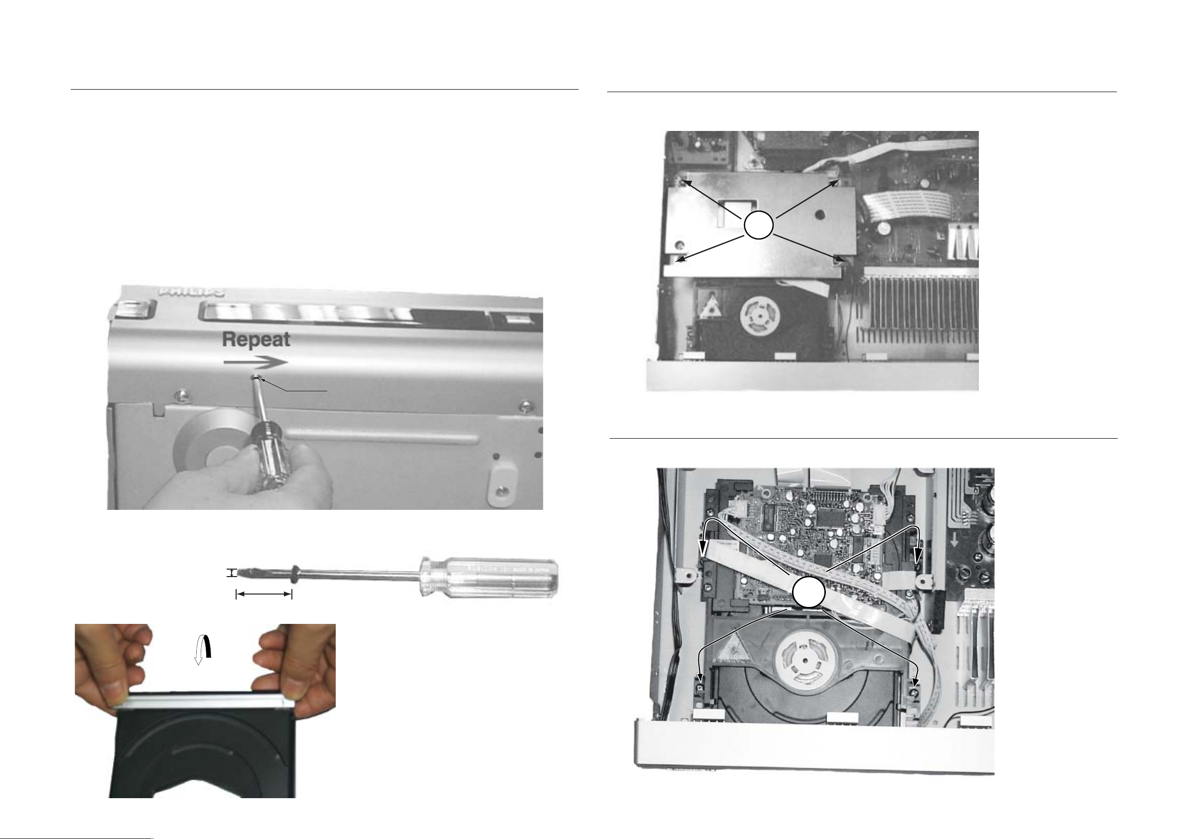
DISASSEMBLY INSTRUCTIONS
3-1
3-1
Dismantling of the Key Board Assembly
1) Open the DVD Tray by using the Open/Close Button
while the Set is ON and disconnect the mains supply after
removing the Tray Cover.
Note: If this is not possible, the DVD T ray has to be open
manually.
Take a mini screw driver about 2mm diameter and make
a marking 24mm from the tip as shown in figure 2. Place
the set on its side, insert the mini screw driver till the
marking and slide it towards the right as shown in figure
1 until the Tray moves out of the Front Panel.
2) Return the set to its upright position and remove the Tray
Cover as shown in Figure 3 and close the tray manually
by pushing it back in.
3) Loosen 11 screws and remove the T op Cover by lifting the
rear portion upwards before sliding it out towards the rear.
-7 screws on the back
-2 screws each on the left & right side
4) Loosen 7 screws & lift up the top edge of Front Panel
assembly to free some catches (see figure 3) before
sliding it out towards the front.
-5 screws on the bottom
-1 screw each on the left & right side
Dismantling of the MPEG Board
1) Loosen 4 screws A to remove the metal cover together
with MPEG board and remove the connector as shown in
figure 4.
A
Note: Do not lost the limited
between the MPEG
board and the servo
board
2mm
Figure 1
24mm
Marking just outside the
Marking just outside the
slot on the rear cabinet
slot on the rear cabinet
Figure 4
Dismantling of the DVD Module
1) Loosen 4 screws B to remove the DVD module as shown
in figure 5 .
B
Figure 2
Figure 3
Figure5
3-2
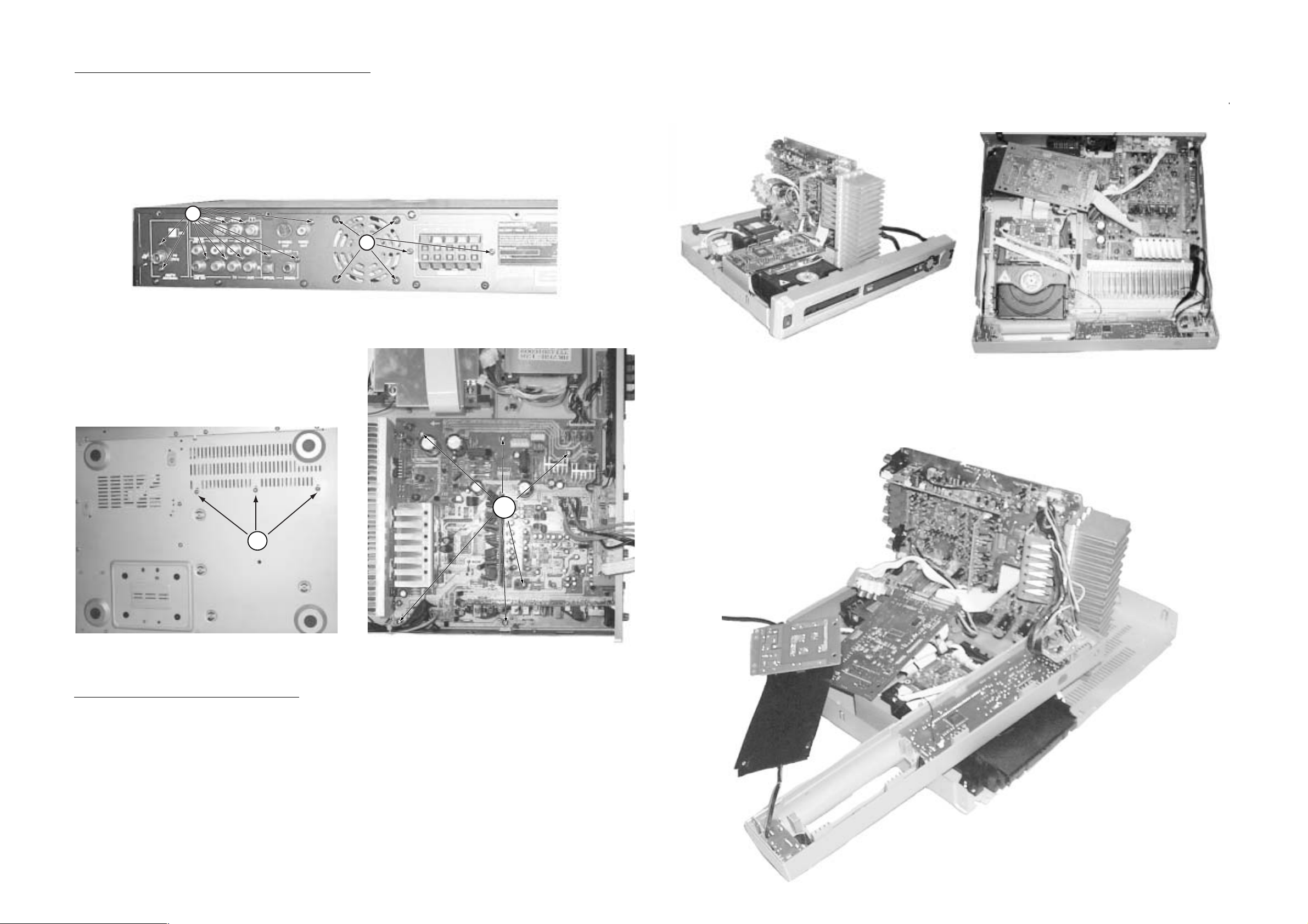
3-2
Dismantling of the Main Board (include Tuner & Surround Board)
1) Loosen 6 screws F on the top of main board as shown in figure 7.
2) Loosen 10 screws C at the back panel as shown in figure 8.
3) Loosen 3 screws D on the bottom cover as shown in figure 9.
4) Remove all connectors on tuner, surround, RGB & main board.
C
E
Figure 8
SERVICE POSITIONS
Service position A
Note: In some service positions the components or copper patterns of one board may risk touching its neighbouring pc
boards or metallic parts. T o prevent such short-circuit use a piece of hard paper or other insulating material between them.
Service position B
D
Figure 9
Dismantling of the Speaker Jack Board & Fan
1) Loosen 6 screws E at the back panel as shown in figure 8.
2) Remove all connectors at speaker jack and Fan.
Service position C
F
Figure 7
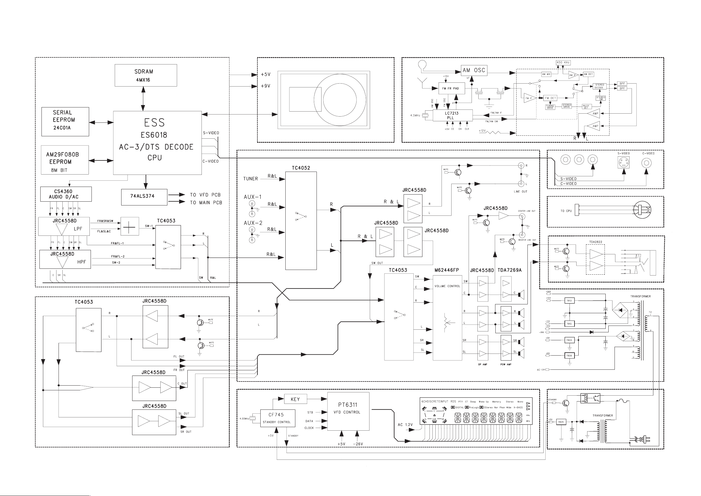
BLOCK DIAGRAM
MPEG PCB
4-1
4-1
TUNER PCB
Component
Video Out
DVD LOADER
MAIN PCB
Pr/Cr
Pb/Cb Y
Component Video Out
VOLUME PCB
EARPHONE PCB
RGB PCB
SURROUND PCB
KEY PCB
POWER PCB
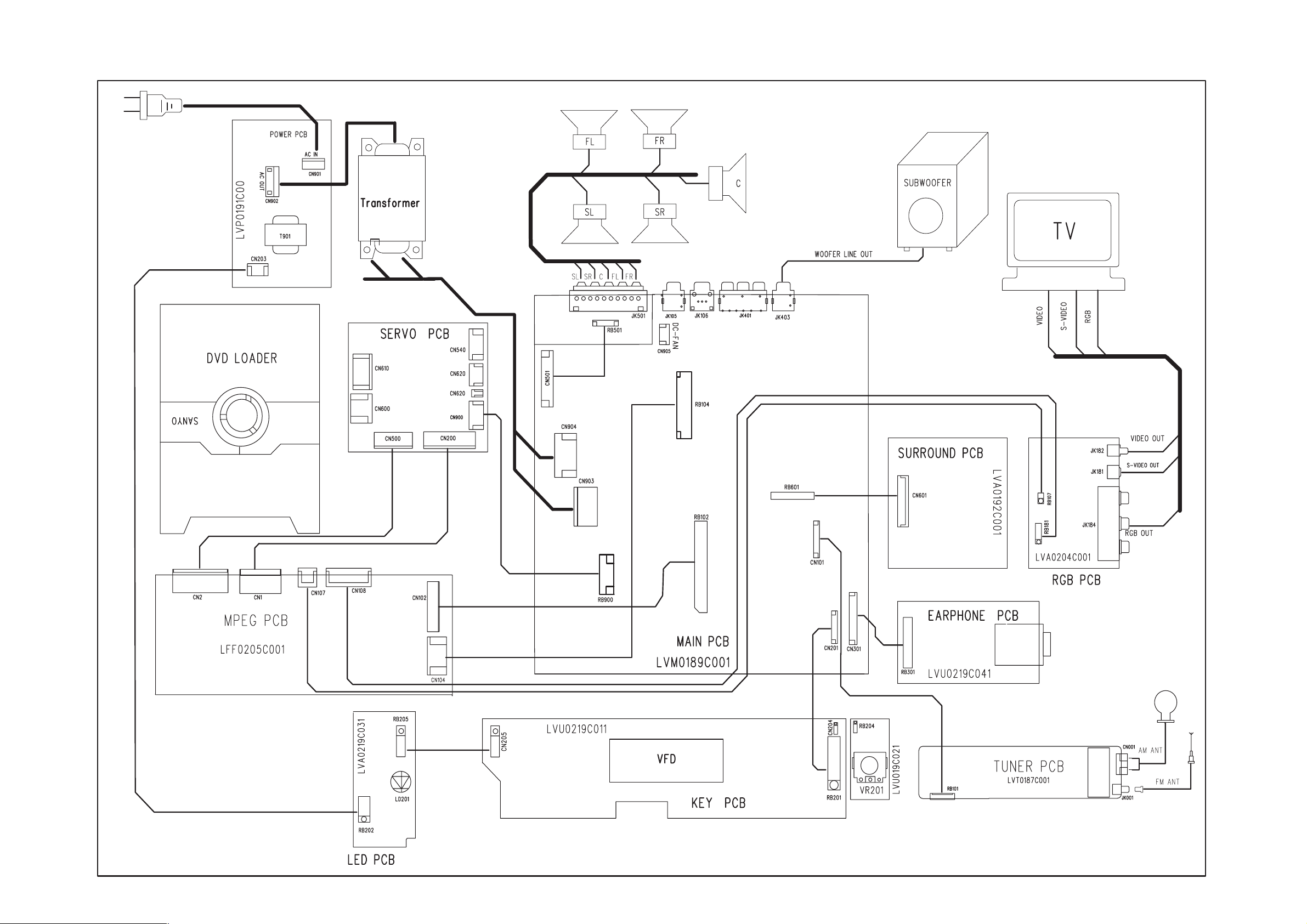
WIRING DIAGRAM
4-2
4-2
5-1
SR
5-1
FTD DISPLAY PIN ASSIGNMENT
3G 2G 1G
KEY / VOLUME / LED /
EARPHONE BOARD
TABLE OF CONTENTS
FTD Display Pin Assignment...........................................5-1
Pin Connection ................................................................5-1
Circuit Diagram ................................................................5-2
PCB Layout Top View ......................................................5-3
PCB Layout Bottom View ................................................5-3
Electrical Parts List ..........................................................5-4
L
SL
P1
P2
P3
P4
P5
P6
P7
P8
P9
P10
P11
P12
P13
P14
P15
P16
C
Sub
R
SR
4G 5G 6G 7G
8G 9G
f
g
rpn
e
(4G-11G)
1G 2G 3G 4G 5G 6G 7G 8G
Program
Sleep
DIGITAL
ProLogic
Ster eo
R
Sub
SR
C
L
SL
m
a
b
h
j
k
f
g
a
b
h
j
k
f
g
m
e
r
p
n
c
d
e
r
p
n
c
d
a
b
h
j
k
f
g
m
e
r
p
n
c
d
a
b
h
j
k
f
g
m
e
r
p
n
c
d
a
hjk
m
d
m
Col
10G 11G
b
c
9G
a
b
h
j
k
f
g
m
e
r
p
n
c
d
Dp
a
b
h
j
k
f
g
e
r
p
n
c
d
10G 11G
a
b
h
j
k
f
g
m
e
r
p
n
c
d
a
b
h
j
k
f
g
m
e
r
p
n
c
d
MHz
KHz
PIN CONNECTION
1
2
3
4
PIN NO.
F
CONNECTION
## Note ##
1. Fn: Filament pin
2. nG : Grid pin
3. Pn : Anode pin
4. NP : No Pin
5. NC : No Connection pin
F
1
2
5
N
1
2
P
G
G
6
7
8
9
1
1
1
1
1
1
1
1
1
1
2
2
2
2
2
2
2
2
2
2
3
3
3
3
3
3
0
1
2
3
4
5
6
7
8
9
0
1
2
3
4
5
6
7
8
9
0
1
2
3
4
5
3
4
5
6
7
8
9
10
11
N
N
P
P
P
P
P
P
P
P
P
P
P
P
P
P
P
P
N
F
F
G
G
G
G
G
G
G
G
G
C
C
1
2
3
4
5
6
7
8
9
10
11
12
13
14
15
16
P
2
2
CIRCUIT DIAGRAM - KEY BOARD
5-2
5-2
A
B
C
D
E
F
1
0v
4.9v
4.9v
2 3 4 5 6
5.1v
4.9v
0v
4.9v
0v
3.5v
3.5v
4.9v
0v
4.9v
5.1v
0v
5.1v
VOLUME SCHEMATIC
3.5v
4.9v
+5v
4.9v
4.9v
4.9v
0v
5.1v
4.2v
AC 1.3v
0v
AC 1.3v
4.9v
4.9v
4.9v
5.1v
0v
0v
LVU0219C021
LVU0219C031
LED SCHEMATIC
LVU0219C041
PHONE SCHEMATIC
C201 A1
C202 A1
C203 A1
C204 D3
C205 D3
A
C207 B1
C208 B1
C209 B1
C212 F2
C213 F2
C214 F4
C215 F4
C328 B6
B
C331 B6
C334 B6
C340 C6
C341 C6
C342 B5
C345 B5
C346 D6
C347 C6
C348 C6
C
C350 A6
C351 A6
C991 F3
C992 F2
C993 F2
C994 F2
D201 C3
D202 C3
D
D203 C3
D301 D6
D302 B6
D985 E3
DP201 A3
IC251 B2
IC304 B6
IC981 F3
E
JK301 A5
LD201 E4
Q201 D1
Q202 D2
Q203 D3
Q204 D4
Q306 C6
Q307 D5
F
Q308 B5
Q983 E2
R201 A1
R202 B1
R203 B1
R204 B1
R205 B1
R206 B1
R213 A1
R214 A2
R215 C5
R216 D3
R223 C4
R224 C4
R225 D3
R227 E3
R228 C1
R229 C1
R230 C1
R231 C1
R232 D2
R233 D2
R234 D2
R235 D2
R236 D3
R237 D3
R238 A1
R239 B1
R241 D4
R242 D4
R349 B6
R350 B6
R353 C6
R354 C6
R355 D6
R356 D6
R357 D6
R358 D6
R359 D6
R360 C6
R361 C6
R362 C5
R363 C6
R364 C6
R365 B6
R366 B6
R367 D6
R987 F2
R988 E2
R991 F3
R992 F3
R993 F3
R995 E3
R996 F2
R998 E2
R9002 D3
R9003 C4
R9004 E4
RB201 D5
RB202 F5
RB204 E4
RB205 F4
RB301 E6
SN201 C3
TA202 D1
TA204 C2
TA205 C2
TA206 C2
TA207 C2
TA208 D2
TA209 D2
TA210 F4
VR201 E5
XL981 F2
FB302 B6
FB303 B6
ZD201 C4
ZD202 D3
ZD203 D3
ZD301 B5
1 2 3 4 5 6
5-3 5-3
PCB LAYOUT TOP VIEW - KEY BOARD
A
B
C201 B1
C203 B2
C204 A4
C212 A2
C214 A5
C215 B5
C221 B3
C328 A6
C331 B6
C332 B6
C333 B6
C334 B5
C340 A6
C341 A6
C342 B6
C345 A6
C346 A5
C349 A6
C991 A4
CN204 A5
CN205 A1
D201 B3
D202 B4
D203 A2
D301 A6
D302 A6
D985 A3
DP201 A2
ED301 A6
FB302 B6
FB303 B6
IC304 B6
IC981 A3
JK301 B6
JW201 A1
JW202 A1
JW203 A2
JW204 B2
JW205 A2
JW206 A2
JW207 A3
JW208 A3
JW209 A3
JW210 A3
JW211 A3
JW212 B3
JW213 B3
JW214 B3
JW215 B3
JW216 A4
JW217 A3
JW218 A4
JW219 B4
JW220 B4
JW221 B4
JW222 A4
JW223 B4
JW224 A5
JW225 A3
JW226 B3
JW227 B1
JW228 B2
JW301 A6
JW302 A6
JW303 B6
JW304 B6
LD201 B1
Q306 A6
Q307 A5
Q308 A6
R204 B3
R205 B3
R206 B3
R214 B2
R216 A3
R223 A5
R224 A5
R225 A4
R227 A1
R228 B3
R231 B3
R234 A4
R236 A1
R238 A2
R239 A2
R240 A2
R242 B4
R349 A6
R350 A6
R353 A6
R354 A5
R355 A6
R356 A6
R357 A6
R358 A6
R359 A6
R360 B6
R361 A6
R362 A6
R363 A6
R364 A6
R365 B6
R366 B6
RB205 A1
RB301 A6
R991 A4
RB201 B5
RB202 B1
RB204 A5
SN201 A3
TA202 B5
TA204 A5
TA205 B4
TA206 B4
TA207 A4
TA208 A4
TA209 B1
TA210 A1
VR201 B5
XL981 A2
ZD201 B5
ZD202 A3
ZD203 A4
ZD301 A6
12 3 456
A
B
12 3 456
PCB LAYOUT BOTTOM VIEW - KEY BOARD
C202 A1
C203 B3
C205 B3
C207 B2
C208 B2
C209 B3
A
B
C213 B3
C216 A5
C217 B2
C218 B1
C219 A2
C220 A2
C222 A2
C347 B6
C348 B6
C350 A6
C351 A6
C992 B2
C993 B2
C994 B2
IC251 B2
Q201 A4
Q202 A4
Q203 B1
12 3 456
Q204 B4
Q983 B3
R201 B2
R202 B2
R203 B2
R213 B2
R215 B5
R229 A3
R230 A3
R233 A4
R232 A4
R235 A4
R237 B1
R241 A4
R367 B6
R987 B3
R988 B3
R993 B3
R994 B3
R992 B3
R995 B3
R996 B3
R998 B3
R9002 B4
R9003 B5
R9004 B4
A
B
12 3 456

5-4
5-4
ELECTRICAL PARTS LIST - KEY, VOLUME, LED & EARPHONE BOARD
MISCELLANEOUS
DP201 9965 000 12538 VFD DISPLAY
JK301 9965 000 12505 CINCH SOCKET 6P WHITE/RED
SN201 9965 000 13071 IRT SENSOR IRM-2038F4 W/GND
TA202 4822 276 13648 TACT SWITCH
TA204 4822 276 13648 TACT SWITCH
TA205 4822 276 13648 TACT SWITCH
TA206 4822 276 13648 TACT SWITCH
TA207 4822 276 13648 TACT SWITCH
TA208 4822 276 13648 TACT SWITCH
TA209 4822 276 13648 TACT SWITCH
TA210 4822 276 13648 TACT SWITCH
VR201 9965 000 12539 ROTARY ENCODER EC16B24-204
XL981 9965 000 12540 CRYSTAL 4,00MHZ
CAPACITORS
C201 9965 000 12541 100UF 16V 20%
C202 9965 000 14136 0,1UF 50V 20%
C203 9965 000 12543 100UF 35V 20%
C204 9965 000 12541 100UF 16V 20%
C205 9965 000 14136 0,1UF 50V 20%
C207 4822 126 13486 15PF 2% 63V
C208 4822 126 13486 15PF 2% 63V
C209 4822 126 13486 15PF 2% 63V
C212 9965 000 12559 100UF 16V 20%
C213 9965 000 14136 0,1UF 50V 20%
C214 9965 000 12546 27PF 50V 5%
C215 9965 000 12546 27PF 50V 5%
C216 9965 000 14136 0,1UF 50V 20%
C217 9965 000 14136 0,1UF 50V 20%
C218 9965 000 14136 0,1UF 50V 20%
C219 9965 000 14136 0,1UF 50V 20%
C220 9965 000 14659 0,068UF 50V 20%
C221 9965 000 13094 0,068UF 50V 10%
C222 9965 000 14136 0,1UF 50V 20%
C224 9965 000 14676 0,0068UF 50V 10%
C328 9965 000 14660 10UF 25V 20%
C331 9965 000 12541 100UF 16V 20%
C332 9965 000 12541 100UF 16V 20%
C333 9965 000 12541 100UF 16V 20%
C334 9965 000 12541 100UF 16V 20%
C340 9965 000 12583 1UF 50V 20%
C341 9965 000 12583 1UF 50V 20%
C342 9965 000 12541 100UF 16V 20%
C345 9965 000 14661 220UF 16V 20%
C346 9965 000 14662 4,7UF 50V 20%
C347 9965 000 12478 4700PF 50V 20%
C348 9965 000 12478 4700PF 50V 20%
C349 9965 000 14663 0,1UF 50V +80/-20%
C350 9965 000 14136 0,1UF 50V 20%
C351 9965 000 14220 0,1UF 50V 10%
C991 9965 000 12547 10UF 50V 20%
C992 5322 122 32658 22PF 5% 50V
C993 5322 122 32658 22PF 5% 50V
C994 4822 126 13692 47PF 1% 63V
RESISTORS
R201 9965 000 12484 10K 1/10W 5%
R202 9965 000 12484 10K 1/10W 5%
R203 9965 000 12484 10K 1/10W 5%
R204 4822 050 21001 100R 1% 0,6W
R205 4822 050 21001 100R 1% 0,6W
R206 4822 050 21001 100R 1% 0,6W
R213 4822 051 20472 4K7 5% 0,1W
R214 9965 000 12560 56K 1/6W 5%
R215 4822 051 20223 22K 5% 0,1W
R216 4822 050 21001 100R 1% 0,6W
R223 4822 050 21003 10K 1% 0,6W
R224 4822 050 21003 10K 1% 0,6W
R225 9965 000 12549 220R 1/6W 5%
R227 4822 050 25601 560R 1% 0,6W
R228 4822 050 21003 10K 1% 0,6W
R229 9965 000 12484 10K 1/10W 5%
R230 9965 000 12484 10K 1/10W 5%
R231 4822 050 21003 10K 1% 0,6W
R232 4822 051 20223 22K 5% 0,1W
R233 4822 117 10837 100K 1% 0,1W
R234 4822 050 22203 22K 1% 0,6W
R235 4822 117 10837 100K 1% 0,1W
R236 4822 050 22203 22K 1% 0,6W
R237 4822 117 10837 100K 1% 0,1W
R238 9965 000 12515 2,2K 1/6W 5%
R239 9965 000 12515 2,2K 1/6W 5%
R240 9965 000 12515 2,2K 1/6W 5%
R241 4822 117 11449 2K2 5% 0,1W
R242 9965 000 12515 2,2K 1/6W 5%
R349 4822 050 21003 10K 1% 0,6W
R350 9965 000 12560 56K 1/6W 5%
R353 4822 050 24703 47K 1% 0,6W
R354 4822 050 24703 47K 1% 0,6W
R355 9965 000 12631 180K 1/6W 5%
R356 9965 000 12519 1K 1/6W 5%
R357 9965 000 12631 180K 1/6W 5%
R358 9965 000 12519 1K 1/6W 5%
R359 4822 050 22203 22K 1% 0,6W
R360 9965 000 14664 180R 1/6W 5%
R361 9965 000 14664 180R 1/6W 5%
R362 4822 050 21502 1K5 1% 0,6W
R363 9965 000 14665 3K 1/6W 5%
R364 9965 000 14665 3K 1/6W 5%
R365 9965 000 12519 1K 1/6W 5%
R366 9965 000 12519 1K 1/6W 5%
R367 9965 000 12482 47K 1/10W 5%
R987 4822 117 11373 100R 1% 1/10W
R988 4822 051 20472 4K7 5% 0,1W
ELECTRICAL PARTS LIST - KEY, VOLUME, LED & EARPHONE BOARD
R991 4822 050 21003 10K 1% 0,6W
R992 9965 000 12484 10K 1/10W 5%
R993 9965 000 12484 10K 1/10W 5%
R994 9965 000 12484 10K 1/10W 5%
R995 9965 000 12484 10K 1/10W 5%
R996 4822 117 10837 100K 1% 0,1W
R998 9965 000 12484 10K 1/10W 5%
R9002 9965 000 12482 47K 1/10W 5%
R9003 9965 000 12484 10K 1/10W 5%
R9004 4822 051 20102 1K 5% 0,1W
COILS & FILTERS
FB302 9965 000 12470 BEAD FERITE 100R AT 100MHZ
FB303 9965 000 12470 BEAD FERITE 100R AT 100MHZ
DIODES
D201 4822 130 30621 1N4148
D202 4822 130 30621 1N4148
D203 4822 130 30621 1N4148
D301 4822 130 30621 1N4148
D302 4822 130 30621 1N4148
D985 4822 130 30621 1N4148
LD201 9965 000 12537 LED 3 DIA RED ROUND
ZD201 9965 000 12554 ZENER 3,8-4,0V 0,5W
ZD202 4822 130 34233 BZX79-B5V1
ZD203 4822 130 34233 BZX79-B5V1
ZD301 4822 130 80272 MTZJ7,5C
TRANSISTORS & INTEGRATED CIRCUITS
IC251 9965 000 12550 PT6311(PTC)
IC304 9965 000 12563 TDA2822
IC981 9965 000 12551 CF745
Q201 9965 000 14175 2SA733Q,P
Q202 9965 000 14175 2SA733Q,P
Q203 9965 000 14175 2SA733Q,P
Q204 9965 000 09584 2SC945
Q306 4822 130 43818 2SC2878-A
Q307 4822 130 43818 2SC2878-A
Q308 4822 130 41651 2SC2001L
Q983 9965 000 14175 2SA733Q,P
Note: Only the parts mentioned in this list are normal service spare
parts.
6-1
6-1
TUNER ADJUSTMENT TABLE
Waverange Input frequency Input Tuned to Adjust Output Scope/Voltmeter
VARICAP ALIGNMENT
TUNER BOARD
TABLE OF CONTENTS
FM
87.5 - 108MHz
(50kHz grid)
AM
531 - 1602kHz
(9kHz grid)
( 22S / 30S / 21R /
21H / 33S / 35S )
AM
530-1700kHz
(10kHz grid)
( 21L / 21L / 37S )
FM - IF
FM
FM - RF
FM
AM IF
10.7MHz, 50mV
continuous wave
108MHz
87.5MHz
A
mod=1kHz
∆f= ±22.5kHz
108MHz
87.5MHz
1602KHz
531KHz
1700KHz
530KHz
IC 101
short circuit
to block AFC
108MHz
87.5MHz
5130
check
TC002
T003
1
TC002
T003
23
200P
T105
2F
6.5V ±1.2V
1.5V ±0.5V
7.8V ±0.2V
±
1.1V ±0.2V
8.0V 0.2V
1.1V 0.2V
±
fo
Symmetric
Max
MAX
Tuner Adjustment Table ..................................................................6-1
Block Diagram ................................................................................6-2
Circuit Diagram...............................................................................6-3
PCB Layout Top View..................................................................... 6-4
PCB Layout Bottom View ............................................................... 6-5
Electrical Parts List.........................................................................6-6
AM
AM AFC
MW
AM RF
MW
MW
IC 101
24
R220
100nF
T102
4
f
symmetric
max.
o
450kHz
Connect pin 29 of
IC 101 (AM Osc.)
C
∆f = ±15kHz
V
= 3mV
RF
with short wire to
ground (pin 28)
3)
1557kHz TC001
1557kHz
B
1650kHz
580kHz
∆f = ±30kHz
as low as
V
RF
possible
576kHz576kHz
1650kHz
580kHz
T002
TC001
T002
max.
4
f
o
symmetric
Use Service Testprogram. By selecting the TUNER TEST test frequencies will be stored as preset frequencies automatically.
1)
If sensitivity of frequency counter is too low adjust to max. channel separation
(input signal: stereo left 90% + 9%, adjust output on right channel to minimum)
3)
For AM RF adjustments the original frame antenna has to be used!
2)
RC network serves for damping the IF-filter while
adjusting the other one.
Loading...