


MOTOROLA TL084CN, TL082CDR2, TL082CD, TL082ACP, TL081CDR2 Datasheet
...
JFET Input Operational
Amplifiers
These low±cost JFET input operational amplifiers combine two state±of± the±art linear technologies on a single monolithic integrated circuit. Each internally compensated operational amplifier has well matched high voltage JFET input devices for low input offset voltage. The BIFET technology provides wide bandwidths and fast slew rates with low input bias currents, input offset currents, and supply currents.
These devices are available in single, dual and quad operational amplifiers which are pin±compatible with the industry standard MC1741, MC1458, and the MC3403/LM324 bipolar products.
•Input Offset Voltage Options of 6.0 mV and 15 mV Max
•Low Input Bias Current: 30 pA
•Low Input Offset Current: 5.0 pA
•Wide Gain Bandwidth: 4.0 MHz
•High Slew Rate: 13 V/μs
•Low Supply Current: 1.4 mA per Amplifier
•High Input Impedance: 1012 Ω
ORDERING INFORMATION
Op Amp |
|
Operating |
|
|
Function |
Device |
Temperature Range |
Package |
|
|
|
|
|
|
Single |
TL081CD |
TA = 0° to +70°C |
SO±8 |
|
|
|
|||
TL081ACP |
Plastic DIP |
|||
|
|
|||
|
|
|
|
|
Dual |
TL082CD |
TA = 0° to +70°C |
SO±8 |
|
|
|
|||
TL082ACP |
Plastic DIP |
|||
|
|
|||
|
|
|
|
|
Quad |
TL084CN, ACN |
TA = 0° to +70°C |
Plastic DIP |
|
Representative Circuit Schematic (Each Amplifier) |
|
|||||||
|
|
|
|
|
|
Output |
|
|
VCC |
|
|
|
|
|
|
|
|
|
|
|
|
Q3 |
Q4 |
|
Q5 |
Q2 |
Q1 |
|
|
|
|
|
|
|
|
|
|
||
|
J1 |
J2 |
|
|
|
Q6 |
|
|
|
± |
|
|
|
|
|
|
|
||
Inputs |
|
|
|
|
|
|
2.0 k |
|
|
+ |
|
|
|
Q17 |
|
|
|
|
|
|
|
|
|
|
Q20 |
|
|
J3 |
|
|
|
|
|
|
|
Q23 |
|
|
|
|
|
|
Q15 |
|
Q19 |
|
|
|
|
|
|
|
10 pF |
24 |
|
|
|
||
|
|
|
|
|
|
|
|
||
|
|
Q14 |
|
|
|
|
|
|
|
|
|
|
|
|
|
|
|
|
|
|
|
|
|
|
Q21 Q22 |
Q24 |
|
|
|
|
Q12 |
|
Q13 |
Q16 |
|
|
|
|
|
|
Q10 |
Q11 |
|
|
Q9 |
Q8 |
Q25 |
|
|
|
|
|
|
|
|
|
Q7 |
|
|
|
|
|
|
|
|
|
|
|
|
Offset |
|
Q18 |
|
|
|
|
|
|
|
|
|
|
|
|
|
|
|
|
|
Null |
1.5 k |
1.5 k |
|
|
|
|
|
|
|
(TL081 |
|
|
|
|
|
|
|
||
|
|
|
|
|
|
|
|
|
|
only) |
|
|
|
|
|
|
|
Bias Circuitry |
VEE |
|
|
|
|
|
|
|
|
||
|
|
|
|
|
|
|
|
Common to All |
|
|
|
|
|
|
|
|
|
Amplifiers |
|
Order this document by TL081C/D
TL081C,AC
TL082C,AC
TL084C,AC
JFET INPUT
OPERATIONAL AMPLIFIERS
SEMICONDUCTOR
TECHNICAL DATA
|
8 |
8 |
1 |
1 |
|
P SUFFIX |
D SUFFIX |
PLASTIC PACKAGE |
PLASTIC PACKAGE |
CASE 626 |
CASE 751 |
|
(SO±8) |
PIN CONNECTIONS
Offset Null |
1 |
|
8 |
NC |
Inv + Input |
2 |
|
7 |
VCC |
Noninvt Input |
3 |
+ |
6 |
Output |
VEE |
4 |
|
5 |
Offset Null |
|
TL081 (Top View) |
|
||
Output A |
1 |
|
8 |
VCC |
Inputs A |
2 |
± |
7 |
Output B |
3 |
+ |
6 |
|
|
|
± |
Inputs B |
||
VEE |
4 |
+ |
5 |
|
|
|
|||
|
TL082 (Top View) |
|
||
N SUFFIX
PLASTIC PACKAGE
CASE 646
14
1
PIN CONNECTIONS
Output 1 |
1 |
|
|
|
|
14 |
Output 4 |
|
Inputs 1 |
2 |
± |
|
|
± |
13 |
Inputs 4 |
|
|
+ |
1 |
4 |
+ |
|
|||
|
3 |
12 |
|
|||||
VCC |
4 |
|
|
|
|
11 |
VEE |
|
Inputs 2 |
5 |
+ |
|
|
+ |
10 |
Inputs 3 |
|
6 |
± |
2 |
3 |
± |
9 |
|||
|
|
|||||||
|
|
|
|
|
|
|||
Output 2 |
7 |
|
|
|
|
8 |
Output 3 |
TL084 (Top View)
Motorola, Inc. 1997 |
Rev 1 |
TL081C,AC TL082C,AC TL084C,AC
MAXIMUM RATINGS
Rating |
Symbol |
Value |
Unit |
|
|
|
|
Supply Voltage |
VCC |
18 |
V |
|
VEE |
±18 |
|
Differential Input Voltage |
VID |
±30 |
V |
Input Voltage Range (Note 1) |
VIDR |
±15 |
V |
Output Short Circuit Duration (Note 2) |
tSC |
Continuous |
|
Power Dissipation |
|
|
|
Plastic Package (N, P) |
PD |
680 |
mW |
Derate above TA = +47°C |
1/θJA |
10 |
mW/°C |
Operating Ambient Temperature Range |
TA |
0 to +70 |
°C |
Storage Temperature Range |
Tstg |
±65 to +150 |
°C |
NOTES: 1. The magnitude of the input voltage must not exceed the magnitude of the supply voltage or 15 V, whichever is less.
2.The output may be shorted to ground or either supply. Temperature and/or supply voltages must be limited to ensure that power dissipation ratings are not exceeded.
3.ESD data available upon request.
ELECTRICAL CHARACTERISTICS (VCC = 15 V, VEE = ±15 V, TA = Tlow to Thigh [Note 1].)
|
Characteristics |
Symbol |
Min |
Typ |
Max |
Unit |
|
|
|
|
|
|
|
Input Offset Voltage (RS ≤ 10 k, VCM = 0) |
VIO |
|
|
|
mV |
|
TL081C, TL082C |
|
± |
± |
20 |
|
|
TL084C |
|
± |
± |
20 |
|
|
TL08_AC |
|
± |
± |
7.5 |
|
|
|
|
|
|
|
|
|
Input Offset Current (VCM = 0) (Note 2) |
IIO |
|
|
|
nA |
|
TL08_C |
|
± |
± |
5.0 |
|
|
TL08_AC |
|
± |
± |
3.0 |
|
|
|
|
|
|
|
|
|
Input Bias Current (VCM = 0) (Note 2) |
IIB |
|
|
|
nA |
|
TL08_C |
|
± |
± |
10 |
|
|
TL08_AC |
|
± |
± |
7.0 |
|
|
|
|
|
|
|
|
|
Large±Signal Voltage Gain (VO= ±10 V,RL ≥ 2.0 k) |
AVOL |
|
|
|
V/mV |
|
TL08_C |
|
15 |
± |
± |
|
|
TL08_AC |
|
25 |
± |
± |
|
|
|
|
|
|
|
|
|
Output Voltage Swing (Peak±to±Peak) |
VO |
|
|
|
V |
|
(RL ≥ |
10 k) |
|
24 |
± |
± |
|
(RL ≥ |
2.0 k) |
|
20 |
± |
± |
|
NOTES: 1. Tlow = 0°C for TL081AC,C TL082AC,C TL084AC,C
Thigh = 70°C for TL081AC TL082AC,C
TL084AC,C
2.Input Bias currents of JFET input op amps approximately double for every 10°C rise in Junction Temperature as shown in Figure 3. To maintain junction temperature as close to ambient temperature as possible, pulse techniques must be used during testing.
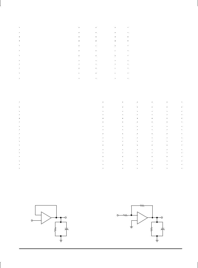
Figure 1. Unity Gain Voltage Follower |
Figure 2. Inverting Gain of 10 Amplifier |
||
|
|
10 k |
|
± |
|
1.0 k |
|
VO |
± |
VO |
|
+ |
Vin |
||
|
+ |
|
|
Vin |
|
|
|
RL = 2.0 k |
CL = 100 pF |
RL |
CL = 100 pF |
2 |
MOTOROLA ANALOG IC DEVICE DATA |

TL081C,AC TL082C,AC TL084C,AC
ELECTRICAL CHARACTERISTICS (VCC = 15 V, VEE = ±15 V, TA = 25°C, unless otherwise noted.)
Characteristics |
|
|
Symbol |
Min |
Typ |
Max |
Unit |
|||
|
|
|
|
|
|
|
|
|
|
|
Input Offset Voltage (RS ≤ 10 k, VCM = 0) |
|
|
VIO |
|
|
|
mV |
|||
TL081C, TL082C |
|
|
|
|
± |
5.0 |
15 |
|
|
|
TL084C |
|
|
|
|
± |
5.0 |
15 |
|
|
|
TL08_AC |
|
|
|
|
± |
3.0 |
6.0 |
|
|
|
|
|
|
|
|
|
|
|
|||
Average Temperature Coefficient of Input Offset Voltage |
VIO/ T |
± |
10 |
± |
μV/°C |
|||||
RS = 50 Ω, TA = Tlow to Thigh (Note 1) |
|
|
|
|
|
|
|
|
|
|
Input Offset Current (VCM = 0) (Note 2) |
|
|
IIO |
|
|
|
pA |
|||
TL08_C |
|
|
|
|
± |
5.0 |
200 |
|
|
|
TL08_AC |
|
|
|
|
± |
5.0 |
100 |
|
|
|
|
|
|
|
|
|
|
|
|
|
|
Input Bias Current (VCM = 0) (Note 2) |
|
|
|
IIB |
|
|
|
pA |
||
TL08_C |
|
|
|
|
± |
30 |
400 |
|
|
|
TL08_AC |
|
|
|
|
± |
30 |
200 |
|
|
|
|
|
|
|
|
|
|
|
|
|
|
Input Resistance |
|
|
|
ri |
± |
1012 |
± |
Ω |
||
Common Mode Input Voltage Range |
|
|
|
VICR |
±10 |
|
|
V |
||
TL08_C |
|
|
|
|
15, ±12 |
± |
|
|
|
|
TL08_AC |
|
|
|
|
±11 |
15, ±12 |
± |
|
|
|
|
|
|
|
|
|
|
|
|
|
|
Large Signal Voltage Gain (VO = ±10 V, RL ≥ |
2.0 k) |
|
AVOL |
|
|
|
V/mV |
|||
TL08_C |
|
|
|
|
25 |
150 |
± |
|
|
|
TL08_AC |
|
|
|
|
50 |
150 |
± |
|
|
|
|
|
|
|
|
|
|
|
|
|
|
Output Voltage Swing (Peak±to±Peak) |
|
|
|
VO |
24 |
28 |
± |
V |
||
(RL = 10 k) |
|
|
|
|
|
|
|
|
|
|
Common Mode Rejection Ratio (RS ≤ 10 k) |
|
|
CMRR |
|
|
|
dB |
|||
TL08_C |
|
|
|
|
70 |
100 |
± |
|
|
|
TL08_AC |
|
|
|
|
80 |
100 |
± |
|
|
|
|
|
|
|
|
|
|
|
|
|
|
Supply Voltage Rejection Ratio (RS ≤ 10 k) |
|
|
PSRR |
|
|
|
dB |
|||
TL08_C |
|
|
|
|
70 |
100 |
± |
|
|
|
TL08_AC |
|
|
|
|
80 |
100 |
± |
|
|
|
|
|
|
|
|
|
|
|
|
|
|
Supply Current (Each Amplifier) |
|
|
|
ID |
± |
1.4 |
2.8 |
mA |
||
Unity Gain Bandwidth |
|
|
|
BW |
± |
4.0 |
± |
MHz |
||
|
|
|
|
|
|
|
|
|
|
|
Slew Rate (See Figure 1) |
|
|
|
SR |
± |
13 |
± |
V/μs |
||
Vin = 10 V, RL = 2.0 k, CL = 100 pF |
|
|
|
|
|
|
|
|
|
|
Rise Time (See Figure 1) |
|
|
|
tr |
± |
0.1 |
± |
μs |
||
Overshoot (Vin = 20 mV, RL = 2.0 k, CL = 100 pF) |
|
OS |
± |
10 |
± |
% |
|
|
||
Equivalent Input Noise Voltage |
|
|
|
en |
± |
25 |
± |
nV/√ |
|
|
|
|
|
Hz |
|||||||
RS = 100 Ω, f = 1000 Hz |
|
|
|
|
|
|
|
|
|
|
Channel Separation |
|
|
|
CS |
± |
120 |
± |
dB |
||
AV = 100 |
|
|
|
|
|
|
|
|
|
|
NOTES: 1. Tlow = 0°C for TL081AC,C |
Thigh |
= 70°C for TL081AC |
|
|
|
|
|
|
|
|
TL082AC,C |
|
|
TL082AC,C |
|
|
|
|
|
|
|
TL084AC,C |
|
|
TL084AC,C |
|
|
|
|
|
|
|
2.Input Bias currents of JFET input op amps approximately double for every 10°C rise in Junction Temperature as shown in Figure 3. To maintain junction temperature as close to ambient temperature as possible, pulse techniques must be used during testing.
MOTOROLA ANALOG IC DEVICE DATA |
3 |
|
 Loading...