


TL062VP
MOTOROLA TL062VP, TL062VDR2, TL064ACDR2, TL064ACD, TL064CN Datasheet
...
SEMICONDUCTOR
TECHNICAL DATA
LOW POWER JFET INPUT
OPERATIONAL AMPLIFIERS
Order this document by TL062/D
D SUFFIX
PLASTIC PACKAGE
CASE 751
(SO–8)
P SUFFIX
PLASTIC PACKAGE
CASE 626
D SUFFIX
PLASTIC PACKAGE
CASE 751A
(SO–14)
N SUFFIX
PLASTIC PACKAGE
CASE 646
8
1
1
8
14
1
14
1
DUAL
PIN CONNECTIONS
(Top View)
QUAD
PIN CONNECTIONS
(Top View)
4
23
1
*
V
EE
Inputs 1
Output 1
Inputs 1
Output 1
V
CC
Inputs 2
Output 2
Inputs 2
Output 2
V
CC
Output 4
Inputs 4
V
EE
Inputs 3
Output 3
–
+
1
2
3
4
8
7
6
5
–
+
1
2
3
4
5
6
78
9
10
11
12
13
14
+
*
+
+
–
+
–
1
MOTOROLA ANALOG IC DEVICE DATA
These JFET input operational amplifiers are designed for low power
applications. They feature high input impedance, low input bias current and
low input offset current. Advanced design techniques allow for higher slew
rates, gain bandwidth products and output swing.
The commercial and vehicular devices are available in Plastic dual in–line
and SOIC packages.
• Low Supply Current: 200 µA/Amplifier
• Low Input Bias Current: 5.0 pA
• High Gain Bandwidth: 2.0 MHz
• High Slew Rate: 6.0 V/µs
• High Input Impedance: 10
12
Ω
• Large Output Voltage Swing:±14 V
• Output Short Circuit Protection
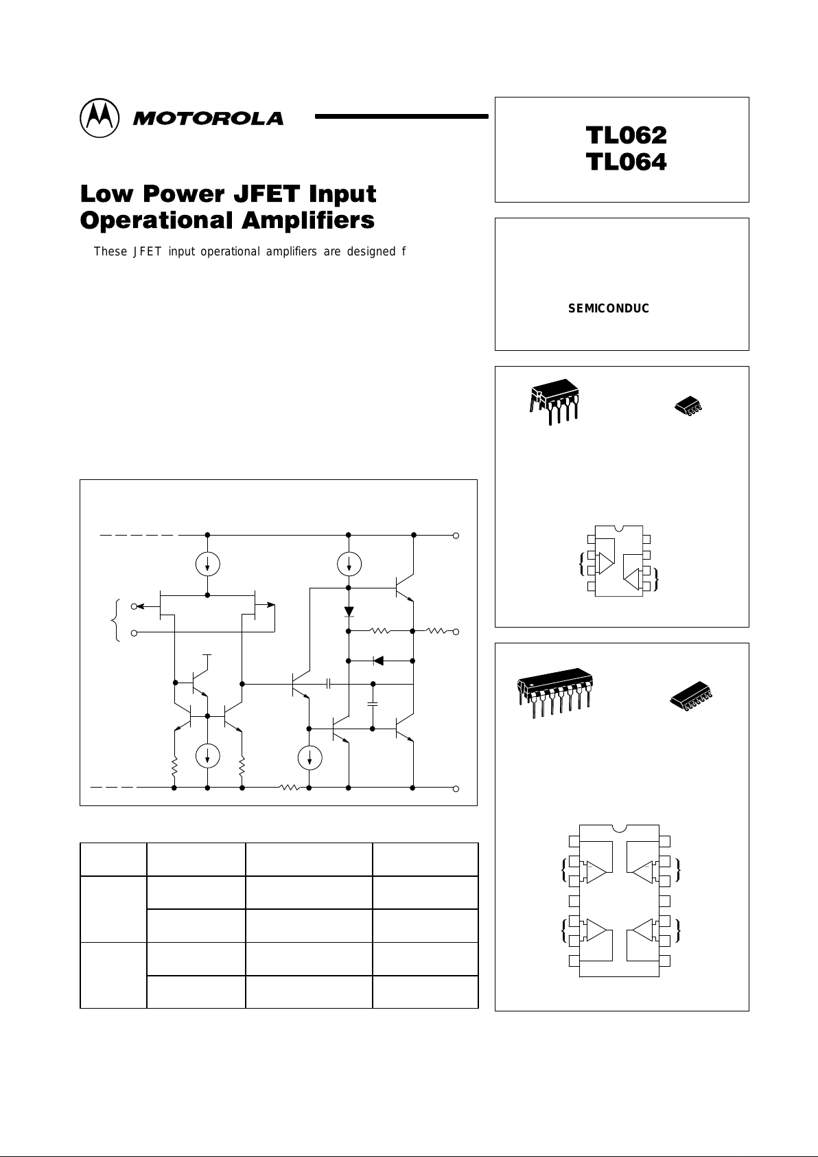
Representative Schematic Diagram
(Each Amplifier)
+
Q3
Q2Q1
–
+
R2
R5
J1
J2
R1
Q4
C1
Q5
D2
R3
Q7
R4
V
CC
Output
D1
C2
Q6
V
EE
Inputs
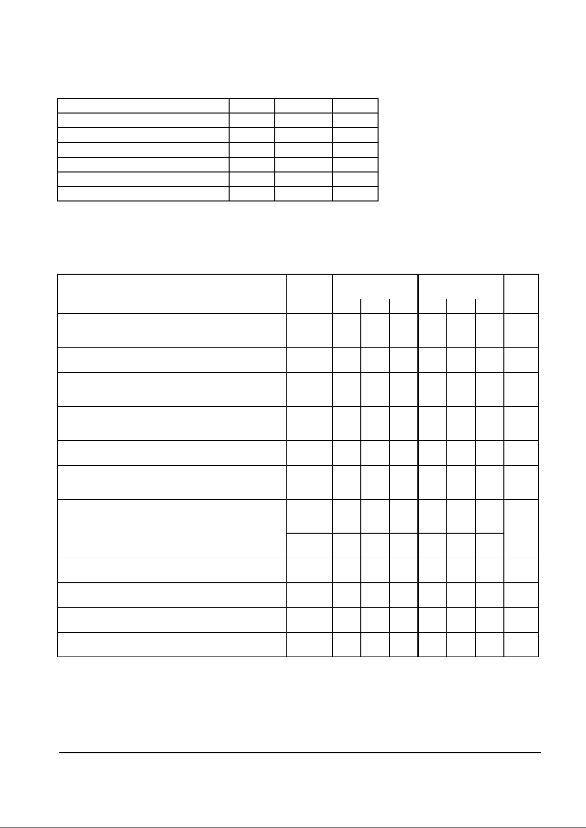
ORDERING INFORMATION
Op Amp
Function
Device
Operating
Temperature Range
Package
TL062CD, ACD
TL062CP, ACP
TA = 0° to +70°C
SO–8
Plastic DIP
Dual TL062VD
TL062VP
TA = –40° to +85°C
SO–8
Plastic DIP
TL064CD, ACD
TL064CN, ACN
TA = 0° to +70°C
SO–14
Plastic DIP
Quad TL064VD
TL064VN
TA = –40° to +85°C
SO–14
Plastic DIP
Motorola, Inc. 1996 Rev 5
TL062 TL064
2
MOTOROLA ANALOG IC DEVICE DATA
MAXIMUM RATINGS
Rating Symbol Value Unit
Supply Voltage (from VCC to VEE) V
S
+36 V
Input Differential Voltage Range (Note 1) V
IDR
±30 V
Input Voltage Range (Notes 1 and 2) V
IR
±15 V
Output Short Circuit Duration (Note 3) t
SC
Indefinite sec
Operating Junction Temperature T
J
+150 °C
Storage Temperature Range T
stg
–60 to +150 °C
NOTES: 1. Differential voltages are at the noninverting input terminal with respect to the inverting input
terminal.
2.The magnitude of the input voltage must never exceed the magnitude of the supply or 15 V,
whichever is less.
3.Power dissipation must be considered to ensure maximum junction temperature (TJ) is not
exceeded. (See Figure 1.)
ELECTRICAL CHARACTERISTICS (V
CC
= +15 V , VEE = –15 V , TA = 0° to +70°C, unless otherwise noted.)
TL062AC
TL064AC
TL062C
TL064C
Characteristics Symbol Min Typ Max Min Typ Max Unit
Input Offset Voltage (RS = 50 Ω, VO = 0V)
TA = 25°C
TA = 0° to +70°C
V
IO
——3.0—6.0
7.5——
3.0—15
20
mV
Average Temperature Coefficient for Offset V oltage
(RS = 50 Ω, VO = 0 V)
∆VIO/∆T — 10 — — 10 — µV/°C
Input Offset Current (VCM = 0 V, VO = 0 V)
TA = 25°C
TA = 0° to +70°C
I
IO
——0.5—100
2.0——
0.5—200
2.0
pA
nA
Input Bias Current (VCM = 0 V, VO = 0 V)
TA = 25°C
TA = 0° to +70°C
I
IB
——3.0—200
2.0——
3.0—200
10
pA
nA
Input Common Mode Voltage Range
TA = 25°C
V
ICR
—
–11.5
+14.5
–12.0
+11.5——
–11
+14.5
–12.0
+11
—
V
Large Signal Voltage Gain (RL = 10 kΩ, VO = ±10 V)
TA = 25°C
TA = 0° to +70°C
A
VOL
4.0
4.058—
——3.0
3.058—
—
—
V/mV
Output Voltage Swing (RL = 10 kΩ, VID = 1.0 V)
TA = 25°C
VO+
VO–
+10—+14
–14—–10
+10—+14
–14—–10
V
TA = 0° to +70°C VO+
VO–
+10——
——–10
+10——
——–10
Common Mode Rejection
(RS = 50 Ω, VCM = V
ICR
min, VO = 0 V, TA = 25°C)
CMR 80 84 — 70 84 — dB
Power Supply Rejection
(RS = 50 Ω, VCM = 0 V, VO = 0, TA = 25°C)
PSR 80 86 — 70 86 — dB
Power Supply Current (each amplifier)
(No Load, VO = 0 V, TA = 25°C)
I
D
— 200 250 — 200 250 µA
Total Power Dissipation (each amplifier)
(No Load, VO = 0 V, TA = 25°C)
P
D
— 6.0 7.5 — 6.0 7.5 mW

TL062 TL064
3
MOTOROLA ANALOG IC DEVICE DATA
DC ELECTRICAL CHARACTERISTICS (V
CC
= +15 V , VEE = –15 V , TA = T
low
to T
high
[Note 4], unless otherwise noted.)
TL062V TL064V
Characteristics Symbol Min Typ Max Min Typ Max Unit
Input Offset Voltage (RS = 50 Ω, VO = 0V)
TA = 25°C
TA = T
low
to T
high
V
IO
——3.0—6.0
9.0——
3.0—9.0
15
mV
Average Temperature Coefficient for Offset V oltage
(RS = 50 Ω, VO = 0 V)
∆VIO/∆T
— 10 — — 10 —
µV/°C
Input Offset Current (VCM = 0 V, VO = 0 V)
TA = 25°C
TA = T
low
to T
high
I
IO
——5.0—10020——5.0—100
20
pA
nA
Input Bias Current (VCM = 0 V, VO = 0 V)
TA = 25°C
TA = T
low
to T
high
I
IB
—
—
30—20050—
—
30—200
50
pA
nA
Input Common Mode Voltage Range (TA = 25°C) V
ICR
—
–11.5
+14.5
–12.0
+11.5——
–11.5
+14.5
–12.0
+11.5—V
Large Signal Voltage Gain (RL = 10 kΩ, VO = ±10 V)
TA = 25°C
TA = T
low
to T
high
A
VOL
4.0
4.058—
——4.0
4.058—
—
—
V/mV
Output Voltage Swing (RL = 10 kΩ, VID = 1.0 V)
TA = 25°C
TA = T
low
to T
high
VO+
VO–
VO+
VO–
+10
—
+10
—
+14
–14
—
—
—
–10
—
–10
+10
—
+10
—
+14
–14
—
—
—
–10
—
–10
V
Common Mode Rejection
(RS = 50 Ω, VCM = V
ICR
min, VO = 0, TA = 25°C)
CMR
80 84 — 80 84 —
dB
Power Supply Rejection
(RS = 50 Ω, VCM = 0 V, VO = 0, TA = 25°C)
PSR
80 86 — 80 86 —
dB
Power Supply Current (each amplifier)
(No Load, VO = 0 V, TA = 25°C)
I
D
— 200
250 — 200 250
µA
Total Power Dissipation (each amplifier)
(No Load, VO = 0 V, TA = 25°C)
P
D
— 6.0 7.5 — 6.0 7.5
mW
NOTE: 4.T
low
= –40°CT
high
= +85°C for TL062,4V
AC ELECTRICAL CHARACTERISTICS (V
CC
= +15 V , VEE = –15 V , TA = +25°C, unless otherwise noted.)
Characteristics Symbol Min Typ Max Unit
Slew Rate (V
in
= –10 V to +10 V, RL = 10 kΩ, CL = 100 pF, AV = +1.0)
SR 2.0 6.0 — V/µs
Rise Time (Vin = 20 mV, RL = 10 kΩ, CL = 100 pF, AV = +1.0) t
r
— 0.1 — µs
Overshoot (Vin = 20 mV, RL = 10 kΩ, CL = 100 pF, AV = +1.0) OS — 10 — %
Settling Time
(VCC = +15 V , VEE = –15 V , AV = –1.0, To within 10 mV
RL = 10 kΩ, VO = 0 V to +10 V step) To within 1.0 mV
t
S
—
—
1.6
2.2
—
—
µs
Gain Bandwidth Product (f = 200 kHz) GBW — 2.0 — MHz
Equivalent Input Noise (RS = 100 Ω, f = 1.0 kHz) e
n
— 47 —
nV/ Hz√
Input Resistance R
i
— 10
12
— W
Channel Separation (f = 10 kHz) CS — 120 — dB
TL062 TL064
4
MOTOROLA ANALOG IC DEVICE DATA
VCC = +15 V, VEE = –15 V
RL = 10 k
Ω
TA = 25°C
VCC = +12 V, VEE = –12 V
VCC = +5.0 V, VEE = –5.0 V
VCC = +2.5 V, VEE = –2.5 V
V
O
, OUTPUT VOL TAGE SWING (V
pp
)
V
O
, OUTPUT VOL TAGE SWING (V
pp
)
TA, AMBIENT TEMPERATURE (°C)
A
VOL
, LARGE SIGNAL VOL TAGE GAIN (V/mV)
–75 –50 –25 0 25 7550 100 125
VCC = +15 V
VEE = –15 V
RL = 10 k
Ω
Figure 1. Maximum Power Dissipation versus
Temperature for Package Variations
Figure 2. Output Voltage Swing
versus Supply Voltage
Figure 3. Output Voltage Swing
versus Temperature
Figure 4. Output Voltage Swing
versus Load Resistance
Figure 5. Output Voltage Swing
versus Frequency
Figure 6. Large Signal Voltage Gain
versus Temperature
TA, AMBIENT TEMPERATURE (°C)
D
P , MAXIMUM POWER DISSIPATION (mW)
–55 –40 –20 0 20 40 60 80 100 120 140 160
SO–14
SO–8
VCC, |VEE|, SUPPLY VOLTAGE (V)
0 2.0 4.0 6.0 8.0 10 12 14 16
RL = 10 k
Ω
TA = 25°C
TA, AMBIENT TEMPERATURE (°C)
–75 –50 –25 0 25 50 75 100 125
VCC = +15 V
VEE = –15 V
RL = 10 k
Ω
RL, LOAD RESISTANCE (kΩ)
0.1 0.2 0.3 0.5 0.7 1.0 2.0 3.0 5.0 7.0 10
VCC = +15 V
VEE = –15 V
TA = 25
°
C
f, FREQUENCY (Hz)
100 1.0 k 10 k 100 k 1.0 M 10 M
10
20
30
40
50
70
100
0
400
800
1200
1600
2000
2400
0
5.0
10
15
20
25
30
35
40
0
5.0
10
15
20
25
30
35
40
0
6.0
12
18
24
30
0
5.0
10
15
20
25
30
35
V
O
, OUTPUT VOL TAGE SWING (V
pp
)
V
O
, OUTPUT VOL TAGE SWING (V
pp
)
 Loading...