


MOTOROLA TL431IP, TL431ILPRP, TL431ILPRA, TL431ID, TL431ILP Datasheet
...Programmable
Precision References
The TL431, A, B integrated circuits are three±terminal programmable shunt regulator diodes. These monolithic IC voltage references operate as a low temperature coefficient zener which is programmable from Vref to 36 V with two external resistors. These devices exhibit a wide operating current range of 1.0 mA to 100 mA with a typical dynamic impedance of 0.22 Ω. The characteristics of these references make them excellent replacements for zener diodes in many applications such as digital voltmeters, power supplies, and op amp circuitry. The 2.5 V reference makes it convenient to obtain a stable reference from 5.0 V logic supplies, and since the TL431, A, B operates as a shunt regulator, it can be used as either a positive or negative voltage reference.
•Programmable Output Voltage to 36 V
•Voltage Reference Tolerance: ±0.4%, Typ @ 25°C (TL431B)
•Low Dynamic Output Impedance, 0.22 Ω Typical
•Sink Current Capability of 1.0 mA to 100 mA
•Equivalent Full±Range Temperature Coefficient of 50 ppm/°C Typical
•Temperature Compensated for Operation over Full Rated Operating Temperature Range
•Low Output Noise Voltage
ORDERING INFORMATION
|
Operating |
|
|
Device |
Temperature Range |
Package |
|
|
|
|
|
TL431CLP, ACLP, BCLP |
|
TO±92 |
|
|
|
|
|
TL431CP, ACP, BCP |
TA = 0° to +70°C |
Plastic |
|
|
|
||
TL431CDM, ACDM, BCDM |
Micro±8 |
||
|
|||
|
|
|
|
TL431CD, ACD, BCD |
|
SOP±8 |
|
|
|
|
|
TL431ILP, AILP, BILP |
|
TO±92 |
|
|
|
|
|
TL431IP, AIP, BIP |
TA = ±40° to +85°C |
Plastic |
|
|
|
||
TL431IDM, AIDM, BIDM |
Micro±8 |
||
|
|||
|
|
|
|
TL431ID, AID, BID |
|
SOP±8 |
|
|
|
|
Order this document by TL431/D
TL431, A, B
Series
PROGRAMMABLE
PRECISION REFERENCES
SEMICONDUCTOR
TECHNICAL DATA
LP SUFFIX |
|
|
PLASTIC PACKAGE |
|
|
CASE 29 |
Pin 1. |
Reference |
(TO±92) |
||
|
2. |
Anode |
1 |
3. |
Cathode |
2 |
|
|
|
3 |
|
|
P SUFFIX |
|
|
PLASTIC PACKAGE |
|
8 |
CASE 626 |
|
|
|
|
1 |
|
|
|
DM SUFFIX |
|
8 |
PLASTIC PACKAGE |
|
|
|
|
1CASE 846A (Micro±8)
|
|
|
|
|
|
|
|
Cathode |
1 |
|
|
|
|
8 |
Reference |
|
|
|
|
|
|
|
|
N/C |
2 |
|
|
|
|
7 |
N/C |
|
|
|
|
|
|
|
|
N/C |
3 |
|
|
|
|
6 |
Anode |
|
|
|
|
|
|
|
|
N/C |
4 |
|
|
|
|
5 |
N/C |
|
|
|
|
|
|
|
|
(Top View)
D SUFFIX |
|
|
||
PLASTIC PACKAGE |
8 |
|
||
CASE 751 |
|
|
||
(SOP±8) |
|
1 |
||
Cathode |
1 |
8 |
Reference |
|
Anode |
2 |
7 |
Anode |
|
3 |
6 |
|||
|
|
|||
N/C |
4 |
5 |
N/C |
|
|
(Top View) |
|
|
|
SOP±8 is an internally modified SO±8 package. Pins 2, 3, 6 and 7 are electrically common to the die attach flag. This internal lead frame modification decreases power dissipation capability when appropriately mounted on a printed circuit board. SOP±8 conforms to all external dimensions of the standard SO±8 package.
Motorola, Inc. 1999 |
Rev 7 |
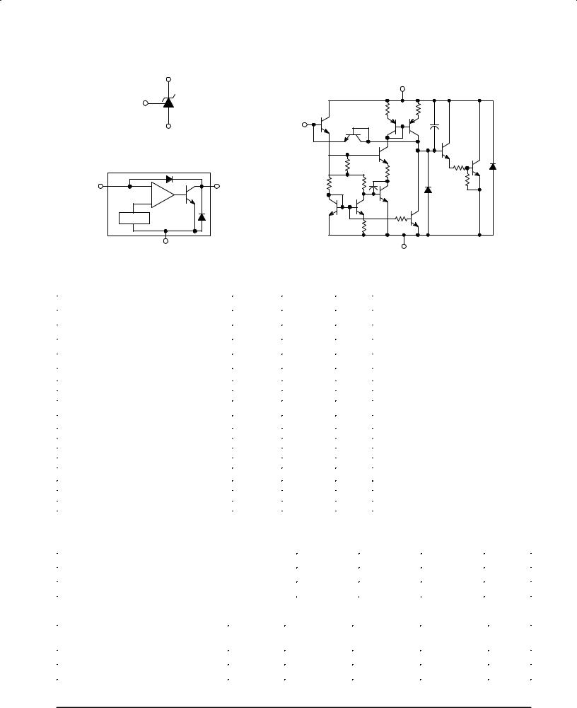
TL431, A, B Series
|
Symbol |
|
|
Cathode |
|
|
(K) |
|
|
Reference |
|
|
(R) |
|
|
Anode |
|
|
(A) |
|
Representative Block Diagram |
||
Reference |
|
Cathode |
(R) |
+ |
(K) |
|
± |
|
|
2.5 Vref |
|
|
Anode (A) |
|
Representative Schematic Diagram
Component values are nominal
Cathode (K)
Reference |
800 |
800 |
|
|
|
||
(R) |
|
20 pF |
|
|
3.28 k |
150 |
|
|
4.0 k |
||
|
20 pF |
||
|
10 k |
||
2.4 k |
7.2 k |
||
|
|||
|
|
1.0 k |
|
|
800 |
|
|
|
|
|
|
|
Anode (A) |
|
This device contains 12 active transistors. |
|||||
MAXIMUM RATINGS (Full operating ambient temperature range applies, unless |
|
|
||||
otherwise noted.) |
|
|
|
|
|
|
|
|
|
|
|
|
|
Rating |
|
Symbol |
Value |
|
Unit |
|
|
|
|
|
|
|
|
Cathode to Anode Voltage |
|
VKA |
37 |
|
V |
|
Cathode Current Range, Continuous |
|
IK |
±100 to +150 |
|
mA |
|
Reference Input Current Range, Continuous |
|
Iref |
±0.05 to +10 |
|
mA |
|
Operating Junction Temperature |
|
TJ |
150 |
|
°C |
|
Operating Ambient Temperature Range |
|
TA |
|
|
°C |
|
TL431I, TL431AI, TL431BI |
|
|
±40 to +85 |
|
|
|
TL431C, TL431AC, TL431BC |
|
|
0 to +70 |
|
|
|
|
|
|
|
|
|
|
Storage Temperature Range |
|
Tstg |
±65 to +150 |
|
°C |
|
Total Power Dissipation @ TA = 25°C |
|
PD |
|
|
W |
|
Derate above 25°C Ambient Temperature |
|
|
|
|
|
|
D, LP Suffix Plastic Package |
|
|
0.70 |
|
|
|
P Suffix Plastic Package |
|
|
1.10 |
|
|
|
DM Suffix Plastic Package |
|
|
0.52 |
|
|
|
|
|
|
|
|
|
|
Total Power Dissipation @ TC = 25°C |
|
PD |
|
|
W |
|
Derate above 25°C Case Temperature |
|
|
|
|
|
|
D, LP Suffix Plastic Package |
|
|
1.5 |
|
|
|
P Suffix Plastic Package |
|
|
3.0 |
|
|
|
|
|
|
|
|
|
|
NOTE: ESD data available upon request.
RECOMMENDED OPERATING CONDITIONS
Condition |
Symbol |
Min |
Max |
Unit |
|
|
|
|
|
Cathode to Anode Voltage |
VKA |
Vref |
36 |
V |
Cathode Current |
IK |
1.0 |
100 |
mA |
THERMAL CHARACTERISTICS
|
|
D, LP Suffix |
P Suffix |
DM Suffix |
|
Characteristic |
Symbol |
Package |
Package |
Package |
Unit |
|
|
|
|
|
|
Thermal Resistance, Junction±to±Ambient |
RθJA |
178 |
114 |
240 |
°C/W |
Thermal Resistance, Junction±to±Case |
RθJC |
83 |
41 |
± |
°C/W |
2 |
MOTOROLA ANALOG IC DEVICE DATA |

TL431, A, B Series
ELECTRICAL CHARACTERISTICS (TA = 25°C, unless otherwise noted.)
|
|
|
|
|
TL431I |
|
|
TL431C |
|
|
Characteristic |
Symbol |
|
|
|
|
|
|
|
||
Min |
Typ |
Max |
Min |
Typ |
Max |
Unit |
||||
|
|
|
|
|
|
|
|
|
|
|
Reference Input Voltage (Figure 1) |
|
Vref |
|
|
|
|
|
|
V |
|
VKA = Vref, IK = 10 mA |
|
|
|
|
|
|
|
|
|
|
TA = 25°C |
|
|
|
2.44 |
2.495 |
2.55 |
2.44 |
2.495 |
2.55 |
|
TA = Tlow to Thigh (Note 1) |
|
|
|
2.41 |
± |
2.58 |
2.423 |
± |
2.567 |
|
Reference Input Voltage Deviation Over |
|
Vref |
± |
7.0 |
30 |
± |
3.0 |
17 |
mV |
|
Temperature Range (Figure 1, Notes 1, 2) |
|
|
|
|
|
|
|
|
|
|
VKA= Vref, IK = 10 mA |
|
|
|
|
|
|
|
|
|
|
Ratio of Change in Reference Input Voltage |
|
DVref |
|
|
|
|
|
|
mV/V |
|
to Change in Cathode to Anode Voltage |
|
|
|
|
|
|
|
|
|
|
DVKA |
|
|
|
|
|
|
|
|||
IK = 10 mA (Figure 2), |
|
|
|
|
|
|
|
|||
VKA = 10 V to Vref |
|
|
|
± |
±1.4 |
±2.7 |
± |
±1.4 |
±2.7 |
|
VKA = 36 V to 10 V |
|
|
|
± |
±1.0 |
±2.0 |
± |
±1.0 |
±2.0 |
|
Reference Input Current (Figure 2) |
|
Iref |
|
|
|
|
|
|
μA |
|
IK = 10 mA, R1 = 10 k, R2 = ∞ |
|
|
|
|
|
|
|
|
|
|
TA = 25°C |
|
|
|
± |
1.8 |
4.0 |
± |
1.8 |
4.0 |
|
TA = Tlow to Thigh (Note 1) |
|
|
|
± |
± |
6.5 |
± |
± |
5.2 |
|
Reference Input Current Deviation Over |
|
Iref |
± |
0.8 |
2.5 |
± |
0.4 |
1.2 |
μA |
|
Temperature Range (Figure 2, Note 1, 4) |
|
|
|
|
|
|
|
|
|
|
IK = 10 mA, R1 = 10 k, R2 = ∞ |
|
|
|
|
|
|
|
|
|
|
Minimum Cathode Current For Regulation |
|
Imin |
± |
0.5 |
1.0 |
± |
0.5 |
1.0 |
mA |
|
VKA = Vref (Figure 1) |
|
|
|
|
|
|
|
|
|
|
Off±State Cathode Current (Figure 3) |
|
Ioff |
± |
260 |
1000 |
± |
260 |
1000 |
nA |
|
VKA = 36 V, Vref = 0 V |
|
|
|
|
|
|
|
|
|
|
Dynamic Impedance (Figure 1, Note 3) |
|
|ZKA| |
± |
0.22 |
0.5 |
± |
0.22 |
0.5 |
Ω |
|
VKA = Vref, IK = 1.0 mA to 100 mA |
|
|
|
|
|
|
|
|
|
|
f ≤ 1.0 kHz |
|
|
|
|
|
|
|
|
|
|
|
|
|
|
|
|
|
|
|
|
|
NOTES: 1. Tlow = ±40°C for TL431AIP TL431AILP, TL431IP, TL431ILP, TL431BID, TL431BIP, TL431BILP, TL431AIDM, TL431IDM, TL431BIDM |
|
= 0°C for TL431ACP, TL431ACLP, TL431CP, TL431CLP, TL431CD, TL431ACD, TL431BCD, TL431BCP, TL431BCLP, TL431CDM, |
|
TL431ACDM, TL431BCDM |
|
Thigh= +85°C for TL431AIP, TL431AILP, TL431IP, TL431ILP, TL431BID, TL431BIP, TL431BILP, TL431IDM, TL431AIDM, TL431BIDM |
|
= +70°C for TL431ACP, TL431ACLP, TL431CP, TL431ACD, TL431BCD, TL431BCP, TL431BCLP, TL431CDM, TL431ACDM, TL431BCDM |
|
2. The deviation parameter Vref is defined as the difference between the maximum and minimum values obtained over the full operating ambient |
|
temperature range that applies. |
|
Vref max |
Vref = Vref max |
|
±Vref min |
Vref min |
TA = T2 ± T1 |
|
|
|
|
|
T1 Ambient Temperature |
T2 |
|
|
|
||||||
The average temperature coefficient of the reference input voltage, αVref is defined as: |
|
|
|||||||||||
|
|
|
|
D Vref |
|
|
X 106 |
|
|
|
|
|
|
|
|
|
|
|
|
|
|
|
|
|
|
||
Vref |
ppm |
Vref @ 25_C |
+ |
|
D Vref x 106 |
||||||||
|
|
|
|||||||||||
_ |
+ |
|
D |
TA |
|
|
D |
TA |
(Vref |
_ |
|||
|
C |
|
|
|
|
|
@ 25 C) |
||||||
αVref can be positive or negative depending on whether Vref Min or Vref Max occurs at the lower ambient temperature. (Refer to Figure 6.)
Example : DVref + 8.0 mV and slope is positive, |
0.008 x 10⁶ |
||||
Vref @ 25_C + 2.495 V, DTA + 70_C |
|||||
a Vref + 70 (2.495) + 45.8 ppm _C |
|||||
3. The dynamic impedance ZKA is defined as |Z |
| + |
D VKA |
|
||
D IK |
|
|
|||
KA |
|
|
|||
When the device is programmed with two external resistors, R1 and R2, (refer to Figure 2) the total dynamic impedance of the circuit is defined as: |ZKA | [ |ZKA| 1 ) R1R2
MOTOROLA ANALOG IC DEVICE DATA |
3 |
|

TL431, A, B Series
ELECTRICAL CHARACTERISTICS (TA = 25°C, unless otherwise noted.)
|
|
|
|
|
TL431AI |
|
|
TL431AC |
|
|
TL431BI |
|
|
||||
Characteristic |
Symbol |
|
|
|
|
|
|
|
|
|
|
|
|
|
|
||
Min |
Typ |
|
Max |
Min |
|
Typ |
|
Max |
Min |
|
Typ |
Max |
Unit |
||||
|
|
|
|
|
|
|
|
|
|
|
|
|
|
|
|
|
|
Reference Input Voltage (Figure 1) |
|
Vref |
|
|
|
|
|
|
|
|
|
|
|
|
|
V |
|
VKA = Vref, IK = 10 mA |
|
|
|
|
|
|
|
|
|
|
|
|
|
|
|
|
|
TA = 25°C |
|
|
|
2.47 |
2.495 |
|
2.52 |
2.47 |
|
2.495 |
|
2.52 |
2.483 |
|
2.495 |
2.507 |
|
TA = Tlow to Thigh |
|
|
|
2.44 |
± |
|
2.55 |
2.453 |
|
± |
|
2.537 |
2.475 |
|
2.495 |
2.515 |
|
Reference Input Voltage Deviation Over |
|
Vref |
± |
7.0 |
|
30 |
± |
|
3.0 |
|
17 |
± |
|
3.0 |
17 |
mV |
|
Temperature Range (Figure 1, Notes 1, 2) |
|
|
|
|
|
|
|
|
|
|
|
|
|
|
|
|
|
VKA= Vref, IK = 10 mA |
|
|
|
|
|
|
|
|
|
|
|
|
|
|
|
|
|
Ratio of Change in Reference Input Voltage |
|
DVref |
|
|
|
|
|
|
|
|
|
|
|
|
|
mV/V |
|
to Change in Cathode to Anode Voltage |
|
|
|
|
|
|
|
|
|
|
|
|
|
|
|
|
|
DVKA |
|
|
|
|
|
|
|
|
|
|
|
|
|
|
|||
IK = 10 mA (Figure 2), |
|
|
|
|
|
|
|
|
|
|
|
|
|
|
|||
VKA = 10 V to Vref |
|
|
|
± |
±1.4 |
|
±2.7 |
± |
|
±1.4 |
|
±2.7 |
± |
|
±1.4 |
±2.7 |
|
VKA = 36 V to 10 V |
|
|
|
± |
±1.0 |
|
±2.0 |
± |
|
±1.0 |
|
±2.0 |
± |
|
±1.0 |
±2.0 |
|
Reference Input Current (Figure 2) |
|
Iref |
|
|
|
|
|
|
|
|
|
|
|
|
|
μA |
|
IK = 10 mA, R1 = 10 k, R2 = ∞ |
|
|
|
|
|
|
|
|
|
|
|
|
|
|
|
|
|
TA = 25°C |
|
|
|
± |
1.8 |
|
4.0 |
± |
|
1.8 |
|
4.0 |
± |
|
1.1 |
2.0 |
|
TA = Tlow to Thigh (Note 1) |
|
|
|
± |
± |
|
6.5 |
± |
|
± |
|
5.2 |
± |
|
± |
4.0 |
|
Reference Input Current Deviation Over |
|
Iref |
± |
0.8 |
|
2.5 |
± |
|
0.4 |
|
1.2 |
± |
|
0.8 |
2.5 |
μA |
|
Temperature Range (Figure 2, Note 1) |
|
|
|
|
|
|
|
|
|
|
|
|
|
|
|
|
|
IK = 10 mA, R1 = 10 k, R2 = ∞ |
|
|
|
|
|
|
|
|
|
|
|
|
|
|
|
|
|
Minimum Cathode Current For Regulation |
|
Imin |
± |
0.5 |
|
1.0 |
± |
|
0.5 |
|
1.0 |
± |
|
0.5 |
1.0 |
mA |
|
VKA = Vref (Figure 1) |
|
|
|
|
|
|
|
|
|
|
|
|
|
|
|
|
|
Off±State Cathode Current (Figure 3) |
|
Ioff |
± |
260 |
|
1000 |
± |
|
260 |
|
1000 |
± |
|
230 |
500 |
nA |
|
VKA = 36 V, Vref = 0 V |
|
|
|
|
|
|
|
|
|
|
|
|
|
|
|
|
|
Dynamic Impedance (Figure 1, Note 3) |
|
|ZKA| |
± |
0.22 |
|
0.5 |
± |
|
0.22 |
|
0.5 |
± |
|
0.14 |
0.3 |
Ω |
|
VKA = Vref, IK = 1.0 mA to 100 mA |
|
|
|
|
|
|
|
|
|
|
|
|
|
|
|
|
|
f ≤ 1.0 kHz |
|
|
|
|
|
|
|
|
|
|
|
|
|
|
|
|
|
|
|
|
|
|
|
|
|
|
|
|
|
|
|
|
|
|
|
NOTES: 1. Tlow = ±40°C for TL431AIP TL431AILP, TL431IP, TL431ILP, TL431BID, TL431BIP, TL431BILP, TL431AIDM, TL431IDM, TL431BIDM |
|
= 0°C for TL431ACP, TL431ACLP, TL431CP, TL431CLP, TL431CD, TL431ACD, TL431BCD, TL431BCP, TL431BCLP, TL431CDM, |
|
TL431ACDM, TL431BCDM |
|
Thigh= +85°C for TL431AIP, TL431AILP, TL431IP, TL431ILP, TL431BID, TL431BIP, TL431BILP, TL431IDM, TL431AIDM, TL431BIDM |
|
= +70°C for TL431ACP, TL431ACLP, TL431CP, TL431ACD, TL431BCD, TL431BCP, TL431BCLP, TL431CDM, TL431ACDM, TL431BCDM |
|
2. The deviation parameter Vref is defined as the difference between the maximum and minimum values obtained over the full operating ambient |
|
temperature range that applies. |
|
Vref max |
Vref = Vref max |
|
±Vref min |
Vref min |
TA = T2 ± T1 |
|
|
|
|
|
T1 Ambient Temperature |
T2 |
|
|
|
||||||
The average temperature coefficient of the reference input voltage, αVref is defined as: |
|
|
|||||||||||
|
|
|
|
D Vref |
|
|
X 106 |
|
|
|
|
|
|
|
|
|
|
|
|
|
|
|
|
|
|
||
Vref |
ppm |
Vref @ 25_C |
+ |
|
D Vref x 106 |
||||||||
|
|
|
|||||||||||
_ |
+ |
|
D |
TA |
|
|
D |
TA |
(Vref |
_ |
|||
|
C |
|
|
|
|
|
@ 25 C) |
||||||
αVref can be positive or negative depending on whether Vref Min or Vref Max occurs at the lower ambient temperature. (Refer to Figure 6.)
Example : DVref + 8.0 mV and slope is positive, |
0.008 x 10⁶ |
||||
Vref @ 25_C + 2.495 V, DTA + 70_C |
|||||
a Vref + 70 (2.495) + 45.8 ppm _C |
|||||
3. The dynamic impedance ZKA is defined as |Z |
| + |
D VKA |
|
||
KA |
|
D IK |
|
|
|
When the device is programmed with two external resistors, R1 and R2, (refer to Figure 2) the total dynamic impedance of the circuit is defined as: |ZKA | [ |ZKA| 1 ) R1R2
4 |
MOTOROLA ANALOG IC DEVICE DATA |

TL431, A, B Series
Figure 1. Test Circuit for VKA = Vref |
Figure 2. Test Circuit for VKA > Vref |
Figure 3. Test Circuit for Ioff |
Input |
Input |
|
VKA |
|
|
|
IK |
|
|
R1 |
Iref |
Vref |
R2 |
|
|
|
Vref |
Figure 4. Cathode Current versus
Cathode Voltage
|
150 |
|
|
|
|
|
|
|
VKA = Vref |
|
|
|
|
(mA) |
100 |
TA = 25°C |
|
|
|
|
Input |
VKA |
|
|
|
||
CURRENT |
|
IK |
|
|
|
|
50 |
|
|
|
|
|
|
|
|
|
|
|
|
|
, CATHODE |
0 |
|
|
|
|
|
±50 |
|
|
|
|
|
|
K |
|
|
|
|
|
|
I |
|
|
|
|
|
|
|
±100 |
±1.0 |
0 |
1.0 |
2.0 |
3.0 |
|
±2.0 |
|||||
VKA, CATHODE VOLTAGE (V)
VKA |
Input |
V |
|
|
KA |
IK |
|
Ioff |
|
|
|
VKA + Vref 1 ) R2R1 |
) Iref S R1 |
|
|
|
|
Figure 5. Cathode Current versus |
|||
|
800 |
|
|
Cathode Voltage |
|
|
|
|
|
|
|
|
|
|
|
|
VKA = Vref |
|
|
|
μA) |
600 |
Input |
TA = 25°C |
|
IMin |
|
|
VKA |
|
||||
( |
|
|
|
IK |
|
|
CURRENT |
400 |
|
|
|
|
|
CATHODE, |
200 |
|
|
|
|
|
|
|
|
|
|
|
|
K |
0 |
|
|
|
|
|
I |
|
|
|
|
|
|
|
±200 |
|
0 |
1.0 |
2.0 |
3. |
|
±1.0 |
|||||
|
|
|
|
VKA, CATHODE VOLTAGE (V) |
|
|
Figure 6. Reference Input Voltage versus
Ambient Temperature
|
2600 |
|
VKA |
|
|
|
|
|
(mV) |
Input |
|
|
|
|
|
||
2580 |
|
IKV |
= V |
|
|
|
|
|
VOLTAGE |
|
|
KA |
ref |
|
Vref Max = 2550 mV |
|
|
2560 |
V |
IK = 10 mA |
|
|
||||
|
ref |
|
|
|
|
|
|
|
2540 |
|
|
|
|
|
|
|
|
2520 |
|
|
|
|
|
|
|
|
INPUT |
|
|
|
|
|
|
|
|
2500 |
|
|
|
|
Vref Typ = 2495 mV |
|
||
, REFERENCE |
2480 |
|
|
|
|
|
|
|
2460 |
|
|
|
|
|
|
|
|
2440 |
|
|
|
|
Vref Min = 2440 mV |
|||
2420 |
|
|
|
|
|
|
|
|
ref |
|
|
|
|
|
|
|
|
|
|
|
|
|
|
|
|
|
V |
2400 |
±25 |
0 |
25 |
50 |
75 |
100 |
125 |
|
||||||||
|
±55 |
|||||||
|
|
|
TA, AMBIENT TEMPERATURE (°C) |
|
|
|||
Figure 7. Reference Input Current versus Ambient Temperature
( μA) |
3.0 |
|
|
|
|
|
|
|
|
|
|
|
|
|
|
|
|
|
|
CURRENT |
2.5 |
|
|
|
|
|
|
|
|
2.0 |
|
|
|
|
|
|
|
|
|
|
|
|
|
|
|
|
|
|
|
INPUT |
1.5 |
|
|
|
|
|
|
|
|
|
|
|
|
|
|
|
|
|
|
REFERENCE |
1.0 |
Input |
IK = 10 mA |
VKA |
|
|
|
|
|
Iref |
IK |
|
|
|
|
||||
|
10k |
|
|
|
|
|
|||
0.5 |
|
|
|
|
|
|
|
|
|
, |
|
|
|
|
|
|
|
|
|
ref |
|
|
|
|
|
|
|
|
|
I |
0 |
|
|
|
|
|
|
|
|
|
±25 |
0 |
25 |
50 |
75 |
100 |
12 |
||
|
±55 |
||||||||
|
|
|
TA, AMBIENT TEMPERATURE (°C) |
|
|
||||
MOTOROLA ANALOG IC DEVICE DATA |
5 |
|
 Loading...