

MOTOROLA MC14076BD, MC14076BDR2, MC14076BCP Datasheet
MC14076B
4-Bit D-Type Register
with Three-State Outputs
The MC14076B 4–Bit Register consists of four D–type flip–flops
operating synchronously from a common clock. OR gated
output–disable inputs force the outputs into a high–impedance state
for use in bus organized systems. OR gated data–disable inputs cause
the Q outputs to be fed back to the D inputs of the flip–flops. Thus they
are inhibited from changing state while the clocking process remains
undisturbed. An asynchronous master root is provided to clear all four
flip–flops simultaneously independent of the clock or disable inputs.
• Three–State Outputs with Gated Control Lines
• Fully Independent Clock Allows Unrestricted Operation for the T wo
Modes: Parallel Load and Do Nothing
• Asynchronous Master Reset
• Four Bus Buffer Registers
• Supply Voltage Range = 3.0 Vdc to 18 Vdc
• Capable of Driving T wo Low–Power TTL Loads or One Low–Power
Schottky TTL Load Over the Rated T emperature Range
MAXIMUM RATINGS (Voltages Referenced to V
Symbol Parameter Value Unit
V
DD
Vin, V
Iin, I
P
T
T
stg
T
1. Maximum Ratings are those values beyond which damage to the device
may occur.
2. Temperature Derating:
Plastic “P and D/DW” Packages: – 7.0 mW/_C From 65_C To 125_C
DC Supply Voltage Range –0.5 to +18.0 V
Input or Output Voltage Range
out
out
D
A
L
(DC or Transient)
Input or Output Current
(DC or Transient) per Pin
Power Dissipation,
per Package (Note 2.)
Ambient Temperature Range –55 to +125 °C
Storage Temperature Range –65 to +150 °C
Lead Temperature
(8–Second Soldering)
) (Note 1.)
SS
–0.5 to VDD + 0.5 V
±10 mA
500 mW
260 °C
http://onsemi.com
MARKING
DIAGRAMS
16
PDIP–16
P SUFFIX
CASE 648
SOIC–16
D SUFFIX
CASE 751B
A = Assembly Location
WL or L = Wafer Lot
YY or Y = Year
WW or W = Work Week
MC14076BCP
AWLYYWW
1
16
14076B
AWLYWW
1
ORDERING INFORMATION
Device Package Shipping
MC14076BCP PDIP–16 2000/Box
MC14076BD SOIC–16 2400/Box
MC14076BDR2 SOIC–16 2500/Tape & Reel
This device contains protection circuitry to guard against damage due to high
static voltages or electric fields. However, precautions must be taken to avoid
applications of any voltage higher than maximum rated voltages to this
high–impedance circuit. For proper operation, V
to the range V
Unused inputs must always be tied to an appropriate logic voltage level (e.g.,
either V
SS
Semiconductor Components Industries, LLC, 2000
March, 2000 – Rev . 3
v (Vin or V
SS
or VDD). Unused outputs must be left open.
) v VDD.
out
and V
in
should be constrained
out
1 Publication Order Number:
MC14076B/D
MC14076B
Data
Output
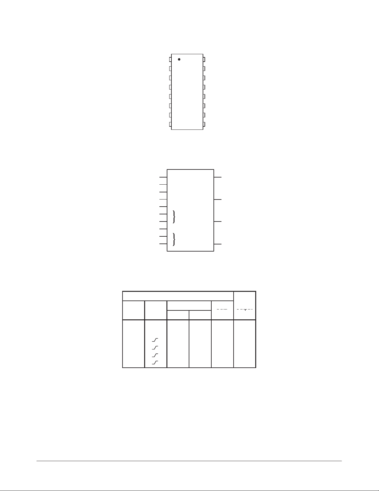
PIN ASSIGNMENT
OUTPUT
DISABLE
15
14
13
12
11
10
1
A
{
2
B
Q0
3
4
Q1
Q2
Q3
6
7
C
8
V
SS
BLOCK DIAGRAM
RESET
D0
D1
D2
D3
DATA
B
DISABLE
A
9
7
CLOCK
OUTPUT
B
2
1
A
DISABLE
V
16
DD
R
15
D0
14
D1
13
D2
125
11
D3
10
B
DATA
}
DISABLE
9
A
Q0
3
4
Q1
5
Q2
Q3
6
= PIN 16
V
DD
V
= PIN 8
SS
FUNCTION TABLE
Inputs
Data Disable
Reset Clock
1 X X X X 0
0 0 X X X Q
0 1 X X Q
0 X 1 X Q
0 0 0 0 0
0 0 0 1 1
When either output disable A or B (or both) is (are) high the
output is disabled to the high–impedance state; however
sequential operation of the flip–flops is not affected.
X = Don’t Care.
A B
Data Output
D
Q
n
n
n
http://onsemi.com
2
MC14076B
V
DD
Î
Î
Î
Î
Î
Î
Î
Î
Î
Î
Î
Î
Î
Î
Î
Î
Î
Î
Î
Î
Î
Î
Î
Î
Î
Î
Î
Î
Î
Î
Î
Î
Î
Î
Î
Î
Î
Î
Î
Î
Î
Î
Î
Î
Î
Î
Î
Î
Î
Î
Î
Î
Î
Î
Î
Î
Î
Î
Î
Î
Î
Î
Î
Î
Î
Î
Î
Î
Î
Î
Î
Î
Î
Î
Î
Î
Î
Î
Î
Î
Î
Î
Î
Î
Î
Î
Î
Î
Î
Î
Î
Î
Î
Î
Î
Î
Î
Î
Î
Î
Î
Î
Î
Î
Î
Î
Î
Î
Î
Î
Î
Î
Î
Î
Î
Î
Î
Î
Î
Î
Î
Î
Î
Î
Î
Î
Î
Î
Î
Î
Î
Î
Î
Î
Î
Î
Î
Î
Î
Î
Î
Î
Î
Î
Î
Î
Î
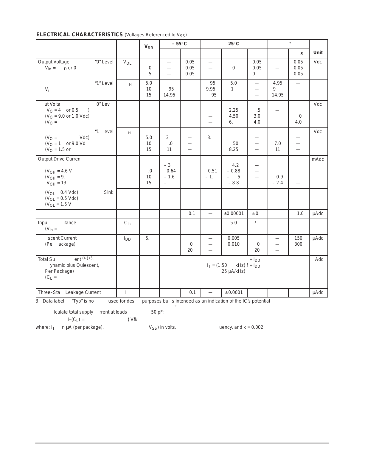
ELECTRICAL CHARACTERISTICS (Voltages Referenced to V
V
Characteristic
Output Voltage “0” Level
= VDD or 0
V
in
ОООООООО
“1” Level
V
= 0 or V
ОООООООО
in
Input Voltage “0” Level
ОООООООО
(V
O
(V
ОООООООО
O
(V
O
ОООООООО
(V
O
(V
O
ОООООООО
(V
O
Output Drive Current
ОООООООО
(V
OH
(V
ОООООООО
OH
(V
OH
ОООООООО
(V
OH
DD
= 4.5 or 0.5 Vdc)
= 9.0 or 1.0 Vdc)
= 13.5 or 1.5 Vdc)
“1” Level
= 0.5 or 4.5 Vdc)
= 1.0 or 9.0 Vdc)
= 1.5 or 13.5 Vdc)
= 2.5 Vdc) Source
= 4.6 Vdc)
= 9.5 Vdc)
= 13.5 Vdc)
(VOL = 0.4 Vdc) Sink
(V
= 0.5 Vdc)
OL
ОООООООО
(V
= 1.5 Vdc)
OL
Input Current
Input Capacitance
ОООООООО
(V
= 0)
in
Quiescent Current
(Per Package)
ОООООООО
Total Supply Current
ОООООООО
(Dynamic plus Quiescent,
Per Package)
ОООООООО
= 50 pF on all outputs, all
(C
L
ОООООООО
buffers switching)
(4.) (5.)
Three–State Leakage Current
Symbol
V
OL
ÎÎ
V
OH
ÎÎ
V
ÎÎ
ÎÎ
V
ÎÎ
ÎÎ
I
OH
ÎÎ
ÎÎ
ÎÎ
I
OL
ÎÎ
I
in
C
ÎÎ
I
DD
ÎÎ
I
ÎÎ
ÎÎ
ÎÎ
I
TL
Vdc
5.0
10
Î
15
5.0
10
Î
15
IL
Î
5.0
10
Î
15
IH
Î
5.0
10
Î
15
Î
5.0
5.0
Î
10
Î
15
5.0
10
Î
15
15
in
—
Î
5.0
10
Î
15
T
5.0
Î
10
15
Î
Î
15
Min
—
—
Î
—
4.95
9.95
Î
14.95
Î
—
—
Î
—
Î
3.5
7.0
Î
11
Î
– 3.0
– 0.64
Î
– 1.6
Î
– 4.2
0.64
1.6
Î
4.2
—
—
Î
—
—
Î
—
ООООООООООООООО
ООООООООООООООО
ООООООООООООООО
—
SS
– 55_C
)
Max
0.05
0.05
Î
0.05
—
—
Î
—
Î
1.5
3.0
Î
4.0
Î
—
—
Î
—
Î
—
—
Î
—
Î
—
—
—
Î
—
± 0.1
—
Î
5.0
10
Î
20
± 0.1
25_C
Min
—
—
ÎÎ
—
4.95
9.95
ÎÎ
14.95
ÎÎ
—
—
ÎÎ
—
ÎÎ
3.5
7.0
ÎÎ
11
ÎÎ
– 2.4
– 0.51
ÎÎ
– 1.3
ÎÎ
– 3.4
0.51
1.3
ÎÎ
3.4
—
—
ÎÎ
—
—
ÎÎ
—
(3.)
Typ
0
0
Î
0
5.0
10
Î
15
Î
2.25
4.50
Î
6.75
Î
2.75
5.50
Î
8.25
Î
– 4.2
– 0.88
Î
– 2.25
Î
– 8.8
0.88
2.25
Î
8.8
±0.00001
5.0
Î
0.005
0.010
Î
0.015
IT = (0.75 µA/kHz) f + I
IT = (1.50 µA/kHz) f + I
IT = (2.25 µA/kHz) f + I
—
± 0.0001
Max
0.05
0.05
ÎÎ
0.05
—
—
ÎÎ
—
ÎÎ
1.5
3.0
ÎÎ
4.0
ÎÎ
—
—
ÎÎ
—
ÎÎ
—
—
ÎÎ
—
ÎÎ
—
—
—
ÎÎ
—
± 0.1
7.5
ÎÎ
5.0
10
ÎÎ
20
DD
DD
DD
± 0.1
Min
—
—
Î
—
4.95
9.95
Î
14.95
Î
—
—
Î
—
Î
3.5
7.0
Î
11
Î
– 1.7
– 0.36
Î
– 0.9
Î
– 2.4
0.36
0.9
Î
2.4
—
—
Î
—
—
Î
—
—
125_C
Max
0.05
0.05
Î
0.05
Î
Î
Î
Î
Î
Î
Î
Î
Î
± 1.0
Î
Î
± 3.0
3. Data labelled “Typ” is not to be used for design purposes but is intended as an indication of the IC’s potential performance.
4. The formulas given are for the typical characteristics only at 25_C.
5. To calculate total supply current at loads other than 50 pF:
I
) = IT(50 pF) + (CL – 50) Vfk
T(CL
where: I
is in µA (per package), CL in pF, V = (VDD – VSS) in volts, f in kHz is input frequency, and k = 0.002.
T
—
—
—
1.5
3.0
4.0
—
—
—
—
—
—
—
—
—
—
—
150
300
600
Unit
Vdc
Î
Vdc
Î
Vdc
Î
Î
Vdc
Î
Î
mAdc
Î
Î
Î
mAdc
Î
µAdc
pF
Î
µAdc
Î
µAdc
Î
Î
Î
µAdc
http://onsemi.com
3
 Loading...