


M38C37MCMXXXFS
Table of contents
 Loading...
Mitsubishi M38C37MCMXXXFS, M38C37MCMXXXFP, M38C37MCAXXXFS, M38C37MBMXXXFS, M38C37MBMXXXFP Datasheet
...
38C3 Group
PIN CONFIGURATION (TOP VIEW)
Package type : 80P6N-A
80-pin plastic-molded QFP
DESCRIPTION
The 38C3 group is the 8-bit microcomputer based on the 740 family
core technology.
The 38C3 group has a LCD drive control circuit, a 10-channel A-D
converter, and a Serial I/O as additional functions.
The various microcomputers in the 38C3 group include variations of
internal memory size and packaging. For details, refer to the section
on part numbering.
For details on availability of microcomputers in the 38C3 group, refer
to the section on group expansion.
FEATURES
●Basic machine-language instructions ....................................... 71
●The minimum instruction execution time............................. 0.5 µs
(at 8MHz oscillation frequency)
●Memory size
ROM ..................................................................4 K to 48 K bytes
RAM ................................................................. 192 to 1024 bytes
●Programmable input/output ports ............................................. 57
●Software pull-up/pull-down resistors
..................................................... (Ports P0–P8 except Port P5
1)
●Interrupts................................................... 16 sources, 16 vectors
(includes key input interrupt)
●Timers ............................................................8-bit ✕ 6, 16-bit ✕ 1
●A-D converter.................................................10-bit ✕ 8 channels
●Serial I/O ....................................... 8-bit ✕ 1 (Clock-synchronized)
●LCD drive control circuit
Bias ............................................................................ 1/1, 1/2, 1/3
Duty .................................................................... 1/1, 1/2, 1/3, 1/4
Common output .......................................................................... 4
Segment output ........................................................................ 32
●2 Clock generating circuit
(connect to external ceramic resonator or quartz-crystal oscillator)
●Power source voltage
In high-speed mode ....................................................4.0 to 5.5 V
In middle-speed mode ................................................2.5 to 5.5 V
In low-speed mode...................................................... 2.5 to 5.5 V
●Power dissipation
In high-speed mode ...........................................................32 mW
(at 8 MHz oscillation frequency)
In low-speed mode..............................................................45 µW
(at 32 kHz oscillation frequency , at 3 V power source voltage)
●Operating temperature range.................................... – 20 to 85°C
APPLICATIONS
Camera, household appliances, consumer electronics, etc.
MITSUBISHI MICROCOMPUTERS
SINGLE-CHIP 8-BIT CMOS MICROCOMPUTER
Fig. 1 M38C34M6AXXXFP pin configuration
1
25
26
27
28
29
30
31
32
33
34
35
36
37
38
39
40
64
65
66
67
68
69
70
71
72
73
74
75
76
77
78
79
80
P64/AN4
P65/AN5
P66/AN6
P67/AN7
AV
SS
VREF
P60/AN0
P61/AN1
P62/AN2
P63/AN3
VCC
VSS
XOUT
P70/XcIN
P71/XcOUT
XIN
RESET
VL1
COM3
COM2
COM1
COM0
VL3
VL2
P40/SCLK2
P42/T3OUT
P43/φ
P44/SIN
P45/SOUT
P46/SCLK1
P47/SRDY
P41/T1OUT
P80
P81
P82
P83
P84
P85
P86
P87
P30/SEG24
P33/SEG27
P34/SEG28
P35/SEG29
P36/SEG30
P37/SEG31
P31/SEG25
P32/SEG26
M38C34M6AXXXFP
P51
P52/PWM1
P53/CNTR0
P54/CNTR1
P55/INT0
P56/INT1
P57/INT2
P50/TAOUT
P10/SEG16
P11/SEG17
P12/SEG18
P13/SEG19
P14/SEG20
P15/SEG21
P16/SEG22
P17/SEG23
P00/SEG8
P01/SEG9
P02/SEG10
P03/SEG11
P04/SEG12
P05/SEG13
P06/SEG14
P07/SEG15
P27/SEG7
P26/SEG6
P25/SEG5
P24/SEG4
P23/SEG3
P22/SEG2
P21/SEG1
P20/SEG0
63
62
61
60
59
58
57
56
55
54
53
52
51
50
49
48
47
46
45
44
43
42
41
2
3
4
5
6
7
8
9
10
11
12
13
14
15
16
17
18
19
20
21
22
23
24
2
SINGLE-CHIP 8-BIT CMOS MICROCOMPUTER
MITSUBISHI MICROCOMPUTERS
38C3 Group
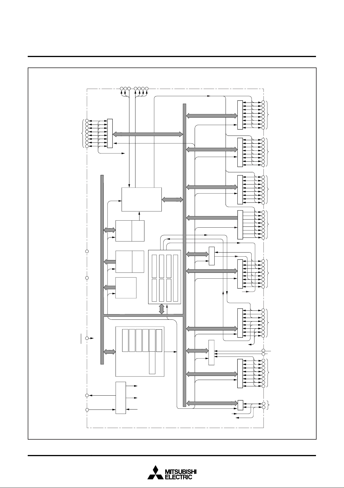
FUNCTIONAL BLOCK DIAGRAM
Fig. 2 Functional block diagram
Key-on wake-up
INT
0
–INT
2
CNTR
0
,CNTR
1
T1
OUT,
T3
OUT
φ
Data bus
C P U
A
X
Y
S
PC
H
PC
L
PS
RESET
V
CC
V
SS
Reset input ( 5 V ) ( 0 V )
R O M
R A M
LCD display
RAM
(16 bytes)
10 16
13
I/O port P5
P4(8)
I/O port P4
I/O port P2
P2(8)
I/O port P1
P1(8)
P6(8)
Output port P3
I/O port P6
P5(8)
I/O port P7
P7(2)
28
27
26
32
31
30
29
I/O port P0
P0(8)
49
50 51
52 53 54
55
5641 42 43 44 45
46 47
48
57
58
59
60
61
62 63
6467 68 69 70 71 7265
66
12
11
1
2
75 76
77
78
79
80 7374
456789
17
3
Clock generating
circuit
Main
clock
input
X
IN
Main
clock
output
X
OUT
X
COUT
Sub-
clock
output
X
CIN
Sub-
clock
input
SI/O(8)
V
REF
AV
SS
( 0 V )
A-D converter(10)
Timer 1(8) Timer 2(8)
LCD
drive control
circuit
V
L1
V
L2
V
L3
COM
0
COM
1
COM
2
COM
3
φ
X
CIN
X
COUT
14
15
Timer 3(8) Timer 4(8)
Timer 5(8) Timer 6(8)
P3(8)
33 34
35
36
37
38 39
40
R O M
corrective
circuit
ROM corrective
RAM
(8 bytes)
I/O port P8
P8(8)
18 19 20 21 22 23 24 25
PWM
0,
PWM
1
Timer A(16)
3
SINGLE-CHIP 8-BIT CMOS MICROCOMPUTER
MITSUBISHI MICROCOMPUTERS
38C3 Group
• Apply voltage of 2.5 V to 5.5 V to VCC, and 0 V to VSS.
• Reference voltage input pin for A-D converter .
• GND input pin for A-D converter.
• Connect to VSS.
• Reset input pin for active “L.”
• Input and output pins for the main clock generating circuit.
• Feedback resistor is built in between XIN pin and XOUT pin.
• Connect a ceramic resonator or a quartz-crystal oscillator between the XIN and XOUT pins to set the
oscillation frequency.
• If an external clock is used, connect the clock source to the XIN pin and leave the XOUT pin open.
• Input 0 ≤ VL1 ≤ VL2 ≤ VL3 ≤ VCC voltage.
• Input 0 – VL3 voltage to LCD.
• LCD common output pins.
• COM1, COM2, and COM3 are not used at 1/1 duty ratio.
• COM2 and COM3 are not used at 1/2 duty ratio.
• COM3 is not used at 1/3 duty ratio.
• 8-bit I/O port.
• CMOS compatible input level.
• CMOS 3-state output structure.
• I/O direction register allows each port to be individually
programmed as either input or output.
• Pull-down control is enabled.
• 8-bit output port.
• CMOS state output.
• Pull-down control is enabled.
• 8-bit I/O port.
• CMOS compatible input level.
• CMOS 3-state output structure.
• I/O direction register allows each pin to be individually
programmed as either input or output.
• Pull-up control is enabled.
• LCD segment pins
• Serial I/O function pin
• Timer output pin
• Timer output pin
• φ output pin
• Serial I/O function pins
Pin
V
CC, VSS
VREF
AVSS
RESET
XIN
XOUT
VL1 – VL3
COM0 –
COM3
P00/SEG9 –
P07/SEG15
P10/SEG16 –
P17/SEG23
P20/SEG0 –
P27/SEG7
P30/SEG24 –
P37/SEG31
P40/SCLK2
P41/T1OUT
P42/T3OUT
P43/φ
P44/SIN,
P45/SOUT,
P46/SCLK1,
P47/SRDY
Name
Power source
Analog reference
voltage
Analog power
source
Reset input
Clock input
Clock output
LCD power
source
Common output
I/O port P0
I/O port P1
I/O port P2
Output port P3
I/O port P4
Function except a port function
PIN DESCRIPTION
Table 1 Pin description (1)
Function
4
SINGLE-CHIP 8-BIT CMOS MICROCOMPUTER
MITSUBISHI MICROCOMPUTERS
38C3 Group
• 1-bit input pin.
• CMOS compatible input level.
• 7-bit I/O port.
• CMOS compatible input level.
• CMOS 3-state output structure.
• I/O direction register allows each pin to be individually
programmed as either input or output.
• Pull-up control is enabled.
• 8-bit I/O port.
• CMOS compatible input level.
• CMOS 3-state output structure.
• I/O direction register allows each pin to be individually
programmed as either input or output.
• Pull-up control is enabled.
• 2-bit I/O port.
• CMOS compatible input level.
• CMOS 3-state output structure.
• I/O direction register allows each pin to be individually
programmed as either input or output.
• Pull-up control is enabled.
• 8-bit I/O port.
• TTL input level.
• CMOS 3-state output structure.
• I/O direction register allows each pin to be individually
programmed as either input or output.
• Pull-up control is enabled.
Pin
P51
P50/TAOUT
P52/PWM1
P53/CNTR0,
P54/CNTR1
P55/INT0,
P56/INT1,
P57/INT2
P60/AN0 –
P67/AN7
P70/XCOUT,
P71/XCIN
P80 – P87
Table 2 Pin description (2)
Name
Input port P5
I/O port P5
I/O port P6
I/O port P7
I/O port P8
Function except a port function
• Timer A output pin
• PWM1 output (timer output) pin
• External count I/O pins
• External interrupt input pins
• A-D conversion input pins
• Sub-clock generating circuit I/O pins
• Key input (Key-on wake-up) interrupt
input pins
Function
5
SINGLE-CHIP 8-BIT CMOS MICROCOMPUTER
MITSUBISHI MICROCOMPUTERS
38C3 Group
M38C3 4 M 6 A XXX
FPProduct
ROM/PROM size
1
2
3
4
5
6
7
8
: 4096 bytes
: 8192 bytes
: 12288 bytes
: 16384 bytes
: 20480 bytes
: 24576 bytes
: 28672 bytes
: 32768 bytes
The first 128 bytes and the last 2 bytes of ROM
are reserved areas ; they cannot be used.
Memory type
M
E
: Mask ROM version
: EPROM or One Time PROM version
RAM size
0
1
2
3
4
5
6
7
: 192 bytes
: 256 bytes
: 384 bytes
: 512 bytes
: 640 bytes
: 768 bytes
: 896 bytes
: 1024 bytes
Package type
FP
FS
ROM number
Omitted in some types.
A : Standard(Note)
M : M version
: 80P6N-A package
: 80D0 package
9
A
B
C
: 36864 bytes
: 40960 bytes
: 45056 bytes
: 49152 bytes
Note : Difference between standard and M version
• Standard :
• M version :
Port P5
0
/TA
OUT
pin remains set to the input mode until the direction
register is set to the output mode during reset and after
reset.
Port P5
0
/TA
OUT
pin remains set to the output mode (“L” output) until
the direction register is set to the input mode during reset
and after reset.
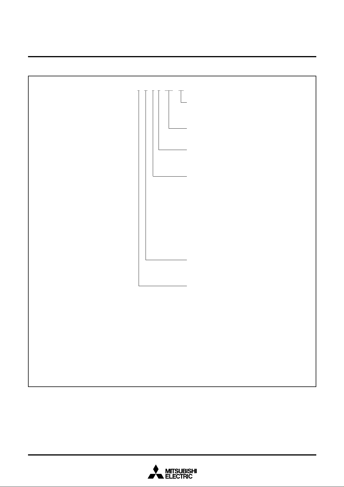
P ART NUMBERING
Fig. 3 Part numbering
6
SINGLE-CHIP 8-BIT CMOS MICROCOMPUTER
MITSUBISHI MICROCOMPUTERS
38C3 Group
ROM size (bytes)
32K
28K
24K
20K
16K
12K
8K
4K
256 384 512 640 768 896
1024
192
RAM size (bytes)
36K
40K
44K
48K
Under development
M38C34M6A/M6M
Under development
M38C37ECA/ECM
Planning
M38C33M4
Products under development or planning : the development schedule and specification may be revised without notice.
Planning products may be stopped the development.
GROUP EXPANSION
Mitsubishi plans to expand the 38C3 group as follows.
Memory T ype
Support for mask ROM, One Time PROM, and EPROM versions
Memory Size
ROM/PROM size ................................................ 16 K to 48 K bytes
RAM size............................................................. 512 to 1024 bytes
Memory Expansion Plan
Fig. 4 Memory expansion plan
Currently planning products are listed below.
As of April 1998
Package
80P6N-A
80D0
80P6N-A
80D0
Product name
M38C34M6AXXXFP
M38C37ECAXXXFP
M38C37ECAFP
M38C37ECAFS
M38C34M6MXXXFP
M38C37ECMXXXFP
M38C37ECMFP
M38C37ECMFS
(P) ROM size (bytes)
ROM size for User in ( )
24576 (24446)
49152 (49022)
24576 (24446)
49152 (49022)
RAM size
(bytes)
640
1024
640
1024
Table 3 Support products
Mask ROM version
One Time PROM version
One Time PROM version (blank)
EPROM version
Mask ROM version
One Time PROM version
One Time PROM version (blank)
EPROM version
Remarks
Packages
80P6N-A ..................................... 0.8 mm-pitch plastic molded QFP
80D0 ........................ 0.8 mm-pitch ceramic LCC (EPROM version)
7
SINGLE-CHIP 8-BIT CMOS MICROCOMPUTER
MITSUBISHI MICROCOMPUTERS
38C3 Group
Not available
Processor mode bits
b1 b0
0 0 : Single-chip mode
0 1 :
1 0 :
1 1 :
Stack page selection bit
0 : RAM in the zero page is used as stack area
1 : RAM in page 1 is used as stack area
Not used (returns “1” when read)
(Do not write “0” to this bit.)
Port X
C
switch bit
0 : I/O port
1 : X
CIN
, X
COUT
Main clock ( X
IN
–X
OUT
) stop bit
0 : Operating
1 : Stopped
Main clock division ratio selection bit
0 : f(X
IN
)/2 (high-speed mode)
1 : f(X
IN
)/8 (middle-speed mode)
Internal system clock selection bit
0 : X
IN
-X
OUT
selected (middle-/high-speed mode)
1 : X
CIN
-X
COUT
selected (low-speed mode)
CPU mode register
(CPUM (CM) : address 003B
16
)
b7 b0
FUNCTIONAL DESCRIPTION
CENTRAL PROCESSING UNIT (CPU)
The 38C3 group uses the standard 740 family instruction set. Refer
to the table of 740 family addressing modes and machine instruc-
tions or the 740 Family Software Manual for details on the instruction
set.
Machine-resident 740 family instructions are as follows:
The FST and SLW instruction cannot be used.
The STP, WIT, MUL, and DIV instruction can be used.
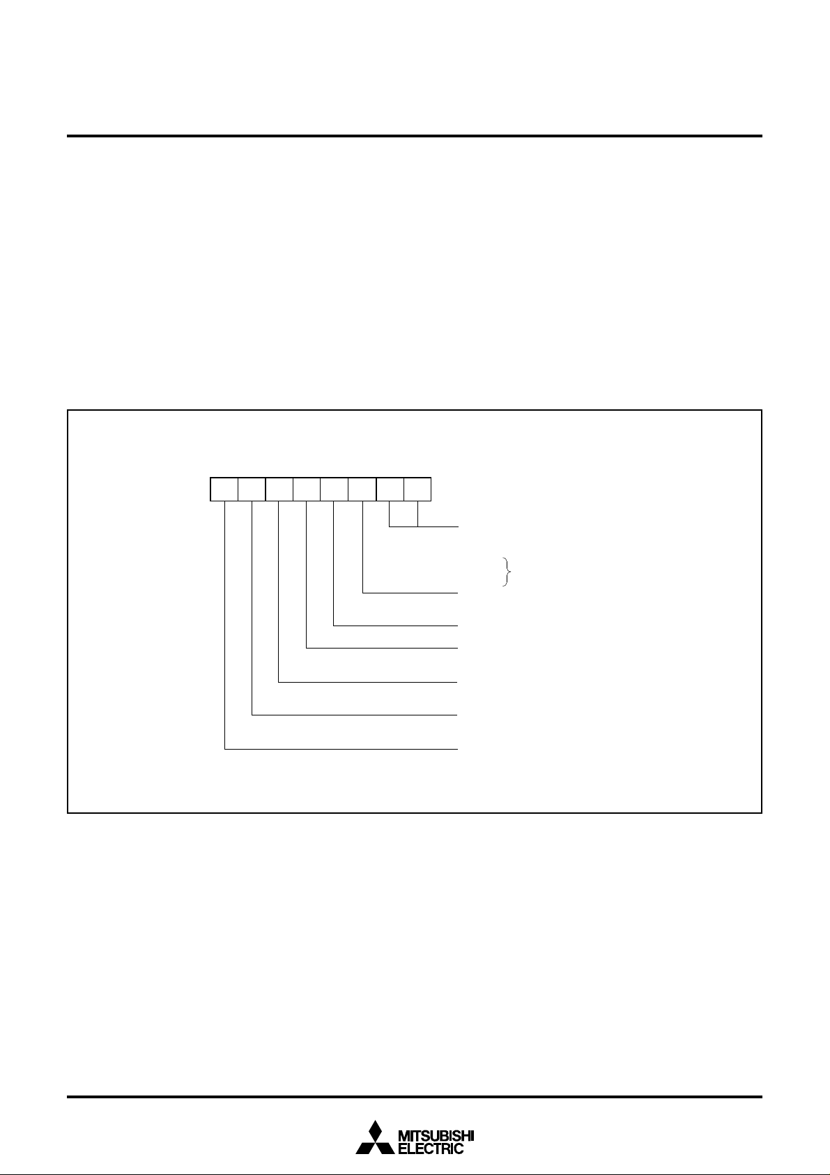
[CPU Mode Register (CPUM)] 003B16
The CPU mode register contains the stack page selection bit and the
internal system clock selection bit.
The CPU mode register is allocated at address 003B
16.
Fig. 5 Structure of CPU mode register
8
SINGLE-CHIP 8-BIT CMOS MICROCOMPUTER
MITSUBISHI MICROCOMPUTERS
38C3 Group
192
256
384
512
640
768
896
1024
00FF
16
013F
16
01BF
16
023F
16
02BF
16
033F
16
03BF
16
043F
16
RAM area
RAM size
(bytes)
Address
XXXX
16
4096
8192
12288
16384
20480
24576
28672
32768
36864
40960
45056
49152
F000
16
E000
16
D000
16
C000
16
B000
16
A000
16
9000
16
8000
16
7000
16
6000
16
5000
16
4000
16
F080
16
E080
16
D080
16
C080
16
B080
16
A080
16
9080
16
8080
16
7080
16
6080
16
5080
16
4080
16
ROM area
ROM size
(bytes)
Address
YYYY
16
Address
ZZZZ
16
0058
16
0000
16
0040
16
0440
16
FF00
16
FFDC
16
FFFE
16
FFFF
16
XXXX
16
YYYY
16
ZZZZ
16
RAM
ROM
0050
16
Reserved area
SFR area 1
Not used
Interrupt vector area
Reserved ROM area
(128 bytes)
Zero page
Special page
LCD display RAM area
Reserved ROM area
ROM corrective RAM area
0100
16
(Note 1)
SFR area 2 (Note 1)
0F00
16
0FFF
16
Note 1 : This is valid only in mask ROM version.
MEMORY
Special Function Register (SFR) Area
The Special Function Register area in the zero page contains control
registers such as I/O ports and timers.
RAM
RAM is used for data storage and for stack area of subroutine calls
and interrupts.
ROM
The first 128 bytes and the last 2 bytes of ROM are reserved for
device testing and the rest is user area for storing programs.
Interrupt Vector Area
The interrupt vector area contains reset and interrupt vectors.
Zero Page
Access to this area with only 2 bytes is possible in the zero page
addressing mode.
Special Page
Access to this area with only 2 bytes is possible in the special page
addressing mode.
Fig. 6 Memory map diagram

9
SINGLE-CHIP 8-BIT CMOS MICROCOMPUTER
MITSUBISHI MICROCOMPUTERS
38C3 Group
Fig. 7 Memory map of special function register (SFR)
ROM correct high-order address register 1 (Note)
ROM correct high-order address register 2 (Note)
ROM correct high-order address register 3 (Note)
ROM correct high-order address register 4 (Note)
Port P8 output selection register (P8SEL)
0020
16
0021
16
0022
16
0023
16
0024
16
0025
16
0026
16
0027
16
0028
16
0029
16
002A
16
002B
16
002C
16
002D
16
002E
16
002F
16
0030
16
0031
16
0032
16
0033
16
0034
16
0035
16
0036
16
0037
16
0038
16
0039
16
003A
16
003B
16
003C
16
003D
16
003E
16
003F
16
0000
16
0001
16
0002
16
0003
16
0004
16
0005
16
0006
16
0007
16
0008
16
0009
16
000A
16
000B
16
000C
16
000D
16
000E
16
000F
16
0010
16
0011
16
0012
16
0013
16
0014
16
0015
16
0016
16
0017
16
0018
16
0019
16
001A
16
001B
16
001C
16
001D
16
001E
16
001F
16
Port P0 (P0)
Port P0 direction register (P0D)
Port P1 (P1)
Port P1 direction register (P1D)
Port P2 (P2)
Port P2 direction register (P2D)
Port P3 (P3)
Port P4 (P4)
Port P4 direction register (P4D)
Port P5 (P5)
Port P5 direction register (P5D)
Port P6 (P6)
Port P6 direction register (P6D)
Port P7 (P7)
Port P7 direction register (P7D)
Serial I/O control register 1 (SIOCON1)
Serial I/O control register 2 (SIOCON2)
Serial I/O register (SIO)
Interrupt control register 2 (ICON2)
Timer 6 PWM register (T6PWM)
Interrupt edge selection register (INTEDGE)
CPU mode register (CPUM)
Interrupt request register 1 (IREQ1)
Interrupt request register 2 (IREQ2)
Interrupt control register 1 (ICON1)
Timer 1 (T1)
Timer 3 (T3)
Timer 5 (T5)
Timer 6 (T6)
Timer 2 (T2)
Timer 4 (T4)
PULL register A (PULLA)
PULL register B (PULLB)
Timer 12 mode register (T12M)
Timer 34 mode register (T34M)
Timer 56 mode register (T56M)
Segment output enable register (SEG)
LCD mode register (LM)
A-D control register (ADCON)
A-D conversion register (low) (ADL)
Port P8 (P8)
Port P8 direction register (P8D)
φ output control register (CKOUT)
Timer A register (low) (TAL)
Timer A register (high) (TAH)
Compare register (low) (CONAL)
Compare register (high) (CONAH)
Timer A mode register (TAM)
Timer A control register (TACON)
A-D conversion register (high) (ADH)
0F0A
16
0F0B
16
0F0C
16
0F0D
16
0F0E
16
0F0F
16
0F10
16
0F11
16
ROM correct enable register 1 (Note)
ROM correct low-order address register 1 (Note)
ROM correct high-order address register 5 (Note)
ROM correct low-order address register 5 (Note)
ROM correct high-order address register 6 (Note)
ROM correct low-order address register 6 (Note)
ROM correct high-order address register 7 (Note)
ROM correct low-order address register 7 (Note)
ROM correct high-order address register 8 (Note)
ROM correct low-order address register 8 (Note)
0F01
16
0F02
16
0F03
16
0F07
16
0F08
16
0F09
16
0F04
16
0F05
16
0F06
16
ROM correct low-order address register 2 (Note)
ROM correct low-order address register 3 (Note)
ROM correct low-order address register 4 (Note)
Note: This register is valid only in mask ROM version.
10
SINGLE-CHIP 8-BIT CMOS MICROCOMPUTER
MITSUBISHI MICROCOMPUTERS
38C3 Group
I/O PORTS
[Direction Registers (ports P2, P4, P5
0, P52–P57,
and P6–P8)]
The I/O ports P2, P4, P50, P52–P57, and P6–P8 have direction reg-
isters which determine the input/output direction of each individual
pin. Each bit in a direction register corresponds to one pin, each pin
can be set to be input port or output port.
When “0” is written to the bit corresponding to a pin, that pin be-
comes an input pin. When “1” is written to that bit, that pin becomes
an output pin.
If data is read from a pin set to output, the value of the port output
latch is read, not the value of the pin itself. Pins set to input are float-
ing. If a pin set to input is written to, only the port output latch is
written to and the pin remains floating.
[Direction Registers (ports P0 and P1)]
Ports P0 and P1 have direction registers which determine the input/
output direction of each individual port.
Each port in a direction register corresponds to one port, each port
can be set to be input or output.
When “0” is written to the bit 0 of a direction register, that port be-
comes an input port. When “1” is written to that port, that port be-
comes an output port. Bits 1 to 7 of ports P0 and P1 direction regis-
ters are not used.
Pull-up/Pull-down Control
By setting the PULL register A (address 001616) or the PULL register
B (address 0017
16), ports except for ports P3 and P51 can control
either pull-down or pull-up (pins that are shared with the segment
output pins for LCD are pull-down; all other pins are pull-up) with a
program.
However, the contents of PULL register A and PULL register B do
not affect ports programmed as the output ports.
Port P8 Output Selection
Ports P80 to P87 can be switched to N-channel open-drain output by
setting “1” to the port P8 output selection register.
Fig. 8 Structure of PULL register A and PULL register B
Pin
P00/SEG8 –
P07/SEG15
P10/SEG16 –
P17/SEG23
P20/SEG0 –
P27/SEG7
P30/SEG24 –
P37/SEG31
Name
Port P0
Port P1
Port P2
Port P3
Input/Output
Input/Output,
port unit
Input/Output,
port unit
Input/Output,
individual bits
Output,
individual bits
I/O format
CMOS compatible input
level
CMOS 3-state output
CMOS compatible input
level
CMOS 3-state output
CMOS compatible input
CMOS 3-state output
CMOS 3-state output
Non-port function
LCD segment output
LCD segment output
LCD segment output
LCD segment output
Related SFRs
PULL register A
Segment output enable reg-
ister
PULL register A
Segment output enable reg-
ister
PULL register A
Segment output enable reg-
ister
Segment output enable reg-
ister
Ref. No.
(1)
(2)
Table 4 List of I/O port function (1)
Fig. 9 Structure of port P8 output selection register
P0
0
–P0
7
pull-down
P1
0
–P1
7
pull-down
P2
0
–P2
7
pull-down
Not used
P7
0
, P7
1
pull-up
P8
0
–P8
7
pull-up
PULL register A
(PULLA : address 0016
16
)
b7 b0
P4
0
–P4
3
pull-up
P4
4
–P4
7
pull-up
P5
0
, P5
2
, P5
3
pull-up
P5
4
–P5
7
pull-up
P6
0
, P6
3
pull-up
P6
4
–P6
7
pull-up
Not used (return “0” when read)
0 : Disable
1 : Enable
PULL register B
(PULLB : address 0017
16
)
b7 b0
Note : The contents of PULL register A and PULL register B
do not affect ports programmed as the output ports.
Not used (return “0” when read)
0 : CMOS output (in output mode)
1 : N-channel open-drain output
(in output mode)
Port P8 output selection register
(P8SEL : address 0018
16)
b7 b0
11
SINGLE-CHIP 8-BIT CMOS MICROCOMPUTER
MITSUBISHI MICROCOMPUTERS
38C3 Group
Pin
P40/SCLK2
P41/T1OUT
P42/T3OUT
P43/φ
P44/SIN
P45/SOUT
P46/SCLK1
P47/SRDY
P50/TAOUT
P51
P52/PWM1
P53/CNTR0
P54/CNTR1
P55/INT0
P56/INT1
P57/INT2
P60/AN0
–
P67/AN7
P70/XCIN
P71/XCOUT
P80 – P87
COM
0
– COM
3
Name
Port P4
Port P5
Port P6
Port P7
Port P8
Common
Input/Output
Input/Output,
individual bits
Input/Output,
individual bits
Input
Input/Output,
individual bits
Input/Output,
individual bits
Input/Output,
individual bits
Input/Output,
individual bits
Output
I/O format
CMOS compatible input
level
CMOS 3-state output
CMOS compatible input
level
CMOS 3-state output
CMOS compatible input
level
CMOS compatible input
level
CMOS 3-state output
CMOS compatible input
level
CMOS 3-state output
CMOS compatible input
level
CMOS 3-state output
CMOS compatible input
level
CMOS 3-state output
LCD common output
Non-port function
Serial I/O function I/O
Timer output
Timer output
φ clock output
Serial I/O function I/O
Timer A output
PWM output
External count I/O
External interrupt in-
put
A-D converter input
Sub-clock generating
circuit I/O
Key input (key-on
wake-up) interrupt in-
put
Related SFRs
Serial I/O control registers
1, 2
PULL register B
Timer 12 mode register
PULL register B
Timer 34 mode register
PULL register B
φ output control register
PULL register B
Serial I/O control registers
1, 2
PULL register B
Timer A mode register
Timer A control reigster
PULL register B
Timer 56 mode register
PULL register B
Interrupt edge selection reg-
ister
PULL register B
Interrupt edge selection reg-
ister
PULL register B
A-D control register
PULL register B
CPU mode register
PULL register A
Interrupt control register 2
PULL register A
LCD mode register
Ref. No.
(3)
(4)
(4)
(5)
(6)
(7)
(8)
(9)
(10)
(11)
(4)
(12)
(12)
(13)
(14)
(15)
(17)
(16)
Table 5 List of I/O port function (2)
Notes 1: Make sure that the input level at each pin is either 0 V or VCC during execution of the STP instruction.
When an input level is at an intermediate potential, a current will flow from V
CC to VSS through the input-stage gate.
2: For details of the functions of ports P0 to P3 in modes other than single-chip mode, and how to use double function ports as function I/O ports, refer to the
applicable sections.
12
SINGLE-CHIP 8-BIT CMOS MICROCOMPUTER
MITSUBISHI MICROCOMPUTERS
38C3 Group
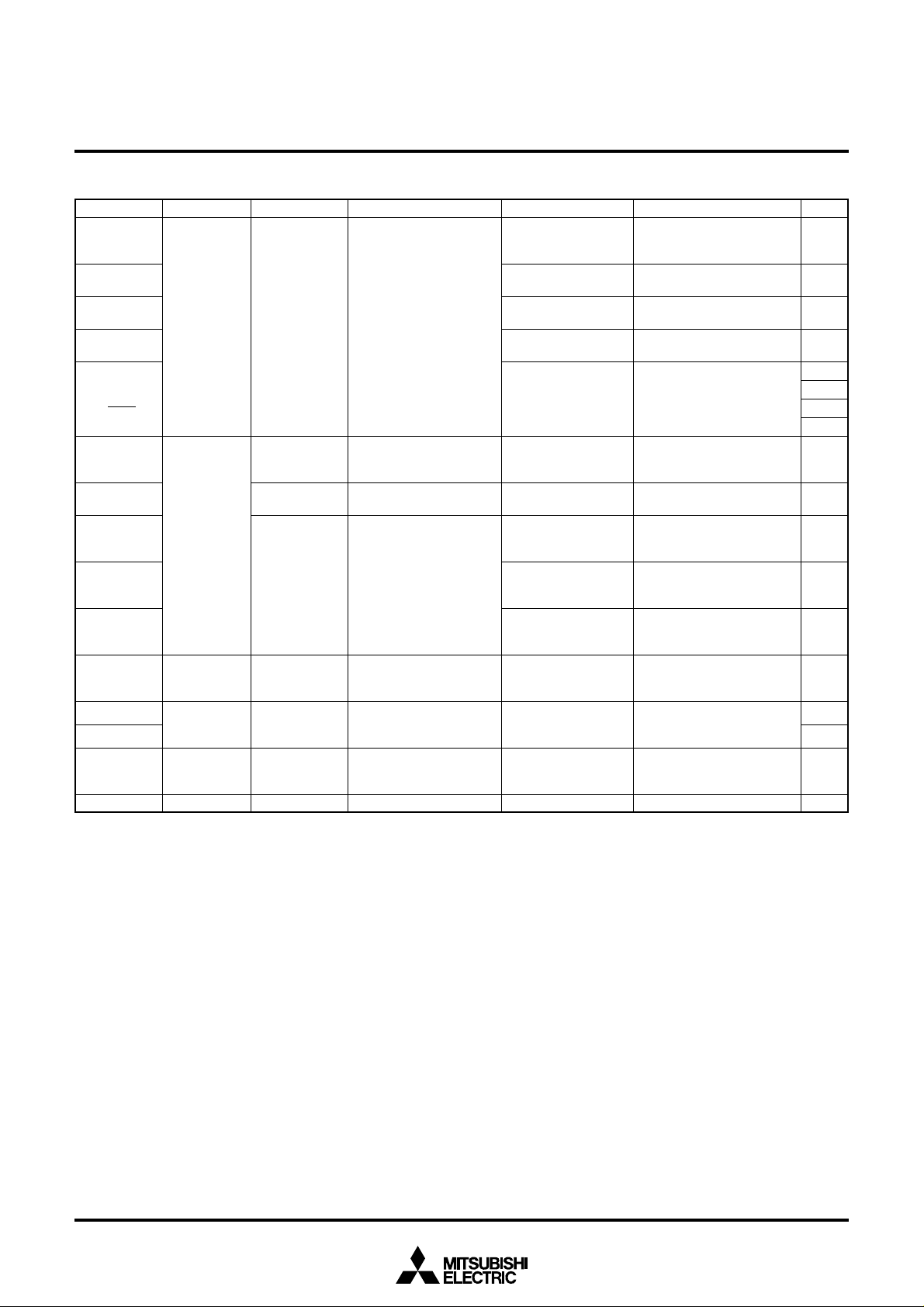
Fig. 10 Port block diagram (1)
(6)Port P4
4
Serial I/O input
(1)Ports P0, P1, P2
Segment output enable bit
Pull-down control
Segment output enable bit
Direction register
Data bus
Port latch
V
L2
/V
L3
V
L1
/V
SS
(5)Port P4
3
φ
φ output control bit
(2)Port P3
Segment output enable bit
Pull-down control
Segment output enable bit
Data bus Port latch
V
L2
/V
L3
V
L1
/V
SS
(4)Ports P4
1
, P4
2
, P5
2
Timer 1 output selection bit
Timer 3 output selection bit
Timer 6 output selection bit
Direction register
Pull-up control
Timer 1 output
Timer 3 output
Timer 6 output
(3)Port P4
0
Data bus
Serial I/O clock output
Serial I/O mode selection bit
Port latch
Direction register
Pull-up control
P-channel output disable bit
(Note)
Note : Port P0, P1 direction registers are only bit 0.
Data bus
Port latch
Port latch
Direction register
Data bus
Pull-up control
Data bus
Port latch
Direction register
Pull-up control
13
SINGLE-CHIP 8-BIT CMOS MICROCOMPUTER
MITSUBISHI MICROCOMPUTERS
38C3 Group
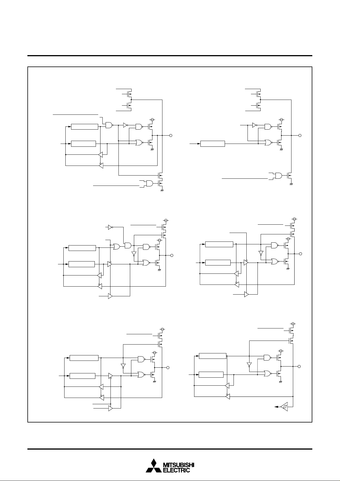
Fig. 11 Port block diagram (2)
(7)Port P4
5
Data bus
Serial I/O port selection bit
Serial I/O output
P-channel output disable bit
Port latch
Direction register
Pull-up control
(9)Port P4
7
Data bus
Serial I/O ready output
Port latch
S
RDY
output enable bit
Direction register
Pull-up control
(8)Port P4
6
Serial I/O clock output
Serial I/O clock input
Serial I/O mode selection bit
Port latch
Direction register
Pull-up control
P-channel output disable bit
(10)Port P5
0
Data bus
Port latch
Direction register
Pull-up control
Timer A output enable bit
Timer A output
(12)Ports P5
3
–P5
7
INT
0
–INT
2
interrupt input
Data bus
Direction register
Port latch
Pull-up control
(11)Port P5
1
Data bus
(Note)
Note: The initihal value of M version becomes “1” (output).
Data bus
CNTR
0
,CNTR
1
interrupt input
14
SINGLE-CHIP 8-BIT CMOS MICROCOMPUTER
MITSUBISHI MICROCOMPUTERS
38C3 Group
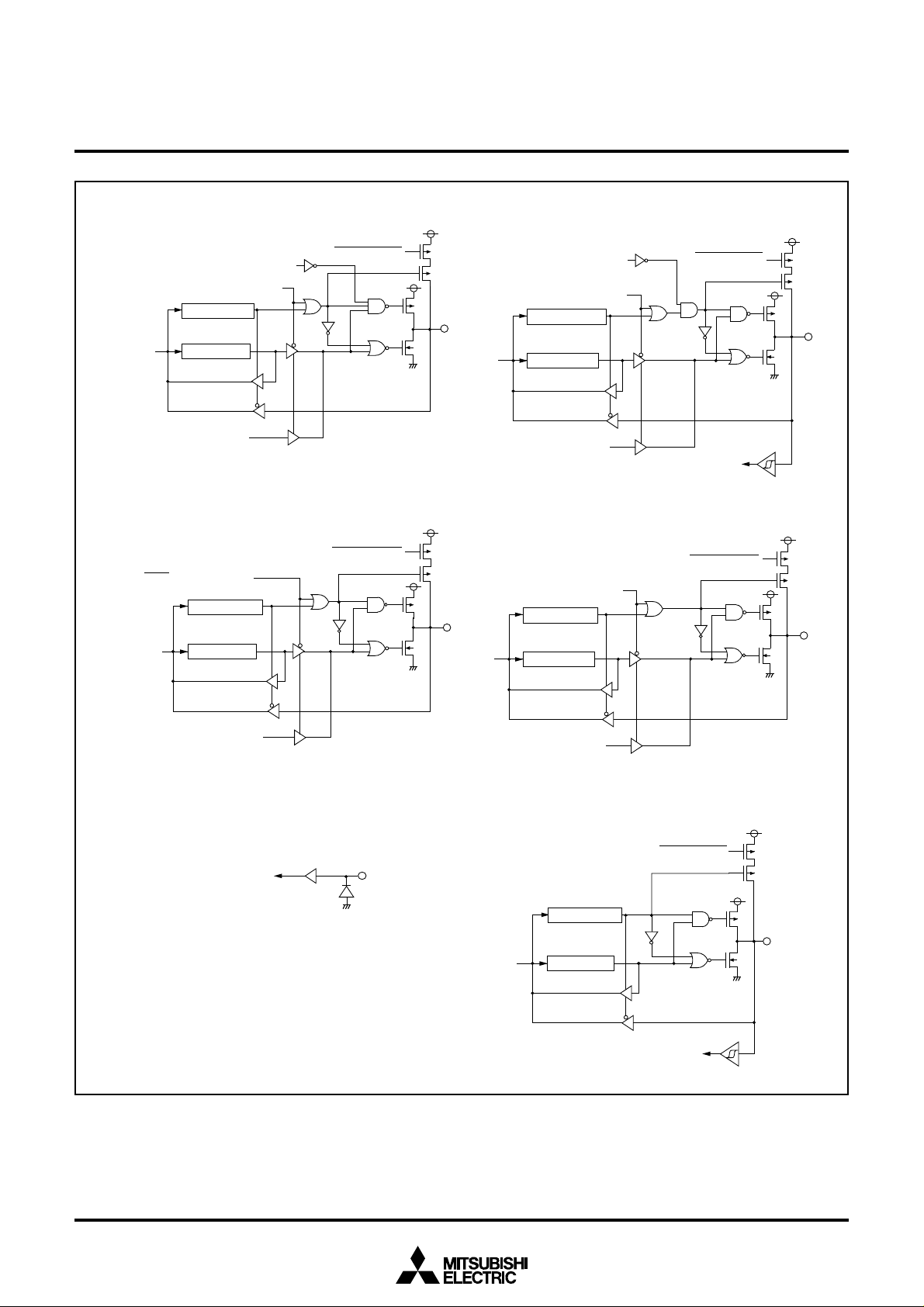
Fig. 12 Port block diagram (3)
(14)Port P7
0
Direction register
Data bus
Port latch
Port selection • pull-up control
Oscillator
Port P7
0
(15)Port P7
1
Direction register
Data bus
Port Xc switch bit
Port latch
Port selection • pull-up control
Sub-clock generating circuit input
(16)COM
0
–COM
3
V
L3
V
L2
V
L1
The gate input signal of each
transistor is controlled by the
LCD duty ratio and the bias
value.
(13)Port P6
Analog input pin selection bit
A-D conversion input
Data bus
Port latch
Direction register
Pull-up control
(17)Port P8
Key input (key-on wake-up) interrupt input
Data bus
Direction register
Port latch
Pull-up control
P-channel output disable bit
Port Xc switch bit
Port Xc switch bit

15
SINGLE-CHIP 8-BIT CMOS MICROCOMPUTER
MITSUBISHI MICROCOMPUTERS
38C3 Group
INTERRUPTS
Interrupts occur by sixteen sources: six external, nine internal, and
one software.
Interrupt Control
Each interrupt except the BRK instruction interrupt have both an in-
terrupt request bit and an interrupt enable bit, and is controlled by the
interrupt disable flag. An interrupt occurs if the corresponding inter-
rupt request and enable bits are “1” and the interrupt disable flag is
“0”.
Interrupt enable bits can be set or cleared by software. Interrupt re-
quest bits can be cleared by software, but cannot be set by software.
The BRK instruction interrupt and reset cannot be disabled with any
flag or bit. The I flag disables all interrupts except the BRK instruction
interrupt and reset. If several interrupts requests occurs at the same
time the interrupt with highest priority is accepted first.
Interrupt Operation
By acceptance of an interrupt, the following operations are automati-
cally performed:
1.The processing being executed is stopped.
2.The contents of the program counter and processor status reg-
ister are automatically pushed onto the stack.
3.The interrupt disable flag is set and the corresponding interrupt
request bit is cleared.
4.The interrupt jump destination address is read from the vector
table into the program counter.
■Notes on Interrupts
When the active edge of an external interrupt (INT
0 – INT2, CNTR0
or CNTR1) is set or an vector interrupt source where several interrupt
source is assigned to the same vector address is switched, the cor-
responding interrupt request bit may also be set. Therefore, take fol-
lowing sequence:
(1) Disable the interrupt.
(2) Change the active edge in interrupt edge selection register.
(3) Clear the set interrupt request bit to “0.”
(4) Enable the interrupt.
16
SINGLE-CHIP 8-BIT CMOS MICROCOMPUTER
MITSUBISHI MICROCOMPUTERS
38C3 Group
Interrupt Source
Reset (Note 2)
INT0
INT1
INT2
Serial I/O
Timer A
Timer 1
Timer 2
Timer 3
Timer 4
Timer 5
Timer 6
CNTR0
CNTR1
Key input (Key-
on wake-up)
A-D conversion
BRK instruction
Priority
1
2
3
4
5
6
7
8
9
10
11
12
13
14
15
16
17
Vector Addresses (Note 1)
High
FFFD16
FFFB16
FFF916
FFF716
FFF516
FFF316
FFF116
FFEF16
FFED16
FFEB16
FFE916
FFE716
FFE516
FFE316
FFE116
FFDF16
FFDD16
Interrupt Request
Generating Conditions
At reset
At detection of either rising or falling edge of
INT
0 intput
At detection of either rising or falling edge of
INT1 input
At detection of either rising or falling edge of
INT2 input
At completion of serial I/O data transmit/re-
ceive
At timer A underflow
At timer 1 underflow
At timer 2 underflow
At timer 3 underflow
At timer 4 underflow
At timer 5 underflow
At timer 6 underflow
At detection of either rising or falling edge of
CNTR0 input
At detection of either rising or falling edge of
CNTR1 input
At falling of port P8 (at input) input logical level
AND
At completion of A-D conversion
At BRK instruction execution
Remarks
Non-maskable
External interrupt
(active edge selectable)
External interrupt
(active edge selectable)
External interrupt
(active edge selectable)
Valid when serial I/O is selected
STP release timer underflow
External interrupt
(active edge selectable)
External interrupt
(active edge selectable)
External interrupt
(falling valid)
Valid when A-D conversion interrupt
is selected
Non-maskable software interrupt
Low
FFFC16
FFFA16
FFF816
FFF616
FFF416
FFF216
FFF016
FFEE16
FFEC16
FFEA16
FFE816
FFE616
FFE416
FFE216
FFE016
FFDE16
FFDC16
Notes 1: Vector addresses contain interrupt jump destination addresses.
2: Reset function in the same way as an interrupt with the highest priority.
Table 6 Interrupt vector addresses and priority

17
SINGLE-CHIP 8-BIT CMOS MICROCOMPUTER
MITSUBISHI MICROCOMPUTERS
38C3 Group
b7 b0
Interrupt edge selection register
INT
0
interrupt edge selection bit
INT
1
interrupt edge selection bit
INT
2
interrupt edge selection bit
Not used (return “0” when read)
CNTR
0
active edge switch bit
CNTR
1
active edge switch bit
(INTEDGE : address 003A
16
)
Interrupt request register 1
INT
0
interrupt request bit
INT
1
interrupt request bit
INT
2
interrupt request bit
Serial I/O interrupt request bit
Timer A interrupt request bit
Timer 1 interrupt request bit
Timer 2 interrupt request bit
Timer 3 interrupt request bit
Interrupt control register 1
INT
0
interrupt enable bit
INT
1
interrupt enable bit
INT
2
interrupt enable bit
Serial I/O interrupt enable bit
Timer A interrupt enable bit
Timer 1 interrupt enable bit
Timer 2 interrupt enable bit
Timer 3 interrupt enable bit
0 : No interrupt request issued
1 : Interrupt request issued
(IREQ1 : address 003C
16
)
(ICON1 : address 003E
16
)
Interrupt request register 2
Timer 4 interrupt request bit
Timer 5 interrupt request bit
Timer 6 interrupt request bit
CNTR
0
interrupt request bit
CNTR
1
interrupt request bit
Key input interrupt request bit
AD conversion interrupt request bit
Not used (returns “0” when read)
(IREQ2 : address 003D
16
)
Interrupt control register 2
Timer 4 interrupt enable bit
Timer 5 interrupt enable bit
Timer 6 interrupt enable bit
CNTR
0
interrupt enable bit
CNTR
1
interrupt enable bit
Key input interrupt enable bit
AD conversion interrupt enable bit
Not used (returns “0” when read)
(Do not write “1” to this bit)
0 : Interrupts disabled
1 : Interrupts enabled
(ICON2 : address 003F
16
)
0 : Falling edge active
1 : Rising edge active
b7 b0
b7 b0
b7 b0
b7 b0
0 : Falling edge active, rising edge count
1 : Rising edge active, falling edge count
Interrupt request bit
Interrupt enable bit
Interrupt disable flag (I)
BRK instruction
Reset
Interrupt request
Fig. 13 Interrupt control
Fig. 14 Structure of interrupt-related registers
18
SINGLE-CHIP 8-BIT CMOS MICROCOMPUTER
MITSUBISHI MICROCOMPUTERS
38C3 Group
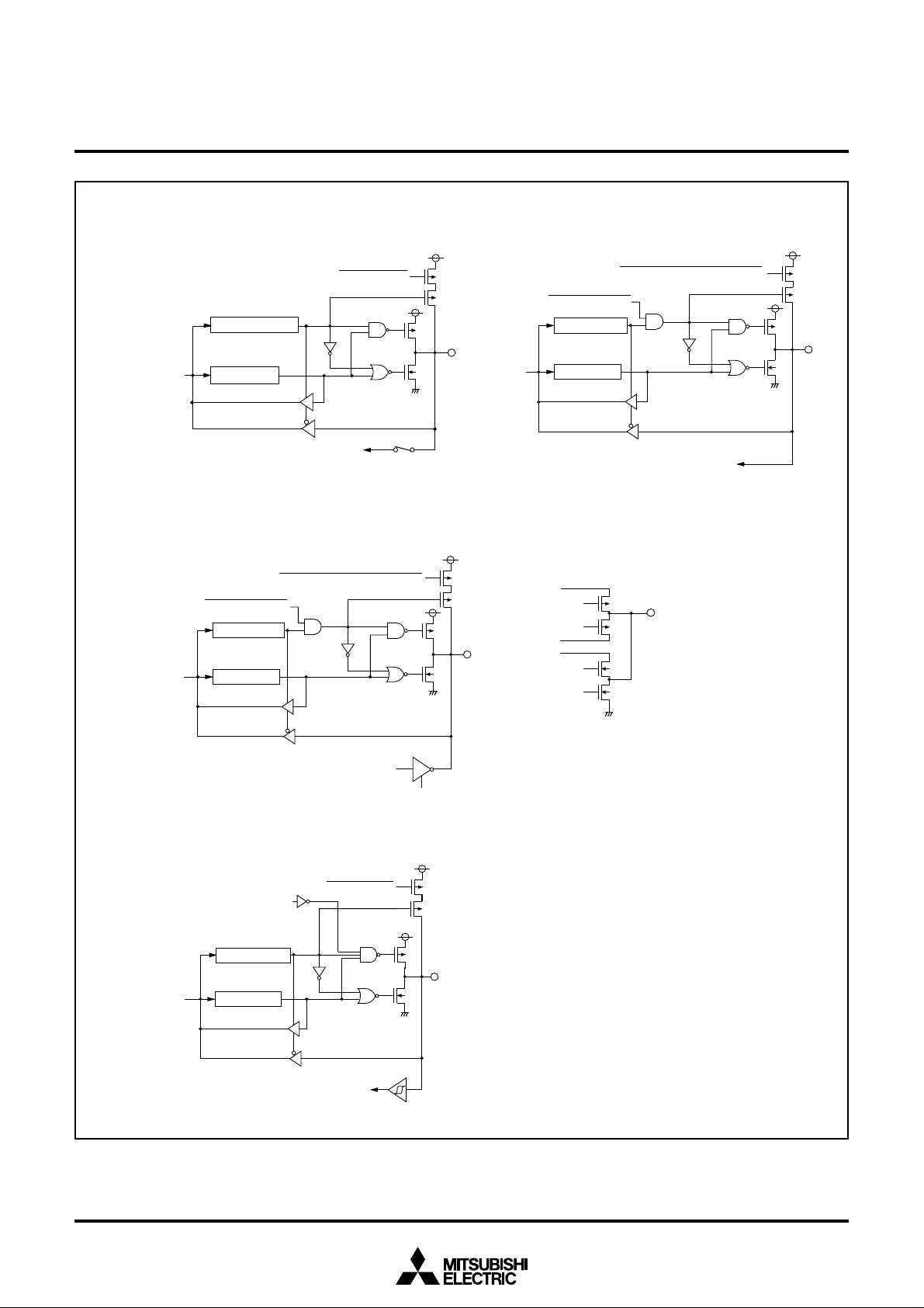
✽ ✽
✽ ✽
✽
✽
✽ ✽✽
✽ ✽✽
✽ ✽✽
✽ ✽✽
✽ ✽✽
✽ ✽
✽
Port P8
0
latch
Port P8
0
direction register = “0”
Port P8
1
latch
Port P8
1
direction register = “0”
Port P8
2
latch
Port P8
2
direction register = “0”
Port P8
3
latch
Port P8
3
direction register = “0”
Port P8
4
latch
Port P8
4
direction register = “1”
Port P8
5
latch
Port P8
5
direction register = “1”
Port P8
6
latch
Port P8
6
direction register = “1”
Port P8
7
latch
Port P8
7
direction register = “1”
P8
0
input
P8
1
input
P8
2
input
P8
3
input
P8
4
output
P8
5
output
P8
6
output
P8
7
output
PULL register A
Bit 5 = “1”
Port P8
Input reading circuit
Port PXx
“L” level output
✽ P-channel transistor for pull-up
✽ ✽ CMOS output buffer
Key input interrupt request
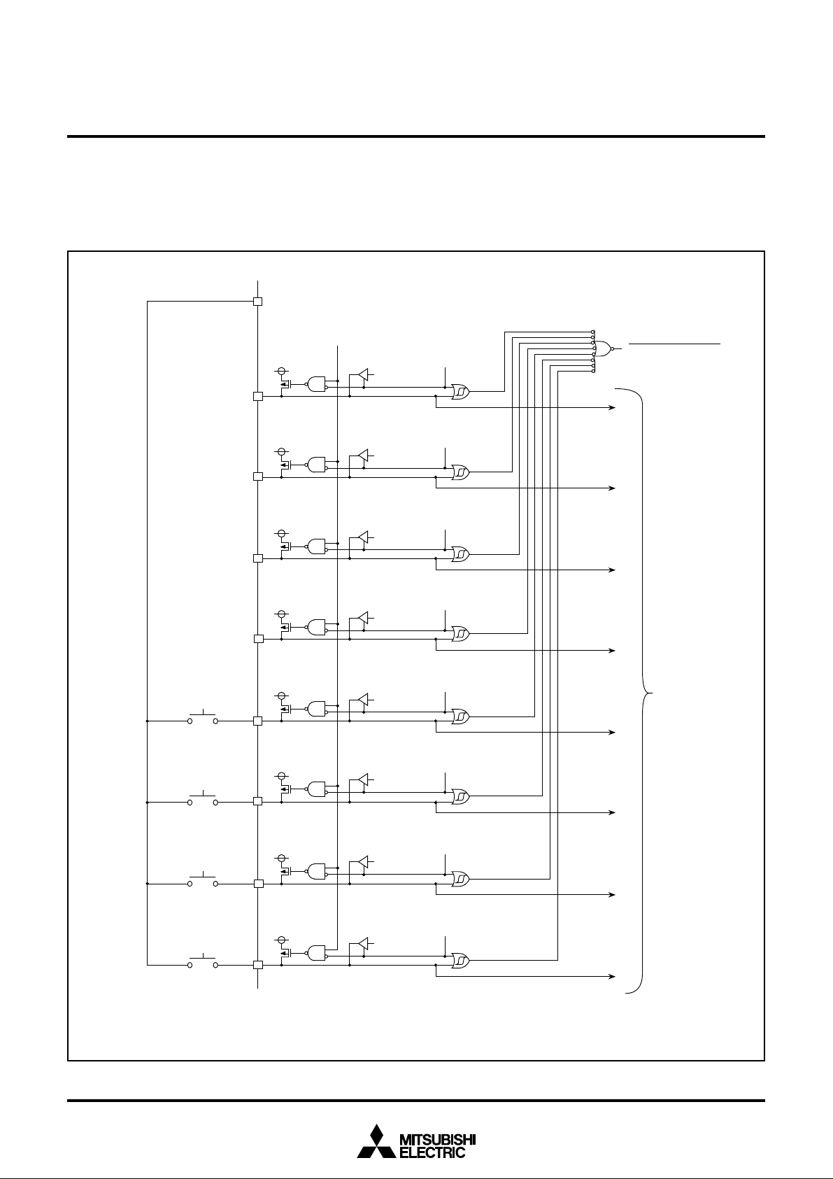
Key Input Interrupt (Key-on Wake-Up)
A key input interrupt request is generated by applying “L” level to any
pin of port P8 that have been set to input mode. In other words, it is
generated when AND of input level goes from “1” to “0”. An example
of using a key input interrupt is shown in Figure 15, where an inter-
rupt request is generated by pressing one of the keys consisted as
an active-low key matrix which inputs to ports P8
0–P83.
Fig. 15 Connection example when using key input interrupt and port P8 block diagram
19
SINGLE-CHIP 8-BIT CMOS MICROCOMPUTER
MITSUBISHI MICROCOMPUTERS
38C3 Group
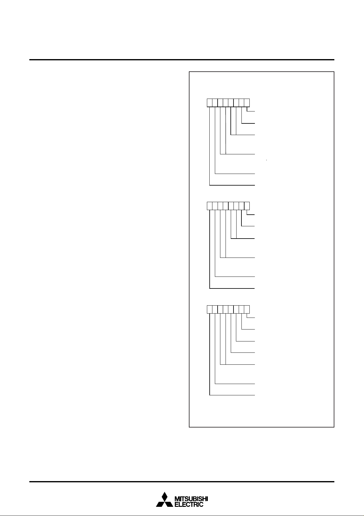
Timer 12 mode register
(T12M: address 0028
16
)
Timer 1 count stop bit
0 : Count operation
1 : Count stop
Timer 2 count stop bit
0 : Count operation
1 : Count stop
Timer 1 count source selection bits
00 : f(X
IN
)/16 or f(X
CIN
)/16
01 : f(X
CIN
)
10 : f(X
IN
)/32 or f(X
CIN
)/32
11 : f(X
IN
)/128 or f(X
CIN
)/128
Timer 2 count source selection bits
00 : Underflow of Timer 1
01 : f(X
CIN
)
10 : External count input CNTR
0
11 : Not available
Timer 1 output selection bit (P4
1
)
0 : I/O port
1 : Timer 1 output
Not used (returns “0” when read)
(Do not write “1” to this bit.)
Timer 34 mode register
(T34M: address 0029
16
)
Timer 3 count stop bit
0 : Count operation
1 : Count stop
Timer 4 count stop bit
0 : Count operation
1 : Count stop
Timer 3 count source selection bits
00 : f(X
IN
)/16 or f(X
CIN
)/16
01 : Underflow of Timer 2
10 : f(X
IN
)/32 or f(X
CIN
)/32
11 : f(X
IN
)/128 or f(X
CIN
)/128
Timer 4 count source selection bits
00 : f(X
IN
)/16 or f(X
CIN
)/16
01 : Underflow of Timer 3
10 : External count input CNTR
1
11 : Not available
Timer 3 output selection bit (P4
2
)
0 : I/O port
1 : Timer 3 output
Not used (returns “0” when read)
(Do not write “1” to this bit.)
Timer 56 mode register
(T56M: address 002A
16
)
Timer 5 count stop bit
0 : Count operation
1 : Count stop
Timer 6 count stop bit
0 : Count operation
1 : Count stop
Timer 5 count source selection bit
0 : f(X
IN
)/16 or f(X
CIN
)/16
1 : Underflow of Timer 4
Timer 6 operation mode selection bit
0 : Timer mode
1 : PWM mode
Timer 6 count source selection bits
00 : f(X
IN
)/16 or f(X
CIN
)/16
01 : Underflow of Timer 5
10 : Underflow of Timer 4
11 : Not available
Timer 6 (PWM) output selection bit (P5
2
)
0 : I/O port
1 : Timer 6 output
Not used (returns “0” when read)
(Do not write “1” to this bit.)
b7
b0
b7
b0
b7
b0
TIMERS
8-Bit Timer
The 38C3 group has six built-in timers : Timer 1, Timer 2, Timer 3,
Timer 4, Timer 5, and Timer 6.
Each timer has the 8-bit timer latch. All timers are down-counters.
When the timer reaches “00
16,” an underflow occurs with the next
count pulse. Then the contents of the timer latch is reloaded into the
timer and the timer continues down-counting. When a timer
underflows, the interrupt request bit corresponding to that timer is
set to “1.”
The count can be stopped by setting the stop bit of each timer to “1.”
The system clock φ can be set to either the high-speed mode or low-
speed mode with the CPU mode register. At the same time, timer
internal count source is switched to either f(X
IN) or f(XCIN).
●Timer 1, Timer 2
The count sources of timer 1 and timer 2 can be selected by setting
the timer 12 mode register. A rectangular waveform of timer 1 under-
flow signal divided by 2 is output from the P4
1/T1OUT pin. The wave-
form polarity changes each time timer 1 overflows. The active edge
of the external clock CNTR
0 can be switched with the bit 6 of the
interrupt edge selection register.
At reset or when executing the STP instruction, all bits of the timer 12
mode register are cleared to “0,” timer 1 is set to “FF
16,” and timer 2 is
set to “01
16.”
●Timer 3, Timer 4
The count sources of timer 3 and timer 4 can be selected by setting
the timer 34 mode register. A rectangular waveform of timer 3 under-
flow signal divided by 2 is output from the P4
2/T3OUT pin. The wave-
form polarity changes each time timer 3 overflows. The active edge
of the external clock CNTR
1 can be switched with the bit 7 of the
interrupt edge selection register.
●Timer 5, Timer 6
The count sources of timer 5 and timer 6 can be selected by setting
the timer 56 mode register. A rectangular waveform of timer 6 under-
flow signal divided by 2 can be output from the P5
2/PWM1 pin.
●Timer 6 PWM1 Mode
Timer 6 can output a rectangular waveform with “H” duty cycle n/
(n+m) from the P5
2/PWM1 pin by setting the timer 56 mode register
(refer to Figure 17). The n is the value set in timer 6 latch (address
0025
16) and m is the value in the timer 6 PWM register (address
0027
16). If n is “0,” the PWM output is “L,” if m is “0,” the PWM output
is “H” (n = 0 is prior than m = 0). In the PWM mode, interrupts occur
at the rising edge of the PWM output.
Fig. 16 Structure of Timer Related Register
Loading...