


APPLICATION NOTE |
Silicon RF Power Semiconductors |
|
|
|
|
|
Document NO. AN-VHF-051-B |
|
|
||
|
Date |
: 30th Sep. 2010 |
|
Rev. date |
: 7th Feb. 2011 |
|
Prepared |
: H.Sakairi |
|
|
K.Mori |
|
Confirmed |
: T.Okawa |
|
(Taking charge of Silicon RF by |
|
|
|
MIYOSHI Electronics) |
SUBJECT: RD04HMS2 single-stage amplifier with f=135-175MHz evaluation board
Features:
-The evaluation board for RD04HMS2
-Frequency: 135-175MHz
-Typical input power: 0.2W
-Typical output power: 5.5W
-Quiescent Current: 100mA
- Operating Current: 0.65A
-Surface-mounted RF power amplifier structure
Gate Bias |
|
Drain Bias |
RF IN |
|
RFOUT |
PCB L=80mm W=55mm
Application Note for Silicon RF Power Semiconductors
1/23
RD04HMS2 single-stage amplifier with f=135-175MHz evaluation board
- AN-VHF-051-B-
Contents
|
|
|
|
|
|
Page |
1. |
Equivalent Circuitry |
------------------------------------------------------------ |
|
|
3 |
|
2. |
PCB Layout ----------------------------------------------------------------------- |
|
|
|
4 |
|
3. |
Component List and -----------------------------------------Standard Deliverable |
5 |
||||
4. |
Thermal Design of Heat ------------------------------------------------Sink |
|
|
6 |
||
5. |
Typical RF Characteristics ---------------------------------------------------- |
|
|
7 |
||
|
5-1. |
Frequency vs. --------------------------------------------- |
(Vds=12.5V) |
|
7 |
|
|
5-2. |
RF Power vs. ------------------------------------------- |
(Vds=12.5V) |
|
8 |
|
|
5-3. |
Drain Quiescent ------------------------Current vs. |
(Vds=12.5V) |
12 |
||
|
5-4. |
DC Power Supply ----------------------------------vs. |
(Idq=0.1A) |
14 |
||
|
5-5. |
Frequency vs. --------------------------------------- |
(Vds=9.1V) |
|
17 |
|
|
5-6. |
RF Power vs. --------------------------------------- |
(Vds=9.1V) |
|
18 |
|
|
5-7. |
Drain Quiescent -------------------Current vs. |
(Vds=9.1V) |
22 |
||
Application Note for Silicon RF Power Semiconductors
2/23
RD04HMS2 single-stage amplifier with f=135-175MHz evaluation board
- AN-VHF-051-B-
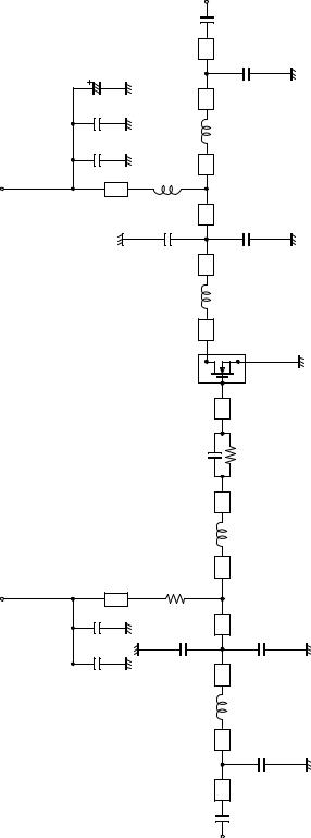
1.Equivalent Circuitry
RF-out
|
|
|
C9 |
|
|
|
|
C14 |
|
|
|
7.5mm |
C8 |
|
C13 |
|
|
|
2mm |
|
|
C12 |
L5 |
L4 |
|
5.5mm |
|
Vdd |
W |
|
|
|
|
|
|
21mm |
C7 |
|
|
3mm |
C6 |
|
|
|
|
|
4.5mm |
|
|
|
|
L3 |
|
|
|
|
|
|
|
|
3mm |
|
|
|
RD04HMS2 |
f=135MHz |
|
|
|
|
|
|
|
5.5mm |
|
|
|
|
|
C5 |
|
R2 |
|
|
|
|
|
4mm |
|
|
|
|
|
|
L2 |
|
|
|
21mm |
R1 |
1.5mm |
|
|
|
Vgg |
W |
|
|
|
|
|
|
|
|
|
4mm |
|
|
|
C11 |
|
|
|
|
|
|
C10 |
|
C4 |
0.5mm |
|
C3 |
|
|
|
|
L1 |
|
|
|
|
|
|
0.5mm |
|
|
|
|
|
|
8mm |
|
C2 |
|
|
|
|
C1 |
|
|
|
|
|
|
|
RF-in |
|
W:Line width=1.0mm
Micro strip line width=1.3mm/50OHM,er:4.8,t=0.8mm
Note:Board material- Glass-Epoxy Substrate
Application Note for Silicon RF Power Semiconductors
3/23

RD04HMS2 single-stage amplifier with f=135-175MHz evaluation board
- AN-VHF-051-B-
2.PCB Layout
BOARD OUTLINE: 80.0*55.0(mm)
MATERIAL : FR-4<R1705>
THICKNESS : 0.8(mm)
TOP VIEW
TOP VIEW ( Parts mounting )
|
|
|
|
|
|
|
|
22u |
|
|
|
|
1000p |
|
|
1000p |
|
|
|
|
|
|
|
|
|
|
|
|
|
|
|
|
1000p |
|
|
1000p |
|
|
|
|
4007C |
30p |
4.7Kohm |
2312A |
47ohm |
4005C |
39p |
4007C 4006C |
|
|
|
||||||||
100p |
CUT |
|
CUT |
36p |
CUT |
|
CUT |
100p |
|
27p |
30p |
CUT |
39p |
24p |
|||||
Application Note for Silicon RF Power Semiconductors
4/23

RD04HMS2 single-stage amplifier with f=135-175MHz evaluation board
- AN-VHF-051-B-
3.Component List and Standard Deliverable
-Component List
No. |
|
Description |
|
|
P/N |
Qty |
Manufacturer |
Tr |
|
MOSFET |
|
|
RD04HMS2 |
1 |
Mitsubishi Electric Corporation |
C |
1 |
100 pF |
2012 |
50V |
GRM2162C1H101JA01D |
1 |
MURATA MANUFACTURING CO. |
C |
2 |
27 pF |
2012 |
50V |
GRM2162C1H270JZ01D |
1 |
MURATA MANUFACTURING CO. |
C |
3 |
30 pF |
2012 |
50V |
GRM2162C1H300JZ01D |
1 |
MURATA MANUFACTURING CO. |
C |
4 |
30 pF |
2012 |
50V |
GRM2162C1H300JZ01D |
1 |
MURATA MANUFACTURING CO. |
C |
5 |
36 pF |
2012 |
50V |
GRM2162C1H360JZ01D |
1 |
MURATA MANUFACTURING CO. |
C |
6 |
39 pF |
2012 |
50V |
GRM2162C1H390JZ01D |
1 |
MURATA MANUFACTURING CO. |
C |
7 |
39 pF |
2012 |
50V |
GRM2162C1H390JZ01D |
1 |
MURATA MANUFACTURING CO. |
C |
8 |
24 pF |
2012 |
50V |
GRM2162C1H240JZ01D |
1 |
MURATA MANUFACTURING CO. |
C |
9 |
100 pF |
2012 |
50V |
GRM2162C1H101JA01D |
1 |
MURATA MANUFACTURING CO. |
C |
10 |
1000 pF |
1608 |
50V |
GRM188R11H102KA01E |
1 |
MURATA MANUFACTURING CO. |
C |
11 |
1000 pF |
1608 |
50V |
GRM188R11H102KA01E |
1 |
MURATA MANUFACTURING CO. |
C |
12 |
1000 pF |
1608 |
50V |
GRM188R11H102KA01E |
1 |
MURATA MANUFACTURING CO. |
C |
13 |
1000 pF |
1608 |
50V |
GRM188R11H102KA01E |
1 |
MURATA MANUFACTURING CO. |
C |
14 |
22 uF |
|
50V |
H1002 |
1 |
NICHICON CORPORATION |
L |
1 |
37 nH * |
Diameter: Wire=0.4mm Inside=1.6mm T/N of coils=7 |
1 |
YC CORPORATION Co.,Ltd. |
||
L |
2 |
56 nH * |
Diameter: Wire=0.23mm Inside=1.1mm T/N of coils=12 |
1 |
YC CORPORATION Co.,Ltd. |
||
L |
3 |
22 nH * |
Diameter: Wire=0.4mm Inside=1.6mm T/N of coils=5 |
1 |
YC CORPORATION Co.,Ltd. |
||
L |
4 |
29 nH * |
Diameter: Wire=0.4mm Inside=1.6mm T/N of coils=6 |
1 |
YC CORPORATION Co.,Ltd. |
||
L |
5 |
37 nH * |
Diameter: Wire=0.4mm Inside=1.6mm T/N of coils=7 |
1 |
YC CORPORATION Co.,Ltd. |
||
R |
1 |
4.7k ohm |
2012 |
|
RPC10T472J |
1 |
TAIYOSHA ELECTRIC CO. |
R |
2 |
47 ohm |
1608 |
|
RPC05N470J |
1 |
TAIYOSHA ELECTRIC CO. |
Pb |
|
PCB |
|
|
MS3A0166 |
1 |
Homebuilt |
Rc |
|
SMA |
female connector |
HRM-300-118S |
2 |
HIROSE ELECTRIC CO.,LTD |
|
Bc |
1 |
Bias connector |
red color |
TM-605R |
2 |
MSK Corporation |
|
Bc |
2 |
Bias connector |
black color |
TM-605B |
2 |
MSK Corporation |
|
Pe |
|
Aluminum pedestal |
|
|
1 |
Homebuilt |
|
|
|
Conducting wire |
|
|
4 |
Homebuilt |
|
|
|
Screw |
M2 |
|
|
16 |
- |
*Inductor of Rolling Coil measurement condition : f=100MHz
-Standard Deliverable
TYPE1 |
Evaluation Board assembled with all the component |
TYPE2 |
PCB (raw board) |
Application Note for Silicon RF Power Semiconductors
5/23

RD04HMS2 single-stage amplifier with f=135-175MHz evaluation board
- AN-VHF-051-B-
4.Thermal Design of Heat Sink
Tr |
|
|
|
Junction point of MOSFET chip |
|||
|
|||||||
Pb |
|
|
|
|
|
|
(in this package) |
|
|
|
|
|
|
||
|
|
|
|
||||
|
|
|
|
|
|
Rth(ch-Pb bottom)=Rth(ch-case)+Rth(case-Pb bottom) |
|
|
|
|
|
|
|
|
=5.0 (deg. C./W) |
|
|
|
|
|
|
||
Pe |
|
|
|
|
|
|
|
|
|
|
|
|
|
|
|
Tch(delta)=(Pout/Efficiency-Pout+Pin) x Rth(ch-Pb bottom)=(4W/50%-4W+0.2) x 5.0 = 21 (deg. C.) Also, operating Tj (“Tj(op)”)=120 (deg. C.), in case of RD series that Tch(max) = 150 (deg. C.) Therefore TPb bottom-air as delta temperature between Pb bottom and the ambient 60 deg. C. TPb bottom-air=“Tj(op)”- Tch(delta) - Ta(60deg.C.)=120-21-60=39 (deg. C.)
In terms of long-term reliability, “Tj(op)” has to be kept less than 120 deg. C. i.e. TPb bottom-air has to be less than 39 deg. C..
The thermal resistance of the heat sink to border it:
Rth(Pb bottom-air)=TPb bottom-air/(Pout/Efficiency-Pout+Pin)=39/(4W/50%-4W+0.2)= 9.3 (deg. C./W) Therefore
it is preferable that the thermal resistance of the heat sink is much smaller than 9.3 deg. C./W.
Application Note for Silicon RF Power Semiconductors
6/23

RD04HMS2 single-stage amplifier with f=135-175MHz evaluation board
- AN-VHF-051-B-
5. Typical Performance
5-1. Frequency vs.
OUTPUT POWER, POWER GAIN, DRAIN EFFICIENCY, DRAIN CURRENT and INPUT RETURN LOSS
(Vds=12.5V) |
|
|
|||
|
|
Ta=+25deg.C |
|
|
|
|
18 |
Vds=12.5V, Idq=0.1A, Pin=0.2W |
90 |
|
|
|
|
|
|||
|
16 |
ηD |
80 |
|
|
|
14 |
Gp |
70 |
|
|
Pout(W) , Gp(dB) |
12 |
|
60 |
Drain Effi(%) |
|
10 |
|
50 |
|||
8 |
Pout |
40 |
|||
6 |
30 |
||||
|
|||||
|
4 |
|
20 |
|
|
|
2 |
|
10 |
|
|
|
0 |
|
0 |
|
|
|
130 135 140 145 150 155 160 165 170 175 180 |
|
|||
|
|
f (MHz) |
|
|
|
Ta=+25deg.C |
|
|
|
Vds=12.5V, Idq=0.1A, Pin=0.2W |
5 |
|
|
40 |
|
|
|
|
Pout |
|
|
|
Idd |
0 |
R. L. (dB) , Idd(A) |
|
|
||
30 |
|
|
|
Pout(dBm) |
|
-5 |
|
|
-10 |
||
20 |
|
|
Input |
|
I.R.L. |
-15 |
|
|
|
|
|
10 |
|
-20 |
|
130 135 140 145 150 |
155 160 165 170 175 180 |
|
|
f (MHz) |
|
|
|
Ta=+25deg. C., Vds=12.5V, Idq=0.1A, Pin=0.2W
Freq. |
Vgg |
Pin |
|
Pout |
Gp |
ID(RF) |
ηadd |
ηD |
I.R.L. |
||
(MHz) |
(V) |
(dBm) |
|
(W) |
(dBm) |
(W) |
(dB) |
(A) |
(%) |
(%) |
(dB) |
|
|
|
|
|
|
|
|
|
|
|
|
130 |
2.66 |
23.0 |
|
0.2 |
37.4 |
5.4 |
14.3 |
0.64 |
65.6 |
68.1 |
-6.8 |
135 |
2.66 |
23.1 |
|
0.2 |
37.6 |
5.8 |
14.6 |
0.64 |
70.1 |
72.7 |
-8.2 |
140 |
2.66 |
23.0 |
|
0.2 |
37.8 |
6.0 |
14.8 |
0.63 |
74.2 |
76.8 |
-9.7 |
145 |
2.66 |
23.0 |
|
0.2 |
37.8 |
6.1 |
14.8 |
0.61 |
76.7 |
79.4 |
-10.9 |
150 |
2.66 |
23.1 |
|
0.2 |
37.8 |
6.1 |
14.7 |
0.60 |
78.0 |
80.7 |
-11.6 |
155 |
2.66 |
23.0 |
|
0.2 |
37.8 |
6.0 |
14.7 |
0.58 |
80.6 |
83.4 |
-11.8 |
160 |
2.66 |
23.0 |
|
0.2 |
37.8 |
6.0 |
14.7 |
0.58 |
80.1 |
82.9 |
-11.9 |
165 |
2.66 |
23.1 |
|
0.2 |
37.8 |
6.0 |
14.7 |
0.58 |
80.1 |
82.9 |
-12.5 |
170 |
2.66 |
23.0 |
|
0.2 |
37.8 |
6.0 |
14.8 |
0.58 |
80.5 |
83.3 |
-13.8 |
175 |
2.66 |
23.1 |
|
0.2 |
37.8 |
6.1 |
14.8 |
0.59 |
80.0 |
82.7 |
-16.3 |
180 |
2.66 |
23.0 |
|
0.2 |
37.9 |
6.1 |
14.9 |
0.59 |
80.4 |
83.1 |
-17.7 |
Application Note for Silicon RF Power Semiconductors
7/23
 Loading...