


DVR-6300
In compliance with Federal Regulations, following are repro-
duction of labels on, or inside the product relating to laser
product safety.
KENWOOD Corp. certifies this equipment conforms to DHHS
Regulations No.21 CFR 1040. 10, Chapter 1, subchapter J.
DANGER : Laser radiation when open and interlock defeated.
AVOID DIRECT EXPOSURE TO BEAM.
Caution : No connection of ground line if disassemble
the unit. Please connect the ground line on
rear panel, PCBs, Chassis and some others.
DVD AV CONTROL CENTER
DVR-6300
SERVICE MANUAL
(DVT-6300/7300/8300)
© 2004-8 PRINTED IN KOREA
B51-5922-00 (K/K) 746
70%
POWER
Panel ass’y *
(A60-)
Door
(A29-1243-08)
Knob
(K29-8412-08)
Fiber opt jack
(W02-4590-08)
Jack RCA
(E59-0001-08)
Cabinet
(A01-3942-08)
Tuner *
(W02-)
Phone jack
(E11-0989-08)
Jack RCA *
(E63-)
Terminal block
(E70-1003-08)
* Refer to parts list on page 27.
CAUTION:
Use of controls or adjustments or performance of procedures
other than those specified herein may result in hazardous radia-
tion exposure.
In compliance with Federal Regulations, the following are repro-
ductions of labels on, or inside the product relating to laser prod-
uct safety.
KENWOOD CORPORATION
2967-3, ISHIKAWA-CHO,
HACHIOJI-SHI,
TOKYO, JAPAN
KENWOOD CORP. CERTIFIES THIS EQUIPMENT
CONFORMS TO DHHS REGULATIONS NO. 21 CFR
1040.10, CHAPTER 1, SUBCHAPTER J.
Location: Back Panel
For the U.S.A.
For Canada
NOTICE: This Class B digital apparatus complies with
Canadian ICES-003.
Note to CATV system installer
This reminder is provided to call the CATV system installer’s at-
tention to Article 820-40 of the NEC that provides guidelines for
proper grounding and, in particular, specifies that the cable
ground shall be connected to the grounding system of the build-
ing, as close to the point of cable entry as practical.
For the U.S.A.
Caution on condensation
Before transporting or moving this unit, carry out the
following operations.
1. Set the POWER ON/OFF switch to the ON
without loading a disc.
2. Wait a few seconds and verify that the display
shown appears.
"NO DISC"
3. Set the POWER ON/OFF switch to OFF.
Note related to transportation and movement
Condensation (of dew) may occur inside the unit when there is a great
difference in temperature between this unit and the outside. This unit
may not function properly if condensation occurs. In this case, leave
the unit for a few hours and restart the operation after the condensa-
tion has dried up.
Be specially cautious against condensation in the following circum-
stances:
When this unit is carried from one place to another across a large
difference in temperature, when the humidity in the room where
this unit is installed increases, etc.
Operation to reset
The microprocessor may fall into malfunction
(impossibility to operate erroneous display, etc.)
when the power cord is unplugged while power is
ON or due to an external factor.
In this case, switch off the power, wait for several
seconds, and then switch the power on again.
The marking of products using lasers
(For countries other than U.S.A. and Canada)
The marking this product has been classified as Class 1. It
means that there is no danger of hazardous radiation outside
the product.
Location: Back panel
CLASS 1
LASER PRODUCT
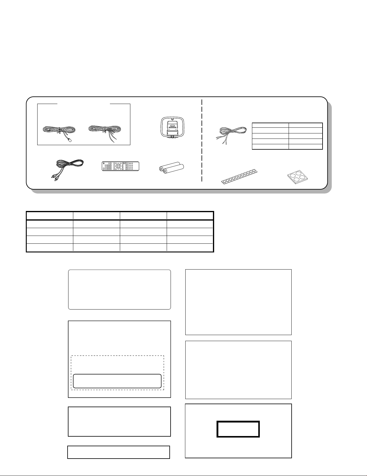
Video cord (Yellow)(1)
(E30-7341-08)
Loop antenna (1)
(T90-0917-08)
FM indoor antenna (1)
Remote control unit (1)
(A70-1685-08)
Batteries
(R03/AAA) (2)
Speaker cords (6) *
(For Europe)
(T90-0916-08)
(For U.S.A., Canada
and Australia)
(T90-0915-08)
Accessories for speaker part
(For DVT-6300 and DVT-7300)
Length
For Front (2) 4.5 m (177-3/16")
For Center (1) 3 m (118-1/8")
For Rear (2) 8 m (314-15/16")
For Subwoofer (1) 4.5 m (177-3/16")
Cushion (15) *
(Small : 11 pcs 1 sheet) (Big : 4 pcs 1 sheet)
* See speaker’s manual.
DVR-6300
2
CONTENTS / ACCESSORIES / CAUTIONS
CONTENTS / ACCESSORIES / CAUTIONS...............2
PARTS DESCRIPTIONS .............................................3
PC BOARD ..................................................................4
SCHEMATIC DIAGRAM ............................................15
EXPLODED VIEW .....................................................25
PARTS LIST...............................................................27
SPECIFICATIONS .....................................................34
CONTENTS
ACCESSORIES
CAUTIONS
SYSTEM CONFIGURATIONS
SYSTEM RECEIVER SPEAKER SPEAKER
DVT-6300-H DVR-6300 KSW-6300-H -
DVT-6300-S DVR-6300 KSW-6300-S -
DVT-7300 DVR-6300 KSW-7300 -
DVT-8300 DVR-6300 KS-908HT SW-18HT
DVR-6300
3
PARTS DESCRIPTIONS
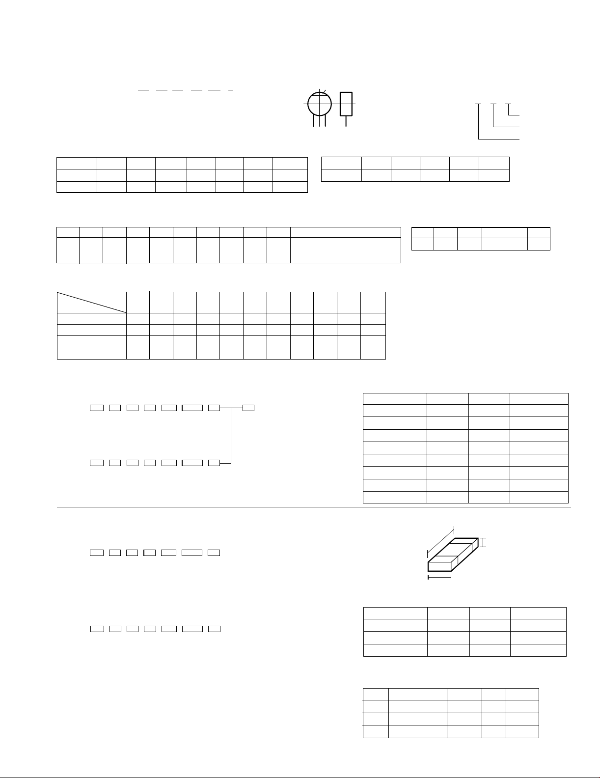
CAPACITORS CC 45 TH 1H 220 J
123 4 5 6
1 = Type ... ceramic, electrolytic, etc. 4 = Voltage rating
2 = Shape ... round, square, ect. 5 = Value
3 = Temp. coefficient 6 = Tolerance
• Temperature coefficient
1st Word C L P R S T U
Color* Black Red Orange Yellow Green Blue Violet
ppm/°C 0 -80 -150 -220 -330 -470 -750
2nd Word G H J K L
ppm/°C ±30 ±60 ±120 ±250 ±500
Example : CC45TH = -470 ± 60ppm/°C
• Tolerance (More than 10pF)
Code C D G J K M X Z P No code
(%) ±0.25 ±0.5 ±2 ±5 ±10 ±20 +40 +80 +100 More than 10µF - 10 ~ +50
-20 -20 -0 Less than 4.7µF -10 ~ +75
(Less than 10pF)
Code B C D F G
(pF) ±0.1 ±0.25 ±0.5 ±1 ±2
2nd word
ABCDEFGHJKV
1st word
0 1.0 1.25 1.6 2.0 2.5 3.15 4.0 5.0 6.3 8.0 -
1 10 12.5 16 20 25 31.5 40 50 63 80 35
2 100 125 160 200 250 315 400 500 630 800 -
3 1000 1250 1600 2000 2500 3150 4000 5000 6300 8000 -
• Voltage rating
• Chip capacitors
Refer to the table above.
1 = Type
2 = Shape
3 = Dimension
4 = Temp. coefficient
5 = Voltage rating
6 = Value
7 = Tolerance
Dimension (Chip capacitors)
Dimension code L W T
Empty 5.6 ± 0.5 5.0 ± 0.5 Less than 2.0
A 4.5 ± 0.5 3.2 ± 0.4 Less than 2.0
B 4.5 ± 0.5 2.0 ± 0.3 Less than 2.0
C 4.5 ± 0.5 1.25 ± 0.2 Less than 1.25
D 3.2 ± 0.4 2.5 ± 0.3 Less than 1.5
E 3.2 ± 0.2 1.6 ± 0.2 Less than 1.25
F 2.0 ± 0.3 1.25 ± 0.2 Less than 1.25
G 1.6 ± 0.2 0.8 ± 0.2 Less than 1.0
RESISTORS
• Chip resistor (Carbon)
Dimension
• Carbon resistor (Normal type)
1 = Type 5 = Rating wattage
2 = Shape 6 = Value
3 = Dimension 7 = Tolerance
4 = Temp. coefficient
Dimension (Chip resistor)
Dimension code L W T
E 3.2 ± 0.2 1.6 ± 0.2 1.0
F 2.0 ± 0.3 1.25 ± 0.2 1.0
G 1.6±0.2 0.8±0.2 0.5±0.1
Rating wattage
Code Wattage Code Wattage Code Wattage
1J 1/16W 2C 1/6W 3A 1W
2A 1/10W 2E 1/4W 3D 2W
2B 1/8W 2H 1/2W
CC45
Color*
• Capacitor value
010 = 1pF
100 = 10pF
101 = 100pF
102 = 1000pF = 0.001µF
103 = 0.01µF
2 2 0 = 22pF
Multiplier
2nd number
1st number
C C 7 3 0 0 01 HS LFJ
1
(Chip)
234 5 6 7
(CH, RH, UJ, SL)
(Chip)
(B, F)
(EX)
C K 7 3 0 0 01 HFFZ
12345 6 7
(EX)
R K 7 3 0 0 02 BBEJ
1
(Chip)
234 5 6 7
(B,F)
(EX)
R D 1 4 0 0 02 CBBJ
12345 6 7
(EX)
L
T
W
4
A BDCE
2
1
3
5
7
4
6
Refer to the schematic diagram for the value of resistors and capacitors.
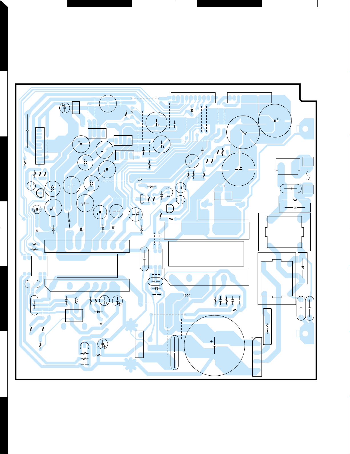
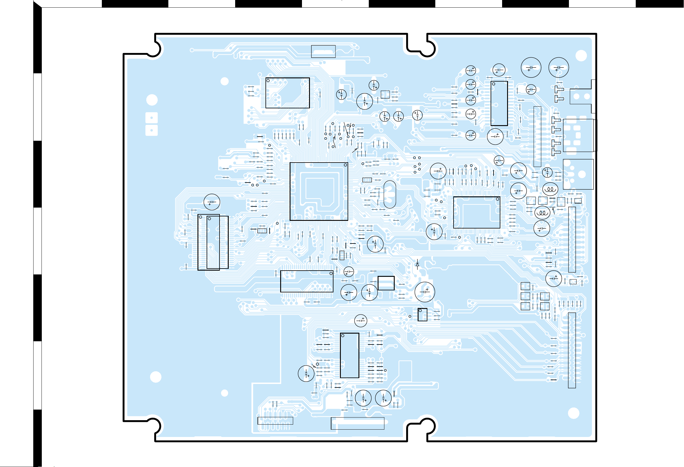
PC BOARD
(
Component side view
)
CN902
CN901
IC921
IC922
IC923
D942
IC924
D929
D928
CN903
D951
PN901
Q921
D933
Q922
IC941
D922
D921
PC911
PC910
D924
D923
D926
D927
ZD911
Q910
IC901
D902
PC921
IC902
D901
D911
BD901
D912
D903
D932
ZD921
IC942
D941
W930
C935
W929
C953
C952
FH900B
FH900A
F901
C943
R949
W932
C914
C915
W905
R913
C904
W902
R904
R905
R906
EB
1
4
C909
FB902
C944
W910
W909
R941
R942
W906
C910
L923
C924
C925
C926
C927
C930
C942
W907
C922
C923
C929
C941
VR901
R900
CM901
C951
C954
C940
R946
R947
R948
R950
R921
EB
EB
R922
W921
C900
T901
W922
T902
LF902
CM902
C902
C901
LF901
TH901
C921
R912
R911
W901
C913
C911
15
W904
R903
R902
C907
C908
FB901
W916
W913
C905
R901
R909
R910
W903
R952
R954
R953
R951
W920
C938
W928
W927
10
1
14
14
14
10
OGI
1
31
31
10 1
W926
W925
W924
W923
C936
W914
W915
C932
R934
C937
W918
W911
C933
W912
W917
W931
W919
L922
L921
R933
R943
R944
R945
C939
C934
R932
C928
W908
SMPS
2
FHJ LNGIKMO
1
3
5
7
4
6
PDA03
PDM01
Q203
Q201
Q205
Q204
Q6C3Q6C2Q6C5
Q6C1
Q202
Q6C4
PDA02
J6
PDM02
PDA01
JK6A3
JK6A2
JK6A1
ZD6A4
ZD6A3
ZD6A2
ZD6A1
ZD6A5ZD6A6
IC506
IC502
IC503
IC501
IC5A1
IC202
IC570
D501
IC505
IC201
IC5C1
Q501
R211
C211
C241
C639
C641
TP223
C528
C5C6
C545
C543
C541
C511
C5A1
C293
TP224
TP206
C6A4
C6A1
C208
L201
L203
C292
C564
C598
C291
C5C7
C5C5
C5C4
C5C3
C5C2
C5C9
C6A5
C6A6
C295
C207
C206
C5C1
C583
C242
C563
C559
C558
C557
C561
R726
R725
R724
R723
R722
R721
C515
R720
R719
R567
C5A2
L504
C505
C504
C538
C537
C507
C508
C509
C510
TP219
TP220
TP207
TP209
C540
C539
R503
C531
TP–RERPC
R529
L501
C281
C279
R255
R254
C274
R252
C271
C252
R259
R253
C278
C277
C267
C273
C272
R258
R5C7
R5C8
C270
C268
C269
C251
C266
C283
L5C1
R620
L204
EB
S
D
G
EB
BE
C203
L205
R202
R6C4
BEBEBE
BE
GS
D
BE
R6C2
R6C6
R6C3
R6C7
R6C8
R6C5
R6C1
C567
R525
R524
C566
R528
C568
R523
C565
C202
R203
R204
R619
R617
R618
TP212
TP213
TP214
C253
C254
C255
R577
R575
R574
C526
C525
C577
C578
C579
C576
C239
L604
C640
C642
L231
C214
R218
C644
L603
C524
C523
R520
C522
C521
R506
C597
R573
R572
F501
C555
R582
R508
27MHz
X501
C534
R527
BE
R566
C512
R565
R564
C506
R502
TP222
TP546
TP544
TP545
R504
C513
TP552
TP551
TP550
TP549
TP548
TP547
TP221
C514
R522
TP MA11
F500
C589
C556
R579
R569
C560
R583
R519
R517
R515
TP URD#
TP UWR#
TP ALE
R581
R521
C520
R518
R516
C519
TP553
C518
R735
R734
C517
R732
R730
R729
R728
R727
R501
C502
C503
C592
R514
C536
R513
C542
R511
C535
F502
R584
C533
R510
R509
C532
C530
R552
R553
R551
R550
C280
R256
L262
L263
L264
L265
C267
C282
R621
R616
R6A3
R6A4
C6A2
R222
R221
R206
R201
R207
R220
R210
C265
C264
C263
C262
R251
C259
C258
L202
R209
R6E1
R6E2
R6E3
R6E4
R6E5
R6E6
R6E7
C201
R257
R219
R205
R208
C6A3
R6A2
L261
R6A1
R6A5
R5C6
R5C5
R5E0
R5C4
R5C9
R5E2
R5C3
R5C2
R5C1
C5C8
C5E0
R5E1
C256
C257
C260
C261
C574R543
R571
R576
R539
C554
L502
C582
R570
R555
R556
R557
R534
R535
C575
TP521
L251
R216 R213
R245 R212
R244 R246
R243 C240
R242 R241
R240 C243
C643
C637
C638
C645
R237
R239
R238
C244
C581 C580
R231
R232
C231
R233
R234
C233
C234
R215
C296
R217
C213
R214
TP558
C232
C212
R236R235
C245
R578
C529
C527
R507
C544
TP218
TP217
TP215
TP216
R512
R526
C569
R505
C516
R5A9
R5A8
R5A7
R736
R737
R733
R731
R580
R568
127
54
125
5026
28
125
5026
154
162
163
216
108
55
109
1
14
24
48
25
1
1
2
10
11
110
18
36
19
1
4
8
1
123
119
2
20
222
25
2
26
5
138
102
65
39
64
128
103
1
14
28
15
DVD
Refer to the schematic diagram for the value of resistors and capacitors.
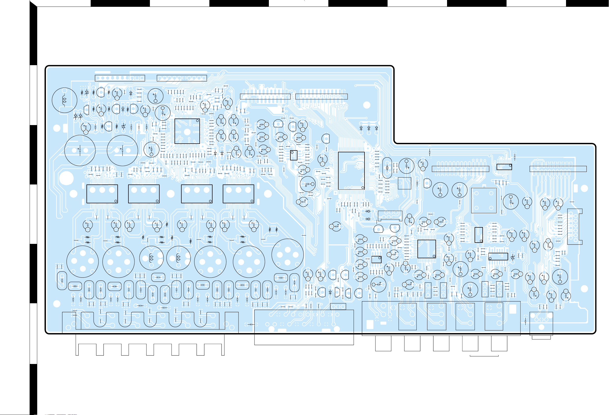
PC BOARD
(
Component side view
)
5 6
P QSUWYRTVX
2
1
3
5
7
4
6
TP522
TP523
TP540
TP542
TP541
TP520
TP524
TP526
TP530
TP535
TP512
TP511
TP509
TP532
TP531
TP202
TP203
TP201
TP225
TP205
TP204
TP226
TP559
TP513
TP508
TP507
TP506
TP505
TP504
TP503
TP502
TP501
TP528
TP518
TP514
TP533
TP515
TP510
TP537
TP519
TP516
TP517
TP539
DVD
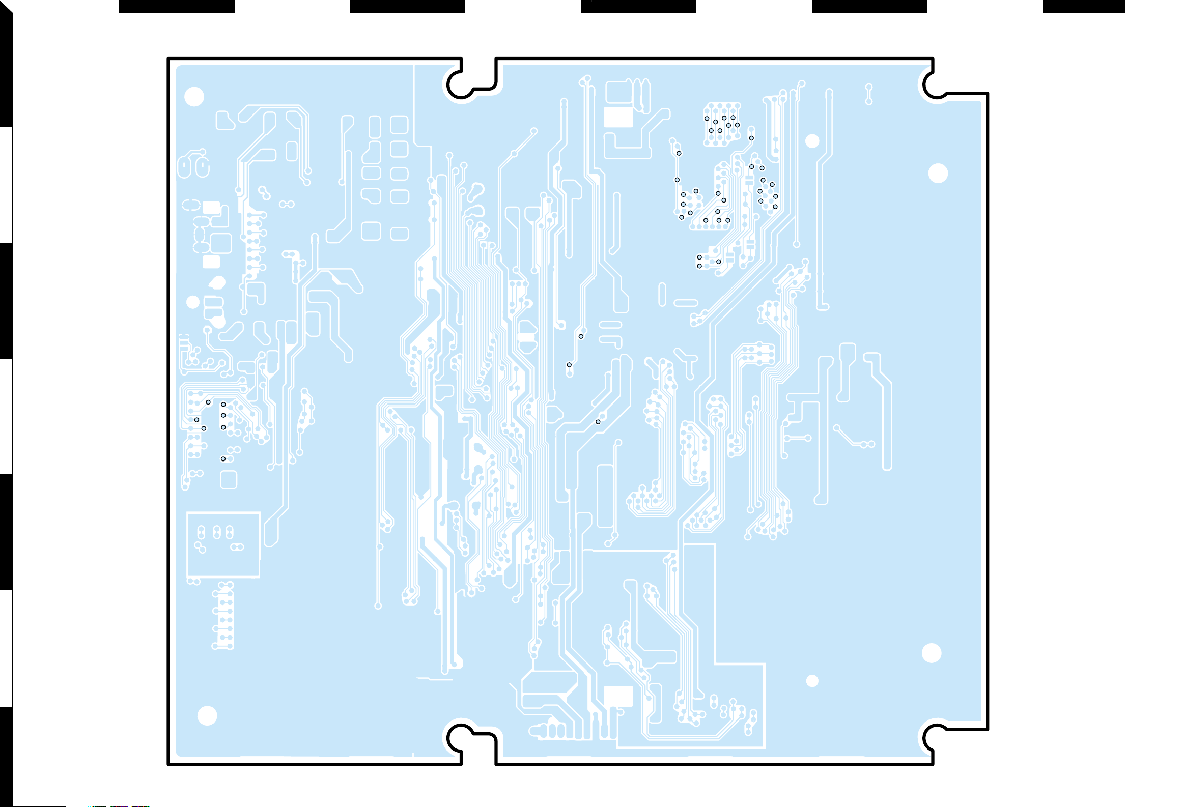
Refer to the schematic diagram for the value of resistors and capacitors.
PC BOARD
(
Foil side view
)
7 8
2
ZABADAFAHAA AC AE AG AI
1
3
5
7
4
6
IC301
IC730
IC770 IC750
IC710
IC101
IC201
IC601
IC202
IC203
IC501
IC503
ZD981
MAIN
D300
D103
Q506
D102
D104
D600
Q601
JK700
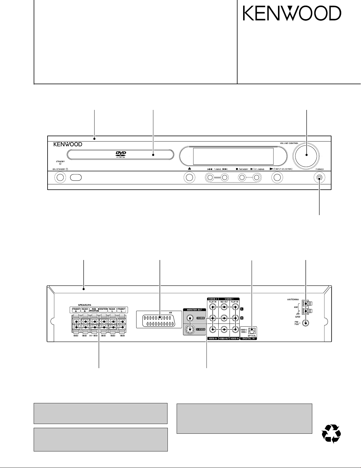
FRONT
R
REAR
R
SUB
WOOFER
CENTER REAR
L
FRONT
L
S VIDEO COMPONENT
VIDEO OUT
MONITOR
OUT
VIDEO2 OUT
VIDEO IN
IN
IN
OPTICAL
IN
JK602
JK601
Q605
Q606
Q604
Q603
Q602
Q101
PN103
ZD601
JK200
Q504
Q505
Q502
Q501
SW101
PN105
PN200
PN201
D105
D101
Q973
D981
D302
D301
ZD973
PN901
PN902
PN101
PN102
Q971
Q975
ZD971
Q972
Q982
ZD972
L700
C973
C338
C326
C981
C975
C701
C700
C736
L741
C843
C833
C863
C823
C699
C813
C617
FB617
R536
C618
C558
C610
C112
C508
FB502
FB501
C509
C603
C511
X201
FB503
C601
C214
C216
C207
C537
C690
C536
C522
C535
C546
C547
C548
C549
C561
C564
C563
C562
L721
L711
C871
L761
C798
C799
L731
L771
L781
R765
C775
C785
R984
R983
R979
R976
C989
C991
C990
R980
R973
R972
R978
C974
C333
C330
C335
C332
X101
C101
C107
C102
C524
C523
C525
C111
C622
C623
C205
C203
C619
C605
C201
C218
C620
C621
122
111
C108
C602
C609
FB504
C608
C298
VIDEO1 IN
VIDEO1 OUT
VIDEO2 IN
COMPONENT
C209
C213
C297
C106
C105
C334
C324
C340
C331
C328
C746
R746
C841
C842
C794
C795
C796
C797
C79A
C79B
C831
C832
C779
C778
C788
C789
C861
C862
C821
C792
C793
C790
C791
C822
C811
C812
R745
R797
R776R736
R735
R775
R795
C755
C726
C716
R794
R796
R726
R725
R715
R716
R766
R765
C987
L309
L303
L304
L302
110
23 1
22 2
23 1
24 2
101
C322
L308
L307
L306
C341
L311
R326
C329
R327
R328
R329
R332
R333
R330
R331
C300
R334
R335
C556
C555
C530
C531
C554
C557
C515
C583
R583
R324
C314
C313
C312
C310
R318
C309
R316
R315
R314
C311
C774
C747
C771
L770
R772
R773
C770
C754
R798 C714
C533
C532
C550
R566
R568
R570
R569
C552
R573
R559
R556
C545
R558
C544
R557
R134
R127
R138
R128
R133
R132
R130
R129
R156
R149
R109
R119
R118
R108
C110
R107
R104
R102
R100
62
15
R148
R106
R105
R103
R101
C217
R220
R222
L210
R200
R201
R202
R221
R203
C211
R215
R204
R205
R206
C206
C204
R207
L201
L202
C607
C606
R604
R603
R610
R502
C518
R216
R217
C504
R504
R506
R508
C507
C505
R505
C506
R507
C200L205
C199
R145
R144
L104
R143
R142
R141
R140
L105
R150
R151
R146
C109
L103
C208
R210
R209
R208
C212
R218
C698
C717
C715
C725
C727
C767
FB613
FB612
220
211
R561
C551
R567
C553
R571
R572
R560
C751
R752L750
C734
R731
R319
C982
C337
R345
R344
R340
R343
R342
R341
R339
R338
R337
C317
C315
R336
C316
C318
C320
C319
C321
R322
C323
L301
C336
C325
R323
R325
L305
L300
C327
C339
L310
C342
R317
L730
R732
C731
C732
R734
R733
C733
C730
C776
C737
C753
C745
C766
R771
R774
C772
C773
R791
R790
C307
R311
C303
R309
C305
C306
R305
C308
C302
R313
R312
R310
R308
R307
R306
C301
R304
R303
R302
C304
R301
R300
R580
R576
R579
R575
R578
R574
R581
R577
R516
FB509
L106
FB508
R124
R123
R126
R125
R121
R117
R115
R120
R113
R112
R111
R116
R114
R582
C512
C513
R605
R608
R609
R620
R621
C614
R606R607
C615
R623
R622
FB616
FB615
FB614
R718
C718
R717
R728
C729
C728
R727
R768
C769
C768
R767
R787
R788
R789
R777
R779
R778
C739
R738
C738
R737
R748
C749
R747
C748
C892
C897
C896
C899
C898
C890
C888C889
C891
C893
C894
C895
FR+
RR+
S/W+
S/W-
C+
C-
FL+
FL-
RL+
RL-
RR-
FR-
C719
C756
C786
C777
C599
R136
R224
C299
19 1
220
1
2
25
26
C202
L200
L203
C219
R211
R212
R152
R153
L601
C616
FB606
R601
C600
L209
C215
R213
L208
C210
R602
R219
R154
R616
C611
R155
C114
C113
R526
R524
R501
C604
FB608
FB605
FB604
FB603
C501
C502
R503
C503
C521
R523
C517
R525
R521
R535
C528
R534
R533
R531
C526
R522
C520
R537
C529
R538
R532
C527
R613
FB601
FB611
FB602
FB610
FB506
FB505
L602
C510
FB609
L204
R110
R135
C103
R137
C104
L102
C691
R751
R754
C752
R753
R793
R792
C753
C750
C711
R713
R711
R714
C712
C713
C710
R546
R540
R530
R539
R549
R542
R547
R541
R799
C582
C692
R624
L710
R712
1
100
76
26
50
25
7551
1
1
1
36
19
1
18
36
19
18
3636
1919
1818
30
1
51
50 31
81 100
80
1
11
33
23
1222
4434
18
16 9
1
12
24
13
110
2011
14
85
1
4
8
5
EB
EB
EB
EB
EB
EB
EB
EB
E
B
E
B
EB
EB
EB
EB
EB
E
BE
B
Refer to the schematic diagram for the value of resistors and capacitors.
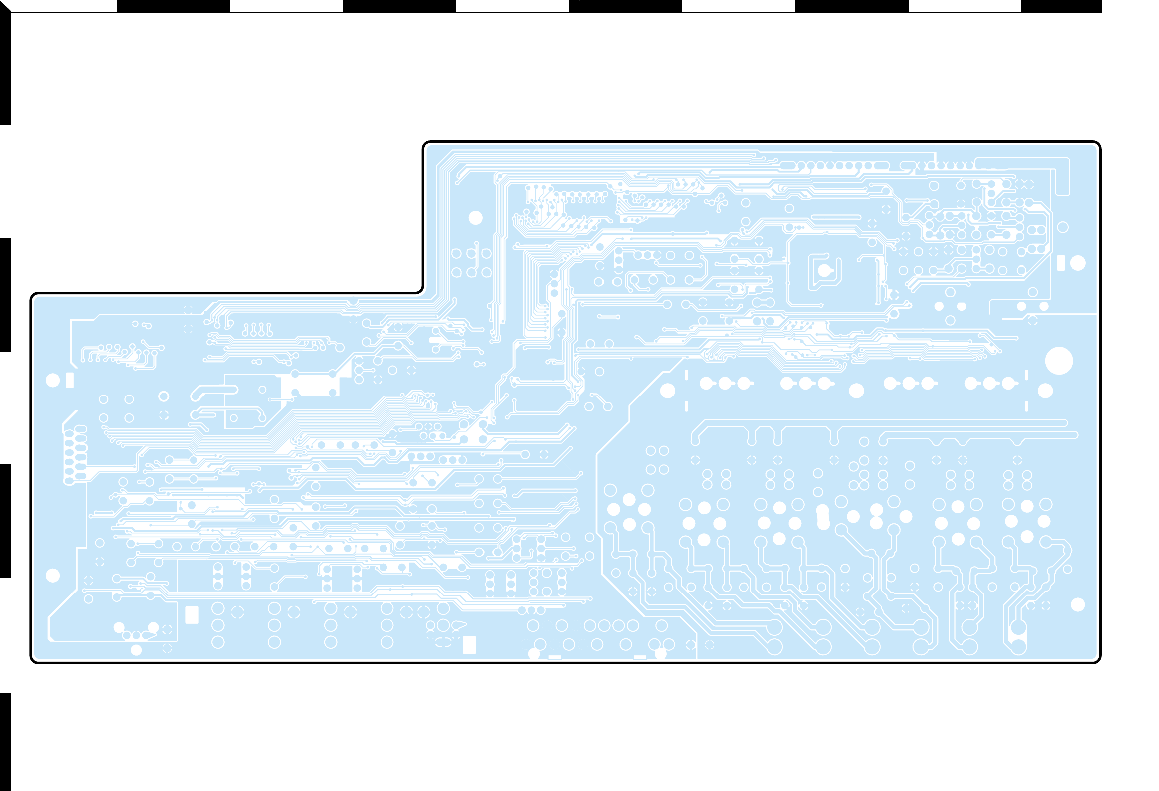
PC BOARD
(
Component side view
)
9 10
AJ AK AM AO AQ ASAL AN AP AR
2
1
3
5
7
4
6
MAIN
Refer to the schematic diagram for the value of resistors and capacitors.
PC BOARD
(
Foil side view
)
11 12
 Loading...