


GX-608EF2
© 2000-7 PRINTED IN JAPAN
B51-7638-00(S) 1889
SERVICE MANUAL
CD CASSETTE RECEIVER
GX-608EF2
POWER
TUNE/TRACK
REW
LOUD
FF
MUTE
SCN DISP
T. I NEWS
TONE/BAL
VOLUME
CD
BAND
CHR
TAPE
COMPACT
DIGITAL AUDIO
B NR REP RDM PROG
RELEASE
AUTO-REVERSE
DOLBY B NR
AME LOCAL
VOL ADJ REG
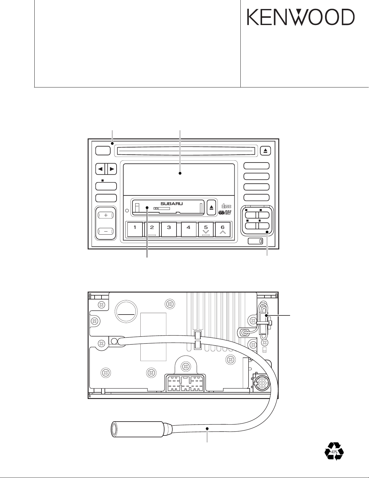
Front glass assy
(B10-3165-13)
Panel assy
(A64-2014-22)
TEL MUTE
A19
SUBAR U GENUINE
Sub panel assy
(A22-2807-13)
Cassette lid
(A53-1679-03)
Cord with plug (ANT)
(E30-4809-15)
Cord with connector
(Tel mute)
(E30-4810-05)
GX-608EF2
2
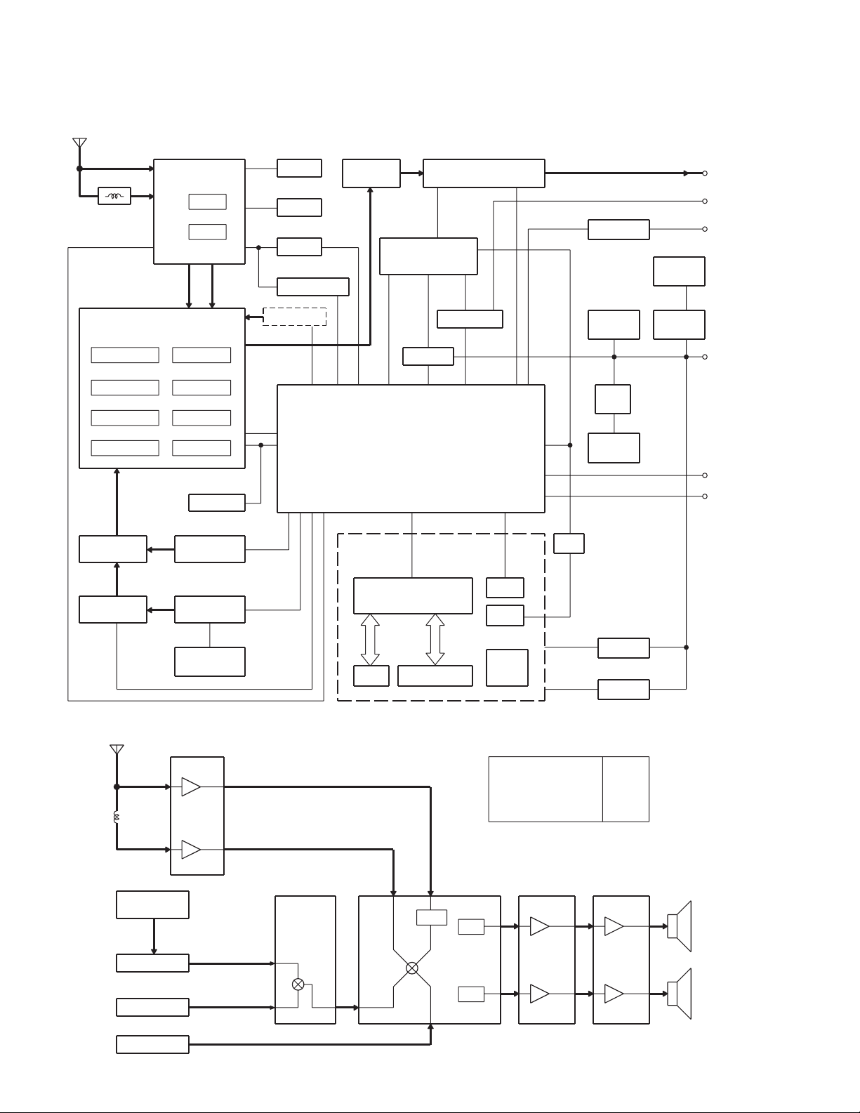
BLOCK DIAGRAM
L12
FM:223mV
AM:180mV
FM
AM
TAPE:345mV
CD:1200mV
CH:1200mV
0dB
0dB
0dB
AM:
FM:
TAPE:
CD:
CH:
-6.0dB
-9.0dB
-12.0dB
0.0dB
0.0dB
315Hz 0dB
1kHz 40kHzdev.
400Hz 30%mod.
1kHz 0dB
1kHz 0dB
F/E
ANT
SW AMP
IC21
FM
AM
EQ-DOLBY
CD-MECHA
CD-CH
IC22
E-VOL
-12dB
-12dB
IC31,32
FIX EQ
+34dB
+34dB
IC41
REAR
SP
SP
FRONT
MPX
AN7550NZNJM2060M
ATT
ATT
TDA7400D
BA3129F
0dB
CASSETTE
MECHA
ANT
F/E
IF/NC
PLL
FM+B
AM+B
A11 Q101
Q103
RDS
NOISE AMP
IC12
IC13
LOUD
BASS
TREBLE
ATT
FADER
ISO-AMP
SELECTOR
MPX
IC22
E-VOL
SW AMP
EQ,DOLBY
IC21
IC1 (D40-1079-05)
MECHA
(X92-3590-01)
CD MECHA
CASSETTE
FIX-EQ
IC31,32
IC81
EEPROM
IC84
CHANGER
SYSTEM u-COM
DRIVER
MOTOR
POWER IC
IC41
SP-OUT
MUTE Dr
IC83
Q709
BU DET.
Q904
ACC DET.
ACC
P-ANTANT-CON
Q94
PANEL u-COM
IC1
VFD KEY MATRIX
LAMP
(X25)
TDF
RST
RST
IC92
MECHA
Q701
AVR
A8V
AVR
Q704
AVR
VREF
IC72
BU5V
AVR
Q706
BACK UP
Q708
PON5V
SW
LAMP
A61
Q605,606
SMALL IN
TEL MUTE
DC/DC
Level difference of each sauce
GX-608EF2
3
●SYNTHESIZER UNIT(X14-6212-70)
Ref.No. Component Name Application/Function Operation/Condition/Compatibility
IC1 HA12216FP Dolby B
Playback EQ, Dolby B, blank space detection
IC2 BA6219BFP-Y Motor driver For cassette mechanism
IC12 NJM4565M-TE2 Operational amplifier For RDS noise amplifier
IC13 TDA7479D RDS decoder For RDS decoding
IC21 BA3129F SW operational amplifier For CD/TAPE switching
IC22 TDA7400D Electronic control BASS, TRE, MPX, EVOL
IC31,32 NJM2060M Operational amplifier For FIX-EQ
IC41 AN7550NZ Power amplifier 4-channel 35W power amplifier
IC71 M5237ML AVR control For AUDIO +8V power supply
IC72 NJM4580MD Operational amplifier 1/2 VCC output
IC81 UPD784216GF526 System microprocessor System control
IC82 PST9130NR Reset IC Reset detection
IC83 TC74HC02AF NOR circuit (4) For hard muting
IC84 BR24C01AF EEP-ROM For memory backup
Q1 2SB1443
Cassette mechanism main motor power switch
For cassette mechanism main motor
Q2 DTC114EK
Cassette mechanism main motor power switch
Pch-SW
Q3 DTC144EK Gain switching during tape searching Pch-SW, on during tape playback
Q4 DTA144EK Gain switching during tape searching Nch-SW, on during tape playback
Q5 DTC144EK Motor driver power switch Pch-SW
Q6 DTA114EK Motor driver power switch Nch-SW
Q7 2SB1443 Motor driver power supply For cassette mechanism submotor driver
Q8 2SC2412K(S) Motor driver power supply control For cassette mechanism submotor driver
Q9 DTC144EK Kick switch
On for emergency eject when submotor locked
Q101 2SB1188(Q,R) FM power switch For FM 8V
Q102 DTC124EK FM power switch Pch-SW
Q103 2SB1188(Q,R) AM power switch For AM 8V
Q104 DTC124EK AM power switch Pch-SW
Q107 DTC124EK IF mode forced switching switch Lo output at WIDE
Q108 2SC2412K(S) Noise amplifier Noise detection output buffer
Q109 DTC114TK Noise amplifier Constant switching when noise detected
Q110 DTA124EK Noise amplifier Constant switching when noise detected
Q201 DTC114EK Source switch switching Lo output at TAPE
Q202 2SA1037K Mute switch For CD muting
Q203 DTC144EK Mute switch For IC II 3 hard muting
Q204 DTC343TK Mute switch For CD muting, Rch
Q205 DTC343TK Mute switch For CD muting, Lch
Q601 DTC124EK DC/DC AVR switch Pch-SW
Q602 DTA124EK DC/DC AVR switch Nch-SW
Q603 2SB1184 DC/DC AVR For 13V AR
Q604 2SC2412K(S) DC/DC AVR control For 13V AR
Q605 2SB1565(E,F) Lamp AVR For 10V AR
Q606 2SB1565(E,F) Lamp AVR For 10V AR
Q607 DTA124EK Lamp AVR switch Nch-SW
Q608 2SC2412K(S) Lamp AVR control For 10V AR
Q609 DTC144EK Small detection Lo output at small ON
COMPONENT DESCRIPTION
GX-608EF2
4
●SWITCH UNIT(X25-8502-70)
Ref.No. Component Name Application/Function Operation/Condition/Compatibility
IC1 UPD78011FGC599 Display control microprocessor VFD control, key take in
Q1 DTC114EK 5V control Nch-SW
Q2 DTA114YK VFD power switch Pch-SW
Q3 DTC114YK 5V control VFD protection SW
Q4 DTC114EK VFD control VFD control
COMPONENT DESCRIPTION
Ref.No. Component Name Application/Function Operation/Condition/Compatibility
Q610 DTC114EK Lamp AVR switch P-CH-SW
Q701 2SB1565(E,F) CD mechanism AVR For 7.5V AVR
Q702 2SC2412K(S) CD mechanism AVR control For 7.5V AVR
Q703 DTA124EK CD mechanism AVR switch For 7.5V AVR
Q704 2SB1565(E,F) AVR For 8V AVR
Q705 DTA124EK AVR switch For 8V AVR
Q706 2SB1565(E,F) Microprocessor AVR For 5.6V AVR
Q707 2SC2412K(S) Microprocessor AVR control For 5.6V AVR
Q708 2SA1037K P-ON 5V switch P-ON 5V SW
Q709 2SC2412K(S) BU detection Lo output at BU ON
Q802 DTA114EK DSI control Hi output when DSI lit
Q803 DTC144EK AVR control switch On when P-ON 5V on
Q901 2SA1037K P-ANT circuit protection Antenna short-circuiting protection
Q902 DTA124EK P-ANT circuit protection Antenna short-circuiting protection
Q903 DTC144EK P-ANT circuit control switch P-ANT circuit control
Q94 2SB1443 P-ANT circuit control switch P-ANT circuit control
Q904 2SC2412K(S) ACC detection Lo output at ACC ON
GX-608EF2
5
SYSTEM MICROCOMPUTER : UPD784216GF526 (IC81 : X14-6212-70)
●Terminal Description
Pin Function I/O Description
1 AM+B O AM power output
2 FM+B O FM power output
3 P_MUTE O Power IC mute
4 P_STBY O Power IC standby
5 CD_SW3 I CD mechanism SW3
6 CD_MOTOR O CD mechanism loading motor
7 CD_LO/EJ I/O CD mechanism load/eject control
8 CD_MSTOP O CD mechanism mechanism stop
9 VDD -
10-23 CD_MRST O CD mechanism mechanism reset
11 CD_MUTE_L I Mute request from CD mechanism
(Lch)
12 BEEP O Beep output
13 CD_MDET I CD mechanism detection
14 CD_DATA_P I/O CD mechanism data line
15 CD_CLK O CD mechanism clock line
16 NC -
17 CD_MUTE_R I Mute request from CD mechanism
(Rch)
18 NC -
19 NC -
20 REF_CONT O A/D reference voltage control
21 CH_REQH I Communications request from
CDCH CH
22 TEST -
23 TYPE1 I Tuner setting 1
24 TYPE2 I Tuner setting 2
25 CD_SW1 I CD mechanism SW1
26 CD_SW2 I CD mechanism SW2
27 MUTE O Audio mute
28 P_ON O Peripheral power control
29 CH_ON O CDCH control output
30 CH_RST O CDCH reset
31 CH_MUTE I CDCH mute
32 ANT_CON O Antenna control
33 DC/DC O DC/DC
34 PACK_DET I
Cassette mechanism back detection
35 CS_STBY I Cassette mechanism standby
position detection
36 M_MOTOR O Cassette mechanism main motor
control
37 VDD -
38 X2 -
39 X1 -
40 VSS -
41 XT2 -
42 XT1 -
43 RESET I
44 BU_DET I BU detection
45 CD_SREQ I CD mechanism SIO
communications request
46 ACC_DET I ACC detection
47 ILLM_OUT O Illumination control
48 CH_REQC O Communications request from
CDCH CH
49 SC_REQ I
Communications request from panel
MICROCOMPUTER'S TERMINAL DESCRIPTION
Pin Function I/O Description
50 R_CLK I RDS CLK
51 AVDD -
52 AVREFO -
53 SMALL I SMAALL input
54 PHONE I Telephone detection
55 REEL_S I
Cassette mechanism reel pulse input
56 REEL_T I
Cassette mechanism reel pulse input
57 NC -
58 NOISE I Noise level
59 SMETER I S-meter level
60 MODE I
Cassette mechanism mechanism
position mode pulse input
61 AVSS -
62 SC_CON O Panel control output
63 SC_BUSY I Panel busy input
64 AVREF1 -
65 CH_DATAC I CDCH SIO input
66 CH_DATAH O CDCH SIO output
67 CH_CLK O CDCH SIO CLK
68 SC_DATA I CDCH SIO input
69 MC_DATA O CDCH SIO output
70 MC_CLK O CDCH SIO CLK
71 MC_REQ O Communications request to panel
72 NC -
73 PLL_CE O PLL SIO CE
74 PLL_DATA O PLL SIO output
75 PLL_CLK O PLL S10 CLK
76 DSI O Security LED control
77 TDF I Panel detach detection
78 SUB_P O
Cassette mechanism submotor control
79 SUB_M O
Cassette mechanism submotor control
80 KICK O Cassette mechanism kick control
81 R_DATA I RDS data
82 QUAL I RDS quality
83 PACK_IN I
Cassette mechanism tape insertion
detection
84 MUSIC O Cassette mechanism blank space
detection
85 MSGV O
Gain switching during tape search on
Cassette mechanism
86 F/R O
Cassette mechanism F/R switching
87 METAL I
Cassette mechanism metal detection
88 DOLBY O
Cassette mechanism Dolby switching
89 EQ_MUTE O Cassette mechanism EQ mute
90 NC -
91 NC -
92 AFC I AFC
93 IF_MODE O K21 IF status detection
94 WIDE O K21 control wide
95 NARROW O 21 control narrow
96 FM_SD I SD
97 SDA_IC2 I/O IC2 SDA
98 SCK_IC2 O IC2 SCK
99 A_SEL O Audio select
100 VSS -
GX-608EF2
6
Pin Function I/O Description
1 SC_BUSY O SYSCON panel busy output
2-8 NC -
9 VSS -
10,11 NC -
12-14 KR2-KR4 I Key read line
15-18 NC -
19-23 KS0-KS4 O Key scan line
24 VSS -
25-33 NC -
34 SC_REQ O Communications request to
SYSCON
35 RESET -
36 MC_REQ I Communications request from
SYSCON
37 KR1 I Key read line
38 KR0 I Key read line
39 SC_CON I SYSCON panel control
40 VDD -
41 X2 -
42 X1 -
43 IC -
44 XT2 -
45 NC -
46 AVSS -
47-54 NC -
55 AVDD -
56 AVREF -
57 VFD_ON O VFD power control
58 VFD_DATA O VFD SIO output
59 VFD_CLK O VFD SIOclock
60 VFD_LAT O VFD SIO latch
61 VFD_BLK O VFD blanking
62 MC_DATA I SYSCON SIO input
63 SC_DATA O SYSCON SIO output
64 MC_CLK I SYSCON SIO clock
MICROCOMPUTER'S TERMINAL DESCRIPTION
PANEL MICROCOMPUTER : UPD78011FGC599 (IC1 : X25-8502-70)
●Terminal Description
GX-608EF2
7
Pin Function I/O Description Processing Operation
1 BDO I Dropout signal input H: detected (Photodetector signal input 1)
2 OFT I Off track signal input H: detected (Photodetector signal input 2)
3 /RFDET I RF detection signal input H: detected (Photodetector signal input 3)
4 VDET I Vibration detection signal input H: detected (Photodetector signal input 4)
5 LDON O Laser on signal output H: ON (Photodetector RF signal adding input)
6 NC - No connection (RF amplifier filter terminal 1)
7 NC - No connection (RF amplifier filter terminal 2)
8 AVSS3 I Analog circuit GND
9 AVDD3 I Analog circuit power supply
10 FBAL O Focus balance adjustment output Laser diode monitor input
11 TBAL O Tracking balance adjustment output Laser diode drive output
12 FE I Focus error signal input (DA input)
13 NC - No connection (Tracking filter filter terminal 1)
14 NC - No connection (Tracking filter filter terminal 1)
15 TE I Tracking error signal input (analog input)
16 NC - No connection (Track cross comparator filter terminal)
17 NC - No connection
18 NC - No connection RF signal input (for RF detection)
19 RFENV I RF envelop signal input
20 VREF I VREF input terminal
21 ARF I RF signal input (for DSL)
22 DRF I DSL bias terminal
23 DSLF I/O DSL loop filter terminal
24 IREF I Reference voltage input terminal
25 PLLF I/O PLL loop filter terminal
26 PLFF2 I/O PLL loop filter properties switching terminal
27 VCOF I/O VCO loop filter terminal
28 VCOF2 I/O Digital servo 33.8688 MHz generating
VCO loop filter terminal
29 TRV O Traverse forced feeding output
30 TVD O Traverse drive output
31 PC O Spindle motor on detection L: ON
32 ECM O Spindle motor drive output (forced mode output)
(DA output)
33 ECS O Spindle motor drive output
(Servo error signal output)
34 KICK O Kick pulse output
35 TRD O Tracking drive output
36 FOD O Focus drive output
37 TOFS O Tracking offset adjustment output
38 AVDD2 I Analog circuit power supply
(for DSL, PLL, AD and DA sections)
39 AVSS2 I Analog circuit GND
(for DSL, PLL, AD and DA sections)
40 DVSS2 I Digital circuit GND
41 EFM or CK384 O EFM signal output Default : EFM signal output
When command executed : 16.9344 MHz clock
output
42 PCK or DSLB O PLL sampling clock output Default : PLL sampling clock output
When command executed : DSL balance output
43 /CLDCK O Subcode frame clock signal output
44 FCLK O Crystal frame clock signal output
45 IPFLAG O Interpolation flag signal output H: interpolation
46 FLAG O Flag signal output
47 TRCRS O Track cross signal input (Track cross signal output)
MICROCOMPUTER'S TERMINAL DESCRIPTION
MECHANISM MICROCOMPUTER : MN662770KA7 (IC2 : X32-4600-00)
●Terminal Description
GX-608EF2
8
Pin Function I/O Description Processing Operation
48 STOUT O Monitor signal serial data output
(OFT, VDET, BDO, RFDET, etc.)
49 STLD O Monitor signal load signal output
50 SMCK O Monitor signal bit lock signal output
51 CSEL I Crystal oscillator frequency setting terminal L: locked
H: 33.8688 MHz L: 16.9344 MHz
52 TEST1 I Test terminal 1 L: locked (normal)
53 TEST2 I Test terminal 2 L: locked (normal)
54 IOSEL I Audio DAC external data input mode setting
terminal
55 /NRST I Reset input L: reset
56 BCLK O SRDATA bit clock output
57 LRCK O L/R identification signal output
58 SRDATA O Serial data output
59 SUBC O Subcode serial output
60 SBCK I Subcode serial output clock input
61 DQSY O CD-TEXT read enable signal output
62 DEMPH O Deemphasis detection signal input L: ON
63 TX O Digital audio interface signal output
64 SRDATAIN I SRDATA input/test terminal
65 LRCKIN I LRCK input/SMCK output frequency switching
66 BCLKIN I BCLK input When not used: VDD
67 DVDD1 I Digital circuit power supply
68 X1 I Crystal oscillator circuit input terminal
69 X2 O Crystal oscillator circuit output terminal
70 DVSS1 I Digital circuit GND
71 XSUB1 I Microprocessor clock input terminal
72 XSUB2 O Microprocessor clock output terminal
73 DVDD2 I Digital circuit power supply
74-78 NC O No connection
79 CLVS O
Spindle servo phase synchronization signal output
H = CLV L = rough servo
80 TEST I Test mode switching terminal
81 ASEL I Audio output polarity detection terminal
82 PON O Audio and digital power supply control terminal
83 SEARCH O Servo IC gain switching control terminal
84 VER/HOR O Vertical/horizontal installation switching monitor
terminal
85 SW3 I Limit switch detection terminal
86 /MUTE_L O Lch analog mute control terminal
87 /MUTE_R O Rch analog mute control terminal
88 CD_R O CD-R control terminal
89 /RST I System reset input terminal
90 NC I No connection
91 /MSTOP I Standby detection terminal
92 NC O No connection
93 DATA I/O 12C bus data line
(communications line with system microprocessor)
94 /CLK I/O 12C bus clock line
(communications line with system microprocessor)
95 HOT I Temperature protection detection terminal
96 VREF+ I A/D converter power supply
97 OUTR O Rch audio output
98 AVDD1 I Analog circuit power supply
(for audio output section (both Lch and Rch))
99 OUTL O Lch audio output
100 AVSS1 I Analog circuit GND
MICROCOMPUTER'S TERMINAL DESCRIPTION
 Loading...