


 Loading...
2DIN CD RECEIVER
DPX501/501U/501UY DPX-MP2090U
SERVICE MANUAL
© 2006-4 PRINTED IN JAPAN B53-0400-00 (N) 960
DPX501 (K type) |
|
Panel assy (A64-3814-02) |
DPX501U/501UY (E type) |
|
Panel assy (A64-3871-02) |
|||||||
|
|
|
|
|
DPX501 |
|
|
|
|
DPX501U |
||
|
|
|
|
|
|
|
|
|
|
|
System |
EX |
|
|
|
|
|
FM |
SCRL |
|
|
|
|
FM |
SCRL |
|
|
EXTERNAL MEDIA CONTROL |
|
|
|
|
|
EXTERNAL MEDIA CONTROL |
|
|||
|
AUTO |
|
|
|
AM |
SW |
|
TI |
|
|
AM |
SW |
|
|
|
|
|
|
|
|
|
||||
|
AME |
MENU |
|
OFF |
|
|
|
AME |
MENU |
|
OFF |
/PTY |
|
|
PTY/C.S. |
|
|
|
|||||||
VOL |
S.MODE SCAN |
RDM A.RDM |
REP |
F.SEL M.RDM |
|
|
VOL |
S.MODE SCAN |
RDM A.RDM |
REP |
F.SEL M.RDM |
|
ATT |
AUD |
|
|
|
USB |
ATT |
AUD |
|
|
USB |
||
SET UP |
|
|
|
SET UP |
|
|
||||||
DPX-MP2090U (M type) |
Panel assy (A64-3966-02) |
|
|
|
|
|
|
|||||
|
|
|
|
|
|
|
|
Lever (K,E type) |
Antenna adaptor (E type) |
|||
|
|
|
|
|
|
|
|
(D10-4589-04) x2 |
(T90-0523-05) |
|
||
|
|
|
|
|
DPX-MP2090U |
|
|
|
|
|
|
|
|
|
|
|
|
|
System |
EX |
|
|
|
|
|
|
FM |
SCRL |
|
|
|
EXTERNAL MEDIA CONTROL |
|
|
|
|
|
|
AUTO |
|
|
|
AM |
SW |
|
|
|
|
|
|
||
|
|
AME |
MENU |
|
|
OFF |
|
VOL |
S.MODE |
SCAN |
RDM A.RDM |
REP |
F.SEL |
M.RDM |
|
ATT |
AUD |
|
|
|
|
USB |
|
SET UP |
|
|
|
|
|||
Screw set (K,M type) |
Adhesive double- |
(N99-1779-05) |
coated tape (K,E type) |
|
(H30-0595-04) |
DC cord |
DC cord (E type) |
Cord with connector(USB) |
(E30-6408-05):(M type) |
(E30-6412-05) |
(E30-6535-05) |
(E30-6414-05):(K type) |
|
|
1.5m
Remote controller assy (K,M type) (A70-2067-15)
SIZE AA BATTERY(K,M type) (Not supplied)
RC-527
Escutcheon (K,E type) |
Escutcheon (M type) |
Escutcheon (K,E type) |
Mounting hardware |
Compact disc |
(B07-3172-12) |
(B07-3046-04) |
(B07-3165-02) |
assy (K,E type) |
(W01-1673-05):(K,M type) |
|
|
|
(J22-0429-13) |
(W01-1674-05):(E type) |
This product uses Lead Free solder.
DPX501/501U/501UY DPX-MP2090U
BLOCK DIAGRAM
● Complete view
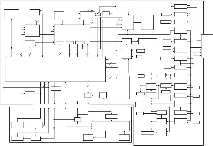
ELECTRIC UNIT (X34- )
CN5 |
|
IC9 |
|
|
|
|
|
BU5V |
D5V |
|
|
PON USB/C DET |
|
|
|
CN4 |
|
|
|
DME1 |
|
CN2,3 |
|
|
|
||
OPEL DISP |
|
SW5 |
|
|
|
|
|
|
BU |
||||
RDS |
|
|
|
A8V |
|
|
2 |
|
|
||||
|
|
|
|
|
|
|
USB5 IC4 |
||||||
MARINE RC |
|
|
AUX IN |
|
|
CD MECHA |
USB |
|
|||||
OEM RC |
|
|
|
|
SERVO+B |
|
|
|
|
||||
|
W1 |
|
|
|
|
|
|
|
3 |
|
|||
|
|
|
|
|
|
|
|
|
|
||||
|
|
A1 |
|
IC2 |
|
|
|
|
2 |
|
|
1 |
PW-IC |
|
|
|
|
|
|
|
|
|
|
|
|||
|
TUN8V |
F/E |
A8V |
|
|
|
|
|
|
|
|
|
|
|
SW5 |
PRE+B |
|
|
|
|
|
|
|
|
|
|
|
|
AM+B |
FST |
PREF |
|
|
E-VOL |
|
|
|
|
|
|
|
|
|
|
|
|
|
|
|
|
|
|
|
||
|
|
J2 |
|
|
|
|
|
|
|
|
|
|
Q400-405 |
|
|
|
|
|
|
|
|
|
|
|
|
MUTE |
|
|
|
LX-BUS |
|
MUTE |
|
MUTE |
DC-DET |
|
|
|
|
||
|
|
|
|
|
|
|
|
|
|||||
|
|
|
|
|
|
|
|
|
|
|
|
|
|
|
|
BU |
|
|
|
|
|
1 |
|
|
|
|
IC6 |
|
|
|
|
|
|
|
|
|
|
|
|
||
3 |
7 |
8 |
|
1 |
|
3 |
1 |
3 |
|
10 |
|
|
MUTE |
IC1 |
|
|
|
|
|
|
|
|
|
|
|
|
LOGIC |
|
|
|
|
|
|
|
|
|
|
|
BU5 |
|
|
|
|
|
|
|
|
|
|
|
|
|
1 |
|
BU5 |
|
|
|
|
|
|
|
|
|
|
|
|
|
|
|
|
|
|
|
|
|
|
|
|
|
1 |
|
|
|
|
|
SYSTEM u-COM |
|
|
|
|
|
2 |
|
|
||
|
|
|
|
|
|
|
|
|
|
|
|
|
|
|
|
|
|
|
|
|
|
|
|
|
9 |
DC-CN etc |
|
|
|
|
|
|
|
|
|
|
|
|
|
||
|
|
|
|
|
|
|
|
|
|
|
|
PHONE |
|
|
|
|
|
|
|
|
|
|
|
|
|
DIMMER/ |
|
|
|
|
2 |
Q13 |
5 |
|
|
1 |
|
|
|
ACC DET |
|
|
|
|
|
|
|
|
|
BU DET/ |
|||||
|
|
|
|
|
|
|
|
|
|
|
|
||
|
|
IC7 |
|
PAN5V |
|
|
|
|
|
|
|
ANT CON |
|
|
|
|
|
|
|
ILLUMI+B |
|
IC13 |
|
|
P CON/P ON |
||
|
BU5 |
RESET |
|
|
|
|
|
|
|
P ON CD/ |
|||
|
|
BU5 |
|
|
|
FL+B |
3/4W |
|
P ON ILLUMI |
||||
|
|
|
|
|
|
|
Rx10 |
|
P ON FL/ |
||||
|
|
|
|
|
|
|
|
|
|
|
EX-AMP |
||
|
|
|
|
|
|
|
|
|
|
|
|
||
|
J4 |
|
|
|
|
|
|
CN |
|
|
|
|
|
|
J1 |
|
|
|
2DIN |
|
|
|
|
|
|
||
|
|
|
|
|
R73 |
|
|
|
|
|
|
1/2W Rx1 |
|
S3 |
S1 |
SW |
|
ED1 |
|
|
|
|
|
|
|||
RESET |
ROTARY |
|
|
|
VFD |
|
ENCODER |
|
|
|
|||
|
|
|
DRIVER & KEY MATRIX BUILT-IN,NEW |
|||
|
SW5 |
|
|
|
|
|
IC2 |
Q6 |
|
|
COLOR |
|
|
PAN5 |
KEY |
SELECT |
KEY |
|||
REMOTE |
SW5 |
|||||
SW5V |
|
ILLUMI |
|
MATRIX |
||
C104,D107,R112
|
PHONE |
PHONE |
BU5 |
|
|
|
|||
|
|
Q108 |
BU5 |
|
J1 |
DIMMER |
DIMMER |
||
SP-OUT |
|
Q112 |
|
|
|
|
|
||
FRONT L/R |
ACC DET |
ACC-DET |
|
|
|
|
|
||
REAR L/R |
|
Q109 |
|
|
NF L/R |
|
SURGE- |
|
|
|
|
|
||
|
|
DET |
J1 |
|
|
|
BU5 |
||
J3 |
|
DC-CN |
||
|
Q111 |
|||
PRE-OUT |
|
|
||
BU DET |
BU-DET |
PHONE |
||
FRONT/REAR/(NF) |
ILLUMI |
|||
|
|
|||
|
|
Q107 |
ACC |
|
Q111 |
EX-AMP |
EXT-AMP- |
B.U. |
|
|
|
EXT-CONT |
||
BU DET |
BU5 |
CON |
||
P-ANT |
||||
Q114 |
|
|||
|
Q101,102 |
|||
|
P-CON |
|||
RST |
|
|||
ANT CON |
ANT-CON |
|
||
|
|
|
|
|
Q103,106 |
|
|
|
|
P CON PCON-SW |
|
||
|
SW5 |
Q3,11 |
Q1,2 |
|
|
|
SW5V |
BU5V |
|
||
P ON |
|
||||
|
|
|
|||
|
BU5 |
|
|
|
|
|
IC8 |
IC12 |
Q12,21 |
|
|
USB5 |
HISIDE |
CD5V |
SURGE |
|
|
|
SW |
|
SW20V |
P ON |
|
C DET |
PON USB |
PON CD |
Q5,6,10 |
|
|
|
A8V |
|
|||
|
|
|
P ON |
||
|
D5V |
|
|
||
|
|
Q7,8 |
|
||
|
A8V |
|
|
||
|
|
CD |
|
||
SERVO+B |
|
|
|||
|
SERVO |
|
|||
|
|
|
|
||
|
AM+B |
Q300,301 |
Q4,9 |
|
|
AM+B |
AM+B |
SW14V |
P ON |
||
|
|||||
|
|
|
|||
|
Q302,303 |
IC5 |
|
||
|
TUN8V |
TUNER |
ILLUMI |
|
|
|
8V |
+B |
P ON |
||
|
|
||||
ILLUMI+B |
Q305,306 |
|
|
||
SW |
|
|
|||
PON ILLUMI |
ILLUMI |
|
|
||
+B |
|
|
|||
|
|
|
|
||
SWITCH UNIT (X16- )
2
DPX501/501U/501UY DPX-MP2090U
BLOCK DIAGRAM
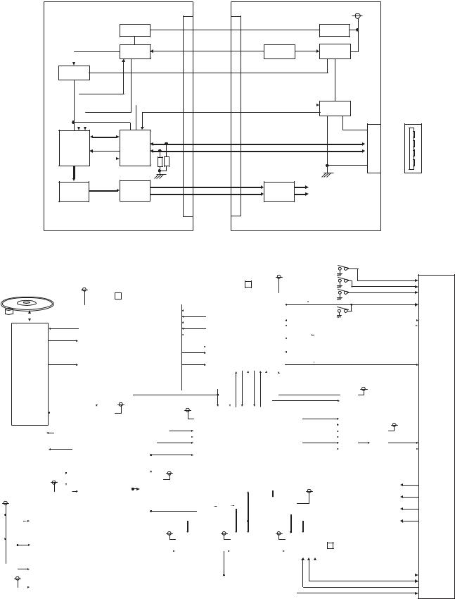
● AC Drive + USB Mechanism unit |
|
|
|
|
|
||
DXM-6810W/DXM-6820W |
CD_Mechanism |
30Pin FFC |
|
H/U |
|
|
|
|
|
|
CN1 |
|
|
BU14V |
|
|
|
|
|
|
|
|
|
|
IC19 |
BU5.0V |
|
|
|
|
|
|
|
BU3.3V |
|
|
BU5.0V |
|
|
|
|
|
|
|
|
||
|
IC1 |
|
|
|
5V |
|
|
|
P-ON |
Mecha- |
/MSTOP |
SYS- |
P-ON |
|
|
|
|
uCOM |
|
uCOM |
|
SW-Reg. |
|
IC20,21 |
|
|
|
|
|
|
|
CS3.3V |
|
|
D5.0V |
|
|
|
|
(CS1.8V) |
|
|
|
|
|
|
|
|
|
|
|
|
|
(VBUS 5V) |
|
|
|
|
PowerON SW |
|
|
High-side |
|
|
/CS RST |
|
|
|
|
|
|
|
|
Over Current |
|
|
Switch |
|
|
|
|
|
|
|
|
|
|
IC15 |
IC25 |
|
|
|
USB_5V |
|
|
|
|
USB |
USB_D+ |
|
|
USB_D+ |
|
DECODER |
/INT |
|
|
|
USB_D- |
Cable |
|
DRIVER |
|
|
|
||||
|
/RESET |
USB_D- |
|
|
|
|
|
|
|
|
|
|
|
||
|
|
|
|
|
|
USB GND |
|
IC18 |
IC13 |
|
|
|
|
|
|
|
|
|
L-ch |
|
|
|
|
DAC |
|
LFP |
|
EVOL |
|
|
|
|
|
|
R-ch |
|
|
|
|
USB CONNECTOR
● CD player unit (X32-583)
|
|
|
|
|
|
|
|
|
|
|
|
|
|
|
|
|
|
|
|
|
|
|
|
|
|
|
|
|
|
|
|
|
|
|
|
|
|
CS POWER |
|
|
|
|
|
|
|
|
|
|
|
|
|
|
|
|
|
|
|
||||||
|
|
|
|
|
|
|
|
|
|
|
|
|
|
|
|
|
|
|
|
|
|
|
|
|
|
|
|
|
|
|
|
|
|
|
|
|
POW ON |
|
|
|
|
|
|
|
11.500MHz |
|
|
BU3.3V |
|
|
|
|
|
|
|
||||||||
|
|
|
|
|
|
|
|
|
|
|
|
|
|
|
SW3.3V(712) |
|
16.893M |
|
|
|
|
|
|
|
|
|
|
|
|
|
|
|
|
|
|
|
|
|
|
|
|
|
|
|
|
|
|
|
|
|
|
|
|
|
|
||||||||
|
|
|
|
|
|
|
|
|
|
|
|
|
|
|
|
|
|
|
|
|
|
|
|
|
|
|
|
|
|
|
|
|
|
|
|
|
|
|
|
|
|
|
|
|
|
|
|
|
|
|
|
|
|
||||||||||
|
|
|
|
|
|
|
|
|
|
|
|
|
|
|
|
|
|
|
|
|
|
|
|
|
|
|
|
|
|
|
|
|
|
|
|
|
|
|
|
|
|
|
|
|
|
|
|
|
|
|
|
|
|
|
|
|
|
|
|||||
|
|
|
|
|
|
|
|
|
|
|
|
|
|
|
|
|
|
|
|
|
|
|
|
|
|
|
|
|
|
|
|
|
|
|
|
|
|
|
|
|
|
|
|
|
|
|
|
|
|
|
|
|
|
|
|
|
Q7 |
|
|
|
|
|
|
|
|
|
|
|
|
|
|
|
|
|
|
|
|
|
|
|
|
|
|
|
|
|
|
|
|
|
|
|
|
|
|
|
|
|
|
|
|
|
|
|
|
|
|
|
|
|
|
|
|
|
|
|
|
|
|
|
3.3 |
5V |
|
|
|
|
|
|
|
|
|
|
|
|
|
|
|
|
|
|
|
|
|
|
|
|
|
|
|
|
|
|
|
|
|
|
|
|
|
|
|
|
|
A0 |
|
|
|
|
|
|
|
|
|
|
|
|
|
|
|
|
|
(SW3.3V) |
|
|
|
|
|||||
|
|
|
|
|
|
|
|
|
|
|
|
|
|
|
|
|
|
|
|
|
|
|
|
|
|
|
|
|
|
|
|
|
|
|
|
|
|
|
|
|
|
|
|
|
|
|
|
|
|
|
|
|
|
|
|
|
|
|
|
||||
|
|
DPU1 |
|
|
|
|
|
|
|
|
|
|
|
|
|
|
|
|
|
|
|
|
|
|
|
|
|
|
SI |
|
|
|
|
|
|
|
|
|
|
|
|
|
|
|
|
|
|
|
|
|
|
|
|
||||||||||
|
|
|
|
|
|
|
|
|
|
|
|
|
|
|
|
|
|
|
|
|
|
|
|
|
|
|
STB |
|
|
|
|
|
|
|
|
|
|
|
|
|
|
|
|
|
|
|
|
|
|
|
|
||||||||||||
|
|
|
|
|
|
|
|
|
|
|
|
|
|
|
|
|
|
|
|
|
|
|
|
|
|
|
|
|
|
|
|
|
|
|
|
SCK |
|
|
|
|
|
|
|
|
|
|
|
|
|
|
|
|
|
|
Q6 |
|
|
|
|
|
|||
|
|
|
|
|
LD |
|
|
|
|
|
|
|
|
|
|
|
|
|
|
|
|
|
|
|
|
|
|
|
|
|
|
|
|
|
|
|
|
|
|
|
|
|
-COM |
|
|
|
|
|
|
|
|
|
|
|
|||||||||
|
|
|
|
|
|
|
|
|
|
|
|
|
|
|
|
|
|
|
|
|
|
|
|
|
|
|
|
|
|
|
|
|
/RESET |
|
|
|
|
|
|
|
|
|
|
|
|
|
|
|
|
|
|
|
|
||||||||||
|
|
|
|
|
|
|
|
|
|
|
|
|
|
|
|
|
|
|
|
|
|
|
|
|
|
|
|
|
|
|
|
|
|
|
|
|
|
|
|
|
|
|
|
|
|
|
|
|
|
|
|
|
|
|
|
|
|
3.3 |
5V |
|
|
|
|
|
|
|
|
|
PD |
|
|
|
|
|
|
|
|
|
|
|
|
|
|
|
RF AMP |
|
|
|
|
|
|
|
SO |
|
|
|
|
|
|
|
|
|
|
IC1 |
|
|
|
|
|
|
(BU5V ) |
|
|
|
|
||||||||||||
|
|
|
|
|
|
|
|
|
|
|
|
|
|
|
|
|
|
|
|
|
|
|
|
|
|
|
|
|
|
|
|
|
|
|
|
|
|
|
|
|
|
|
|
|
|
|
|
|
|
|
|||||||||||||
|
|
|
|
|
|
|
|
|
|
|
|
|
|
|
|
|
|
|
|
|
|
SERVO DSP |
|
|
|
|
|
|
INTQ |
|
|
|
|
|
|
|
|
|
|
|
|
|
|
|
|
|
|
|
|
|
|
||||||||||||
|
|
|
|
|
E |
|
|
|
|
|
|
|
|
|
|
|
|
|
|
|
|
|
|
|
|
|
|
|
|
|
|
|
|
|
|
|
|
|
|
|
|
|
|
|
|
|
|
|
|
|
|
|
|
|
|
|
Q3 |
|
|
|
|
|
|
|
|
|
|
|
|
|
|
|
|
|
|
|
|
|
|
|
|
|
|
|
|
|
|
|
|
IC2 |
|
|
|
|
|
|
DA_EMPH |
|
|
|
|
|
|
|
|
|
|
|
|
|
|
|
|
|
|
3.3 |
5V |
|
|
|
|
||||||
|
|
|
|
|
|
|
|
|
|
|
|
|
|
|
|
|
|
|
|
|
|
|
|
|
|
|
|
|
|
|
|
|
|
|
|
|
|
|
|
|
|
|
|
|
|
|
|
||||||||||||||||
|
|
|
|
A |
B |
|
|
|
|
|
|
|
|
|
|
|
|
|
|
|
|
|
|
|
|
|
|
|
|
|
|
|
|
|
|
|
|
|
|
|
|
|
|
|
|
|
|
|
|
|
|
|
|
|
|
|
(BU5V) |
|
|
|
|
||
|
|
|
|
|
C |
|
|
|
|
|
|
|
|
|
|
|
|
|
|
|
|
|
|
|
|
|
|
|
|
|
|
|
|
|
|
|
|
|
|
/CSRST |
|
|
|
|
MUTDATA DATS |
|
|
|
|
|
|
|
|
|
|
|
|
|
|
|
|
||
|
|
|
|
|
|
|
|
|
|
|
|
|
|
|
|
|
|
|
|
|
|
|
S7.5V |
|
|
|
|
|
I2S |
|
CS3.3V & |
|
|
|
|
|
|
DATB CLK SREQ BREQ EMPHCS |
|
|
|
|
|
|
|
EMPH |
|||||||||||||||||
|
|
|
|
|
|
|
|
|
|
|
|
|
|
|
|
|
|
|
|
|
|
|
|
|
|
|
|
|
|
|
|
|
|
|
|
|
|
|
|
|
|
|
|
|
|
|
|
|
|
|
|
|
|
|
|
|
|
|
|
|
|||
|
|
|
|
|
F |
|
|
|
|
|
|
|
|
|
|
|
|
|
|
|
|
|
|
|
|
|
|
|
|
|
|
|
|
|
|
|
|
|
|
|
delay |
|
|
|
|
|
|
|
|
|
|
|
|
Infinity 0 Det. |
|||||||||
|
|
|
|
|
|
|
|
|
|
|
|
|
|
|
|
|
|
|
|
|
|
|
|
|
|
|
|
|
|
|
|
|
|
|
|
|
|
|
|
|
|
|
|
|
|
|
|
|
|
|
|
|
|
|
|
||||||||
|
|
|
|
TR COIL |
|
|
|
|
|
|
|
|
|
|
IC4 |
|
|
|
|
|
|
|
|
|
|
|
|
|
|
|
CS1.8V |
|
|
|
|
|
|
|
|
|
|
|
|
|
|
|
|
|
|
DAC_RST |
|||||||||||||
|
|
|
|
|
|
|
|
|
|
|
|
|
|
|
|
|
|
|
|
|
|
|
|
|
|
|
|
|
|
|
|
|
|
|
|
|
|
|
|
|
|
|
|
|
|
|
|
|
|
|
|
|
|
|
|
|
|
||||||
|
|
|
|
|
|
|
|
|
|
|
|
|
|
|
|
|
|
|
|
|
|
|
|
|
|
|
|
|
|
|
|
|
|
|
|
|
|
|
|
|
|
|
|
|
|
|
|
|
|
|
|
|
|
|
|
|
|
||||||
|
|
|
|
|
|
|
|
|
|
|
|
|
|
|
|
|
|
|
|
|
|
|
|
|
|
|
|
|
|
|
|
|
|
|
|
|
|
|
|
|
|
|
|
|
|
|
|
|
|
|
|
|
|
|
|
|
|
||||||
|
|
|
|
FO COIL |
|
|
|
|
|
|
|
|
|
|
|
Motor |
|
|
|
|
|
|
|
|
|
|
|
|
|
|
|
|
|
|
|
|
|
|
|
|
|
|
|
|
|
SER2(3/4Wire) |
|
|
|
|
|
|
|||||||||||
|
|
|
|
|
|
|
|
|
|
|
|
|
|
|
|
|
|
|
|
|
|
|
|
|
|
|
|
|
|
|
|
|
|
|
|
|
|
|
|
|
|
|
|
|
|
|
|
|
|
|
|
|
|
|
|
DAC_MUTE |
|||||||
|
|
|
|
|
|
|
|
|
|
|
|
|
|
|
|
|
|
Driver |
|
|
|
|
|
|
|
|
|
|
|
|
|
|
DATA |
|
|
|
|
|
|
|
|
|
|
|
|
|
|
|
|
|
|
|
|
PCM_XCK |
|||||||||
|
|
|
SP MOTOR |
|
|
|
|
|
|
|
|
|
|
|
|
|
|
|
|
|
|
|
|
|
|
|
|
|
LRCK |
|
CD I/F |
|
|
|
|
ACD DECODER |
|
PCM_DATA |
|||||||||||||||||||||||||
|
|
|
|
|
|
|
|
|
|
|
|
|
|
|
|
|
|
|
|
|
|
|
|
|
|
|
|
|
|
|
|
|
|
BCLK |
|
|
|
|
|
|
|
|
|
PCM_LRCK |
|||||||||||||||||||
|
|
Loading & sled |
|
|
|
|
|
|
|
|
|
|
|
|
|
|
|
|
|
|
|
|
|
|
|
|
|
|
|
|
|
|
|
|
|
|
|
|
MP3/WMA/AAC |
|
PCM_BCLK |
||||||||||||||||||||||
|
|
MOTOR |
|
|
|
|
|
|
|
|
|
|
|
|
|
|
|
|
|
|
|
|
|
|
|
|
C16 |
|
|
|
|
|
|
|
|
DECODER |
|
|
|
|
|
|
|
|
|
|
|
|
|||||||||||||||
|
|
|
|
|
|
|
|
|
|
|
|
|
|
|
|
|
|
|
|
|
|
|
|
|
|
|
PLL |
|
|
|
|
|
|
|
|
|
|
|
|
|
|
|
|
||||||||||||||||||||
|
|
|
|
|
CS POW |
|
|
|
|
|
|
|
|
|
|
|
|
|
|
|
|
|
|
|
|
CS3.3V |
|
|
|
|
|
|
|
|
|
|
|
|
IC15 |
|
|
|
|
|
|
|
|
|
|
|
|
||||||||||||
|
|
|
|
|
|
|
|
|
|
|
|
|
|
|
|
|
|
|
|
|
|
|
|
|
|
|
|
|
|
|
|
|
|
|
|
|
|
|
|
|
|
|
|
|
|
|
|
|
|
|
|
||||||||||||
|
|
|
|
|
|
|
|
|
|
|
|
|
|
|
|
|
|
|
|
|
IC28 |
|
(CS7410) |
|
|
|
|
|
|
|
|
|
|
|
|
|
|
|
|
|
|
|
|
|
|
|
|
|
|
|
|||||||||||||
|
|
|
|
|
POWER |
|
|
|
|
|
|
|
|
|
|
|
|
|
|
|
|
|
|
|
|
|
|
|
|
|
|
|
|
|
|
|
|
|
|
|
|
Memory |
|
|
|
|
|
|
|
|
|
|
|
|
|||||||||
|
|
|
|
|
|
|
|
|
A8V |
|
|
|
|
|
|
IC14 SW A5V |
|
|
|
|
|
|
|
|
|
|
|
|
|
|
|
|
|
|
|
|
|
|
|
|
|
|
|
|
|
|
|
|
|
|
|
|
|||||||||||
|
|
|
|
|
|
|
|
|
|
|
|
|
|
|
|
|
|
|
|
|
|
|
|
|
|
|
|
|
|
|
|
|
|
|
|
|
|
|
Controller |
|
|
|
|
|
|
|
|
|
|
|
|
||||||||||||
|
|
|
|
|
|
|
|
|
|
|
|
|
|
|
|
|
|
|
3STATE |
|
|
|
|
|
|
|
|
|
|
|
|
|
|
|
|
|
|
|
|
|
|
|
|
|
|
|
|
|
|
||||||||||||||
|
|
|
|
|
|
|
|
|
|
|
SW |
|
|
|
5V Reg. |
|
|
|
|
|
|
|
|
|
BUFFER |
|
|
|
|
|
|
|
|
|
|
|
|
|
|
|
|
|
|
|
|
|
|
|
|
|
|
|
CS3.3V |
||||||||||
|
|
|
|
|
|
|
|
|
|
|
|
|
|
|
|
|
|
|
|
|
|
|
|
|
|
|
|
|
|
|
|
|
|
|
|
|
|
|
|
|
|
|
|
|
|
|
|
|
|
||||||||||||||
D5V(D4V) |
|
|
|
|
|
|
|
|
|
|
|
|
|
|
|
|
|
|
|
|
|
|
|
|
DRAM |
|
ROM |
|
|
/CS , A20 |
|
|
(CS7410) |
||||||||||||||||||||||||||||||
|
|
|
|
|
|
|
|
|
|
|
|
|
|
|
|
|
|
|
|
|
|
|
|
|
|
|
|
|
|
|
|
|
|
|
|
|
|
|
|
|
|
|
|
|
|
||||||||||||||||||
|
|
|
|
|
|
|
|
|
|
|
|
|
|
|
|
|
|
|
|
|
|
|
|
|
|
|
|
|
|
|
|
|
4,8,16bit |
|
8bit |
|
NAND |
|
|
|
|
|
|
|
|||||||||||||||||||
|
|
|
|
|
|
|
|
|
|
|
|
|
|
|
|
|
|
|
|
|
|
|
|
|
|
|
|
|
|
|
|
|
|
|
|
|
|
|
|
|
|
|
|
|
|
|
|
|
|||||||||||||||
|
|
|
|
|
|
IC5 |
SW3.3V(712) |
|
|
|
|
|
|
|
|
|
|
|
|
|
|
CKO |
|
256K |
0 |
|
2MB |
|
GATE |
IC26 |
|
|
|
|
|
||||||||||||||||||||||||||||
|
|
|
|
|
|
|
|
|
|
|
|
|
|
|
|
|
|
|
|
|
|
|
|
|
|
|
|
|
|
|
|
|
|
|
|
|
|
|
|
/NV_CS |
|
|
|
|
|
|
|
||||||||||||||||
|
|
|
|
|
|
3.3V Reg. |
|
|
|
|
|
|
|
|
|
|
|
|
|
|
|
|
|
|
|
|
|
|
|
|
|
|
|
|
|
|
|
|
|
|
|
|
|
|
|
|
|
|
|
|
|
|
|
|
|
|
|
|
|
||||
|
|
|
|
|
|
|
|
|
|
|
CS3.3V |
|
|
|
|
|
|
|
|
|
|
|
|
|
CS3.3V |
|
|
IC16 |
|
|
|
CS3.3V |
|
|
IC17 |
CS3.3V |
|
/USB_CS |
|||||||||||||||||||||||||
|
|
|
|
|
|
|
|
|
|
|
|
|
|
|
|
|
|
|
|
|
|
|
|
|
|
|
|
|
|
||||||||||||||||||||||||||||||||||
|
|
|
|
|
|
IC21 |
(CS7410) |
|
|
|
|
|
|
|
|
|
|
|
|
|
(CS7410) |
|
|
|
|
|
(CS7410) |
|
|
(CS7410) |
|
|
|
|
|
|
|
||||||||||||||||||||||||||
|
|
|
|
|
|
|
|
|
|
|
|
|
|
|
|
|
|
|
|
|
|
|
|
|
|
|
|
|
|
|
|
|
|
|
|
|
|
|
|
|
|
|
|
|
|
|
|
|
|
Flash |
|
|
|
|
|
USB |
|
|
|
|
|
||
|
|
|
|
|
|
3.3V Reg. |
|
|
|
|
|
|
|
|
|
|
|
|
|
|
|
|
|
|
|
|
|
|
|
|
|
SDRAM |
|
|
|
|
|
|
|
|
|
|
|
|
|
|
|
|
|
|
|||||||||||||
|
|
|
|
|
|
|
|
|
|
|
|
|
|
|
|
|
|
|
|
|
|
|
|
|
|
|
|
|
|
|
|
|
|
|
|
|
|
|
|
|
|
|
|
|
|
|
|||||||||||||||||
|
|
|
|
|
|
|
|
|
|
|
|
|
|
|
|
|
|
|
|
|
|
|
|
|
|
|
|
|
|
|
|
|
|
|
|
|
|
Memory |
|
|
|
|
|
|
|
|
|
|
|||||||||||||||
|
|
|
|
|
|
|
|
|
|
|
CS1.8V |
|
|
|
|
|
|
|
|
|
|
|
|
|
|
|
|
|
|
64Mbit |
|
|
|
|
|
|
|
|
|
|
|
|
|
DRIVER |
|
|
|
|
|||||||||||||||
|
|
|
|
|
|
|
|
|
|
|
|
|
|
|
|
|
|
|
|
|
|
|
|
|
|
|
|
|
|
|
|
|
|
|
|
|
|
|
8Mbit |
|
|
|
|
|
|
|
|
||||||||||||||||
|
|
|
|
|
|
IC20 |
(CS7410) |
|
|
|
|
|
|
|
|
|
|
|
|
|
|
|
|
|
|
|
|
|
|
|
|
|
|
|
|
|
|
|
|
|
|
|
|
|
|
|
|
|
|
|
|
||||||||||||
|
|
|
|
|
|
|
|
|
|
|
|
|
|
|
|
|
|
|
|
|
|
|
|
|
|
|
|
|
|
|
|
|
|
|
|
|
|
|
|
|
|
|
|
|
|
|
|
IC25 |
|||||||||||||||
|
|
|
|
|
|
|
|
|
|
|
|
|
|
|
|
|
|
|
|
|
|
|
|
|
|
|
|
|
|
|
1M*4B*16bit |
|
|
|
|
|
|
|
|
1M*8bit |
|
|
|
|
|
|
|
|
|||||||||||||||
|
|
|
|
|
|
1.8V Reg. |
|
|
|
|
|
|
|
|
|
|
|
|
|
|
|
|
|
|
|
|
|
|
|
|
|
|
|
|
|
|
|
|
|
|
|
|
|
|
|
|
|
|
|
|
|
|
|
|
|
|
|
|
|
||||
|
|
BU5V |
|
|
|
|
|
BU3.3V |
|
|
|
|
|
|
|
|
|
|
|
|
|
|
|
|
|
|
|
|
|
|
/CSRST |
|
|
|
|
|
|
|
|
|
|
|
|
|
|
|
|
|
|
|
|||||||||||||
|
|
|
|
|
|
|
|
|
|
|
|
|
|
|
|
|
|
|
|
|
|
|
|
|
|
|
|
|
|
|
|
|
|
|
|
|
|
|
|
|
|
|
|
||||||||||||||||||||
|
|
|
|
|
|
IC19 |
|
|
|
|
|
|
|
|
|
|
|
|
|
|
|
|
|
|
|
|
|
|
|
|
|
|
|
|
|
|
|
|
|
|
|
|
|
|
|
|
|
|
|
|
|
|
|||||||||||
|
|
|
|
|
|
3.3V Reg. |
|
|
|
|
|
|
|
|
|
|
|
|
|
|
|
|
|
|
|
|
|
|
|
|
|
|
|
|
|
|
|
|
|
|
|
|
|
|
|
|
|
|
|
|
|
|
|
|
|
|
|
|
|
||||
|
|
|
|
|
|
|
|
|
|
|
|
|
|
|
|
|
|
|
|
|
|
|
|
|
|
|
|
|
|
|
|
|
|
|
|
|
|
|
|
|
|
|
|
|
|
|
|
|
|
|
|
|
|
|
|
|
|
|
|||||
|
|
|
|
|
|
|
|
|
|
|
|
|
|
|
|
|
|
|
|
|
|
|
|
|
|
|
|
|
|
|
|
|
|
|
|
|
|
|
|
|
|
|
|
|
|
|
|
|
|
|
|
|
|
|
|
|
|
|
|
|
|
|
|
CN1
LOS-SW
12EJE-SW
8EJE-SW
LOE/LIM-
I2CDATA /I2CCLK
/MRESET
/MSTOP
/AUDIO MUTE
SW A5V
CS3.3V
IC18
|
DAC |
IC13 |
SW A8V |
|
||
|
|
|
|
|
|
To |
|
|
|
LPF |
|
Audio_Lch |
MAIN |
|
|
|
|
BOARD |
||
|
|
|
|
|
Audio_Rch |
|
|
|
|
|
|
BU5 |
|
|
|
|
|
|
|
|
|
|
|
|
|
A8V |
|
|
|
|
|
|
D5V(D4V) |
|
|
|
|
|
|
S7.5 |
|
6.00MHz |
|
|
|
|
|
|
|
|
|
|
|
USB_D+ |
|
|
|
|
|
|
USB_D- |
|
|
|
|
|
|
/OC |
|
|
|
|
|
|
/PO |
|
3
DPX501/501U/501UY
DPX-MP2090U
COMPONENTS DESCRIPTION
● ELECTRIC UNIT (X34-415x-xx)
Ref. No. |
Application / Function |
Operation / Condition / Compatibility |
|
|
|
|
|
IC1 |
System -COM |
Controls FM/AM tuner, the changer, CD mechanism, panel, volume and tone. |
|
|
|
|
|
IC2 |
E-VOL |
Controls the source, volume, tone. |
|
|
|
|
|
IC3 |
A8V REF Power Supply |
Outputs 1.27V. |
|
|
|
|
|
IC4 |
Power IC |
Amplifies the front L/R and the rear L/R to 50W maximum. |
|
|
|
|
|
IC5 |
ILLUMI+B Power Supply |
Outputs 11.25V. |
|
|
|
|
|
IC6 |
Muting Logic IC |
Controls logic for muting. |
|
|
|
|
|
IC7 |
Reset IC |
“Lo” when detection voltage goes below 3.6V or less. |
|
|
|
|
|
IC8 |
Hi-side SW |
Over current protection of USB power supply. |
|
When pin 1 goes “Hi”, USB5V is ON. |
|||
|
|
||
|
|
|
|
IC9 |
RDS IC |
Decodes RDS. |
|
|
|
|
|
IC10 |
Installer Memory IC |
Installer memory. |
|
|
|
|
|
IC12 |
SW Regulator |
Supplies power for USB and CD mechanism. |
|
|
|
|
|
IC13 |
FL+B Power Supply |
Outputs 3.0V. |
|
|
|
|
|
Q1,2 |
B.U.5V AVR |
While BU is applied, BU5V AVR outputs +5V. |
|
|
|
|
|
Q3,11 |
SW5V |
When Q11’s base goes “Hi”, SW5V outputs +5V. |
|
|
|
|
|
Q4,9 |
SW14V |
When Q9’s base goes “Hi”, SW14V outputs 14V. |
|
|
|
|
|
Q5,6,10 |
AUDIO8V AVR |
When Q10’s base goes “Hi”, A8V AVR outputs 8.0V. |
|
|
|
|
|
Q7,8 |
SERVO+B AVR |
When Q8’s base goes “Hi”, S+B AVR outputs 7.5V. |
|
|
|
|
|
Q12,21 |
Serge Protect for IC12 |
Outputs 20V when BU is over 20V. |
|
|
|
|
|
Q13 |
PANEL5V |
When the base goes “Lo”, PANEL5V outputs 5V. |
|
|
|
|
|
Q17 |
IC12 ON/OFF |
When the base goes “Lo”, IC12 is “ON”. |
|
|
|
|
|
Q101,102 |
P-ANT SW |
When Q102’s base goes “Hi”, P-ANT SW outputs 14V. |
|
|
|
|
|
Q103,106 |
P-CON SW |
When Q106’s base goes “Hi”, AVR outputs 14V. |
|
|
|
|
|
Q104,105 |
P-CON Protection |
Output protection is applied when P-CON output voltage fall is detected. |
|
The 2 transistors protect Q103 false operation when P-CON SW is “ON”. |
|||
|
|
||
|
|
|
|
Q107 |
EXT-AMP-CON |
When the base goes “Lo”, Q107 is turned on. |
|
|
|
|
|
Q108 |
Small Lamp DET SW |
When the base goes “Hi”, Q108 is turned on. |
|
|
|
|
|
Q109 |
Serge DET |
When the base goes “Hi”, IC4 is changed into standby source. |
|
|
|
|
|
Q111 |
BU DET |
When the base goes “Hi”, Q111 is turned on. |
|
|
|
|
|
Q112 |
ACC DET |
When the base goes “Hi”, Q112 is turned on. |
|
|
|
|
|
Q113 |
Mute Driver |
When the base goes “Hi”, pre-out mute driver is turned on. |
|
|
|
|
|
Q116 |
Pre-out Mute Driver |
When the base goes “Lo”, mute driver is turned on. |
|
|
|
|
|
Q300,301 |
AM+B |
When Q301’s base goes “Hi”, AM+B is output. |
|
|
|
|
|
Q302,303 |
Tuner8V |
When Q303’s base goes “Hi”, Tuner8V outputs 8V. |
|
|
|
|
|
Q305,306 |
SW ILLUMI+B |
When Q306’s base goes “Hi”, SW ILLUMI+B outputs 11V. |
|
|
|
|
|
Q400~403 |
Pre-out Mute SW |
When the base goes “Hi”, pre-out is muted. |
|
Q406,407 |
|||
|
|
||
|
|
|
|
Q408 |
Pre-out Mute ON/OFF |
When the base goes “Lo”, pre-out mute is "ON". |
|
|
|
|
4
DPX501/501U/501UY
DPX-MP2090U
COMPONENTS DESCRIPTION
● SWITCH UNIT (X16-353x-xx)
Ref. No. |
Application / Function |
Operation / Condition / Compatibility |
|
|
|
IC1 |
Remote Control IC |
|
|
|
|
Q1~3 |
GRID_DRIVER |
Each transistor’s base is “L” then GRID is on. |
|
|
|
Q6,7 |
SW5V |
The power supply of IC1 is turned on when Q6’s base level goes “L”. |
|
|
|
Q8 |
DBO LED SW |
DBO LED is turned on when Q8’s base level goes “H”. |
|
|
|
Q9 |
RED SW |
RED LED is turned on when Q9’s base level goes “H”. |
|
|
|
Q12 |
VFD Restart |
Key scan start at Q12’s base goes “H”, when the set’s power is on. |
|
|
|
● CD PLAYER UNIT (X32-5830-00)
Ref. No. |
Application / Function |
Operation / Condition / Compatibility |
|
|
|
|
|
IC1 |
Mechanism µ-com |
|
|
|
|
|
|
IC2 |
Signal Processor |
|
|
|
|
|
|
IC4 |
BTL Driver |
Spindel motor, sled (including loading & eject) motor and pick-up actuator |
|
|
|
|
|
IC5 |
SW3.3V Regulator |
3.3V power supply for IC2, pick-up, IC18 digital part |
|
|
|
|
|
IC13 |
Audio Active Filter |
2nd LPF |
|
|
|
|
|
IC14 |
A5V Regulator |
3.3V power supply for DAC |
|
|
|
|
|
IC15 |
DSP for Compression Audio Decoder |
ACDrive decoder, MP3/WMA/AAC decoder |
|
|
|
|
|
IC16 |
Compression Audio Codec SDRAM |
|
|
|
|
|
|
IC17 |
Decoder Software & |
|
|
Unique ID Strage Flash ROM |
|
||
|
|
||
|
|
|
|
IC18 |
Audio D-A Converter (24-bit external) |
External 24-bit for audio |
|
|
|
|
|
IC19 |
BU3.3V Regulator |
3.3V power supply for µ-com |
|
|
|
|
|
IC20 |
1.8V Regulator |
1.8V power supply for IC15 core part |
|
|
|
|
|
IC21 |
Decoder/SDRAM/Flash ROM/ |
Power supply for decoder, SDRAM, flash ROM and USB driver. |
|
USB Driver 3.3V Regulator |
3.3V power supply for IC15 port parts, IC16, IC17, IC25, IC26 and IC28. |
||
|
|||
|
|
|
|
IC25 |
USB Host Controller |
|
|
|
|
|
|
IC26 |
Switching among IC15 & Flash ROM & |
For DSP for Compression Audio Decoder, Flash ROM, SDRAM and USB |
|
SDRAM & USB |
|||
|
|
||
|
|
|
|
IC28 |
Clock SW |
To SDRAM |
|
|
|
|
|
Q3 |
Level Shift 3.3V→5V |
|
|
|
|
|
|
Q6,7 |
Level Shift 3.3V→5V |
|
|
|
|
|
|
Q8 |
APC (Auto Power Control) |
|
|
|
|
|
|
Q9,10 |
Anticipation Sub-beam Delay |
During non-searching |
|
|
|
|
|
Q17 |
USB Hi-side SW |
|
|
|
|
|
|
D2 |
Static Electricity Countermeasure |
For IC2 built-in reset terminal |
|
|
|
|
|
D3 |
Laser Diode Protection |
|
|
|
|
|
|
D9 |
Static Electricity Countermeasure |
|
|
|
|
|
5
DPX501/501U/501UY DPX-MP2090U
MICROCOMPUTER’S TERMINAL DESCRIPTION
● SYSTEM MICROCOMPUTER: 30624MWPA86GP (X34: IC1)
Pin No. |
|
Pin Name |
I/O |
Application |
Truth |
Processing Operation Description |
|
|
Value Table |
||||||
|
|
|
|
|
|
|
|
|
|
|
|
|
|
|
|
1 |
REMO |
I |
Remote control signal input |
|
Detects pulse width |
||
|
|
|
|
|
|
|
|
2 |
LX MUTE |
I |
Mute request from slave unit |
|
H: Mute ON, L: Mute OFF |
||
|
|
|
|
|
|
|
|
3 |
AUD SDA |
O |
E-VOL data output |
|
|
||
|
|
|
|
|
|
|
|
4 |
AUD SEL |
O |
E-VOL control |
|
|
||
|
|
|
|
|
|
|
|
5 |
AUD SCL |
O |
E-VOL clock output |
|
|
||
|
|
|
|
|
|
|
|
6 |
BYTE |
- |
|
|
|
||
|
|
|
|
|
|
|
|
7 |
CNVSS |
- |
|
|
|
||
|
|
|
|
|
|
|
|
8 |
XCIN |
I |
|
|
|
||
|
|
|
|
|
|
|
|
9 |
XCOUT |
I |
|
|
|
||
|
|
|
|
|
|
|
|
10 |
RESET |
- |
|
|
|
||
|
|
|
|
|
|
|
|
11 |
XOUT |
- |
|
|
|
||
|
|
|
|
|
|
|
|
12 |
VSS |
- |
|
|
|
||
|
|
|
|
|
|
|
|
13 |
XIN |
- |
12.0MHz |
|
|
||
|
|
|
|
|
|
|
|
14 |
VCC1 |
- |
|
|
|
||
|
|
|
|
|
|
|
|
15 |
NMI |
- |
Not used |
|
|
||
|
|
|
|
|
|
|
|
16 |
|
|
|
I |
Panel communication detection |
|
H: Panel detached, L: Panel attached |
|
CN DET |
|
(Flip-down panel model only) |
|
|||
|
|
|
|
|
|
|
|
|
|
|
|
|
|
|
|
17 |
RDS CLK |
I |
RDS decoder clock input |
|
|
||
|
|
|
|
|
|
|
|
18 |
LX REQ S |
I |
Communication request from slave unit |
|
|
||
|
|
|
|
|
|
|
|
19 |
PON AM |
I/O |
AM power supply control |
|
H: Receiving AM, Hi-z: No AM |
||
|
|
|
|
|
|
|
|
20 |
LX REQ M |
O |
Communication request to slave unit |
|
|
||
|
|
|
|
|
|
|
|
21 |
TUN IFC OUT |
I |
Front-end IFC-OUT input |
|
H: Station found, L: No station |
||
|
|
|
|
|
|
|
|
22 |
NC |
- |
Not used |
|
L fixed |
||
|
|
|
|
|
|
|
|
23 |
RDS AFS M |
I/O |
Noise detection time constant switching |
q |
Refer to the truth value table |
||
|
|
|
|
|
|
|
|
24 |
RDS QUAL |
I |
RDS decoder QUAL input |
|
|
||
|
|
|
|
|
|
|
|
25 |
RDS DATA |
I |
RDS decoder data input |
|
|
||
|
|
|
|
|
|
|
|
26 |
PWIC BEEP |
O |
Beep output |
|
|
||
|
|
|
|
|
|
|
|
27 |
TUN SCL |
I/O |
Front-end I2C clock input and output |
|
MAX400kHz |
||
|
|
|
|
|
|
|
|
28 |
TUN SDA |
I/O |
Front-end I2C data input and output |
|
|
||
|
|
|
|
|
|
|
|
29 |
VFD DATA |
I/O |
VFD data input and output |
|
|
||
|
|
|
|
|
|
|
|
30 |
VFD INT |
I |
VFD INT input |
|
INT input |
||
|
|
|
|
|
|
|
|
31 |
VFD CLK |
O |
VFD clock output |
|
Normal: 125kHz, Low consumption mode: 62.5kHz |
||
|
|
|
|
|
|
|
|
|
|
|
|
|
|
|
H: Canceling reset, L: Reset |
32 |
VFD RST |
O |
VFD driver reset |
|
L: Momentary power down, panel detached or 11 |
||
|
|
|
|
|
|
|
minutes after ACC OFF |
|
|
|
|
|
|
|
|
33 |
ROMCOR SDA |
I/O |
E2PROM I2C data input and output for |
|
|
||
ROM correction |
|
|
|||||
|
|
|
|
|
|
|
|
|
|
|
|
|
|
|
|
6
DPX501/501U/501UY DPX-MP2090U
MICROCOMPUTER’S TERMINAL DESCRIPTION
Pin No. |
|
|
|
Pin Name |
I/O |
Application |
Truth |
Processing Operation Description |
|||||
|
|
|
Value Table |
||||||||||
|
|
|
|
|
|
|
|
|
|
|
|
|
|
|
|
|
|
|
|
|
|
|
|
|
|
|
|
34 |
ROMCOR SCL |
I/O |
E2PROM I2C clock output for |
|
|
||||||||
ROM correction |
|
|
|||||||||||
|
|
|
|
|
|
|
|
|
|
|
|
|
|
|
|
|
|
|
|
|
|
|
|
|
|
|
|
|
|
|
|
|
|
|
|
|
|
|
Panel 5V control |
|
L: ON |
35 |
|
|
|
|
|
|
|
|
|
I/O |
|
Hi-Z: Momentary power down, panel detached or 11 |
|
|
|
PON PANEL |
|
|
(Flip-down panel model only) |
|
|||||||
|
|
|
|
|
|
|
|
|
|
|
|
minutes after ACC OFF |
|
|
|
|
|
|
|
|
|
|
|
|
|
|
|
|
|
|
|
|
|
|
|
|
|
|
|
|
|
36 |
DSI |
I/O |
DSI/EJECT LED control |
|
OFF: Hi-z, Pulse drive: Panel detached |
||||||||
(Flip-down panel model only) |
|
H: Illumination ON or panel opened (POWER ON) |
|||||||||||
|
|
|
|
|
|
|
|
|
|
|
|
||
|
|
|
|
|
|
|
|
|
|
|
|
|
|
37,38 |
NC |
- |
Not used |
|
L fixed |
||||||||
|
|
|
|
|
|
|
|
|
|
|
|
|
|
39 |
EPM |
I |
Flash EPM input |
|
|
||||||||
|
|
|
|
|
|
|
|
|
|
|
|
|
|
40 |
PANEL DET |
I |
Panel detection (Flip-down panel model only) |
|
L: Panel detached, H: Panel attached |
||||||||
|
|
|
|
|
|
|
|
|
|
|
|
|
|
41 |
NC |
- |
Not used |
|
L fixed |
||||||||
|
|
|
|
|
|
|
|
|
|
|
|
|
|
42 |
ROMCOR DET |
I |
E2PROM writing request |
|
H: Writing |
||||||||
|
|
|
|
|
|
|
|
|
|
|
|
|
|
43 |
PON FL |
O |
FL+B control |
|
H: FL+B ON, L: FL+B OFF |
||||||||
|
|
|
|
|
|
|
|
|
|
|
|
|
|
44 |
VFD CS |
O |
VFD chip select control |
|
|
||||||||
|
|
|
|
|
|
|
|
|
|
|
|
|
|
45 |
ROTARY CW |
I |
VOL key input |
|
Detects pulse width |
||||||||
|
|
|
|
|
|
|
|
|
|
|
|
|
|
46 |
ROTARY CCW |
I |
VOL key input |
|
Detects pulse width |
||||||||
|
|
|
|
|
|
|
|
|
|
|
|
|
|
47 |
CD DISC12 SW |
I |
12cm CD detection |
|
|
||||||||
|
|
|
|
|
|
|
|
|
|
|
|
|
|
48 |
CD LOS SW |
I |
CD loading detection |
|
|
||||||||
|
|
|
|
|
|
|
|
|
|
|
|
|
|
49 |
CD MUTE R |
I |
Rch CD mute request |
|
H: Normal, L: Requesting Rch mute |
||||||||
|
|
|
|
|
|
|
|
|
|
|
|
|
|
50 |
CD MUTE L |
I |
Lch CD mute request |
|
H: Normal, L: Requesting Rch mute |
||||||||
|
|
|
|
|
|
|
|
|
|
|
|
|
|
51 |
|
|
|
|
|
|
O |
CD mecha -COM reset |
|
H: Normal, L: Reset |
|||
|
|
CD MRST |
|
|
|
|
|||||||
|
|
|
|
|
|
|
|
|
|
|
|
|
|
52 |
|
|
|
|
|
O |
CD mechanism -COM stop |
|
H: Mecha -COM operates, L: Mecha -COM stops |
||||
|
|
CD MSTOP |
|
|
|
||||||||
|
|
|
|
|
|
|
|
|
|
|
|
|
|
53 |
|
|
|
I |
8cm CD detection (Not used) |
|
|
||||||
|
|
CD DISC8 SW |
|
|
|
||||||||
|
|
|
|
|
|
|
|
|
|
|
|
|
|
54 |
CD LOE LIM SW |
I |
CD detection (Chucking SW) |
|
H: Loading completes, L: No disc |
||||||||
|
|
|
|
|
|
|
|
|
|
|
|
|
|
55 |
CD LOEJ |
I/O |
CD motor control |
w |
Refer to the truth value table |
||||||||
|
|
|
|
|
|
|
|
|
|
|
|
|
|
56 |
CD MOTOR |
O |
CD motor control |
w |
Refer to the truth value table |
||||||||
|
|
|
|
|
|
|
|
|
|
|
|
|
|
57 |
PON ILLUMI |
I/O |
Key illumination power supply control |
|
H: ON, Hi-Z: OFF |
||||||||
|
|
|
|
|
|
|
|
|
|
|
|
|
|
58 |
|
|
|
|
|
|
|
|
|
O |
Power supply control for CD-WMA |
|
L: POWER ON, H: POWER OFF |
|
PON CD |
|
|
L: Before M-STOP with reset |
|||||||||
|
|
|
|
|
|
|
|
|
|
|
|
|
|
|
|
|
|
|
|
|
|
|
|
|
|
|
|
59 |
PON |
O |
Power supply |
|
H: POWER ON, L: POWER OFF |
||||||||
|
|
|
|
|
|
|
|
|
|
|
|
|
|
60 |
VCC2 |
- |
|
|
|
||||||||
|
|
|
|
|
|
|
|
|
|
|
|
|
|
61 |
EXT AMP CON |
I/O |
EXTERNAL AMP control |
|
|
||||||||
|
|
|
|
|
|
|
|
|
|
|
|
|
|
62 |
VSS |
- |
|
|
|
||||||||
|
|
|
|
|
|
|
|
|
|
|
|
|
|
63~65 |
TYPE 1~3 |
I |
Destination switching |
e |
Refer to the truth value table |
||||||||
|
|
|
|
|
|
|
|
|
|
|
|
|
|
66 |
TUN TYPE1 |
I |
Destination setting 1 |
r |
Refer to the truth value table |
||||||||
|
|
|
|
|
|
|
|
|
|
|
|
|
|
67 |
TUN TYPE2 |
I |
Destination setting 2 |
r |
Refer to the truth value table |
||||||||
|
|
|
|
|
|
|
|
|
|
|
|
|
|
68 |
OEM DISP DATA |
I/O |
External display data |
|
External display |
||||||||
(Destination K and E only) |
|
||||||||||||
|
|
|
|
|
|
|
|
|
|
|
|
|
|
|
|
|
|
|
|
|
|
|
|
|
|
|
|
7
DPX501/501U/501UY DPX-MP2090U
MICROCOMPUTER’S TERMINAL DESCRIPTION
Pin No. |
|
|
|
Pin Name |
I/O |
Application |
Truth |
Processing Operation Description |
||||||||
|
|
|
Value Table |
|||||||||||||
|
|
|
|
|
|
|
|
|
|
|
|
|
|
|
|
|
|
|
|
|
|
|
|
|
|
|
|
|
|
|
|
|
|
69 |
OEM DISP CLK |
I/O |
External display clock |
|
External display |
|||||||||||
(Destination K and E only) |
|
|||||||||||||||
|
|
|
|
|
|
|
|
|
|
|
|
|
|
|
|
|
|
|
|
|
|
|
|
|
|
|
|
|
|
|
|
|
|
70 |
OEM DISP CE |
I/O |
External display control request |
|
External display |
|||||||||||
(Destination K and E only) |
|
|||||||||||||||
|
|
|
|
|
|
|
|
|
|
|
|
|
|
|
|
|
|
|
|
|
|
|
|
|
|
|
|
|
|
|
|
|
|
71 |
|
|
|
|
|
|
|
|
|
|
I |
Eject key input (Flip-down panel model only) |
|
L: Eject |
||
|
|
|
EJECT |
|
|
|
|
|
|
|
|
|
||||
|
|
|
|
|
|
|
|
|
|
|
|
|
|
|
|
|
72 |
P CON |
O |
External amplifier control |
|
H: POWER ON, L: POWER OFF or STANDBY |
|||||||||||
|
|
|
|
|
|
|
|
|
|
|
|
|
|
|
|
|
73 |
VFD KEY REQ |
I |
Communication request from VFD driver |
|
Connects to INT |
|||||||||||
|
|
|
|
|
|
|
|
|
|
|
|
|
|
|
|
|
74 |
ANT CON |
O |
Power antenna control |
|
Tuner ON: H |
|||||||||||
|
|
|
|
|
|
|
|
|
|
|
|
|
|
|
|
|
75 |
|
|
|
|
|
|
|
|
|
I |
Dimmer illumination detection |
|
L: ON, H: OFF |
|||
|
|
|
ILLUMI DET |
|
|
|
|
|||||||||
|
|
|
|
|
|
|
|
|
|
|
|
|
|
|
|
|
76 |
|
|
|
|
|
|
|
|
I |
Momentary power-down detection |
|
L: BU found, H: No BU or momentary power down |
||||
|
|
|
BU DET |
|
|
|
|
|
|
|||||||
|
|
|
|
|
|
|
|
|
|
|
|
|
|
|
|
|
77 |
|
|
|
|
|
|
|
I |
ACC power supply detection |
|
L: ACC found, H: No ACC |
|||||
|
|
|
ACC DET |
|
|
|
|
|||||||||
|
|
|
|
|
|
|
|
|
|
|
|
|
|
|
|
|
78 |
(PWIC SVR) |
O |
SVR discharging circuit |
|
H: POWER OFF or 5 seconds after momentary |
|||||||||||
|
power down, L: Other conditions |
|||||||||||||||
|
|
|
|
|
|
|
|
|
|
|
|
|
|
|
|
|
|
|
|
|
|
|
|
|
|
|
|
|
|
|
|
|
|
79 |
|
|
|
|
|
O |
Power IC mute |
|
L: STANDBY, momentary power down or TEL mute |
|||||||
|
|
PWIC MUTE |
|
|
|
|||||||||||
|
|
|
|
|
|
|
|
|
|
|
|
|
|
|
|
|
80 |
PWIC STBY |
O |
Power IC standby control |
|
H: POWER ON, L: POWER OFF |
|||||||||||
|
|
|
|
|
|
|
|
|
|
|
|
|
|
|
|
|
81 |
LX CON |
O |
Start-up request to slave unit |
|
H: Slave unit starts up, L: Slave unit stops |
|||||||||||
|
|
|
|
|
|
|
|
|
|
|
|
|
|
|
|
|
82 |
MUTE PRE R |
O |
Rch preout mute |
|
CD MUTE R is Lo: H (CD playing), Momentary power |
|||||||||||
|
down: H, L: DUAL ZONE or NAVI INT |
|||||||||||||||
|
|
|
|
|
|
|
|
|
|
|
|
|
|
|
|
|
|
|
|
|
|
|
|
|
|
|
|
|
|
|
|
|
|
83 |
MUTE PRE L |
O |
Lch preout mute |
|
CD MUTE L is Lo: H (CD playing), Momentary power |
|||||||||||
|
down: H, L: DUAL ZONE or NAVI INT |
|||||||||||||||
|
|
|
|
|
|
|
|
|
|
|
|
|
|
|
|
|
|
|
|
|
|
|
|
|
|
|
|
|
|
|
|
|
|
|
|
|
|
|
|
|
|
|
|
|
||||||
84 |
MUTE 0 |
I/O |
E-VOL front mute |
|
L: Mute ON, Hi-Z: Mute OFF |
|||||||||||
|
|
|
|
|
|
|
|
|
|
|
|
|
|
|
|
|
85 |
|
|
|
|
|
|
I/O |
E-VOL rear mute |
|
L: Mute ON, Hi-Z: Mute OFF |
||||||
|
|
MUTE 1 |
|
|||||||||||||
|
|
|
|
|
|
|
|
|
|
|
|
|
|
|
|
|
86 |
|
|
|
|
I/O |
E-VOL mute (Except front/rear) |
|
|
||||||||
|
|
MUTE 2 |
|
|
|
|
|
|||||||||
|
|
|
|
|
|
|
|
|
|
|
|
|
|
|
|
|
87 |
LINE MUTE |
I |
Line mute detection |
|
TEL mute: Below 1V |
|||||||||||
|
NAVI mute: Over 2.5V |
|||||||||||||||
|
|
|
|
|
|
|
|
|
|
|
|
|
|
|
|
|
|
|
|
|
|
|
|
|
|
|
|
|
|
|
|
|
|
88 |
|
|
|
|
|
|
|
|
|
|
|
|
I/O |
NF preout mute |
|
L: Mute ON, Hi-Z: Mute OFF |
|
MUTE PRE SW |
|
|
OFF fixed: Selecting REAR in REAR/SUB selection |
||||||||||||
|
|
|
|
|
|
|
|
|
|
|
|
|
|
|
|
|
|
|
|
|
|
|
|
|
|
|
|
|
|
|
|
|
|
89 |
PWIC DC DET |
I |
DC offset error detection |
|
|
|||||||||||
|
|
|
|
|
|
|
|
|
|
|
|
|
|
|
|
|
90 |
LX RST |
O |
Forced reset to slave unit |
|
H: Reset, L: Normal |
|||||||||||
|
|
|
|
|
|
|
|
|
|
|
|
|
|
|
|
|
|
|
|
|
|
|
|
|
|||||||||
91 |
MUTE C |
I/O |
E-VOL mute |
|
L: Mute ON, Hi-Z: Mute OFF |
|||||||||||
|
|
|
|
|
|
|
|
|
|
|
|
|
|
|
|
|
92 |
NC |
- |
Not used |
|
L fixed |
|||||||||||
|
|
|
|
|
|
|
|
|
|
|
|
|
|
|
|
|
93 |
RDS NOISE |
I |
FM noise detection |
|
|
|||||||||||
|
|
|
|
|
|
|
|
|
|
|
|
|
|
|
|
|
94 |
AVSS |
- |
|
|
|
|||||||||||
|
|
|
|
|
|
|
|
|
|
|
|
|
|
|
|
|
95 |
TUN SMETER |
I |
S-meter input |
|
|
|||||||||||
|
|
|
|
|
|
|
|
|
|
|
|
|
|
|
|
|
96 |
VREF |
- |
|
|
Connects to P.ON |
|||||||||||
|
|
|
|
|
|
|
|
|
|
|
|
|
|
|
|
|
97 |
AVCC |
- |
|
|
Connects to VCC |
|||||||||||
|
|
|
|
|
|
|
|
|
|
|
|
|
|
|
|
|
98 |
LX DATA S |
I |
Data from slave unit |
|
|
|||||||||||
|
|
|
|
|
|
|
|
|
|
|
|
|
|
|
|
|
99 |
LX DATA M |
I/O |
Data from and to slave unit |
|
|
|||||||||||
|
|
|
|
|
|
|
|
|
|
|
|
|
|
|
|
|
100 |
LX CLK |
I/O |
LX-BUS clock |
|
|
|||||||||||
|
|
|
|
|
|
|
|
|
|
|
|
|
|
|
|
|
8
DPX501/501U/501UY DPX-MP2090U
MICROCOMPUTER’S TERMINAL DESCRIPTION
Truth value table q AFS CONTROL
|
RDS AFS M |
Condition |
|
|
|
AFS LOW |
L |
No sound output with AF search |
|
|
|
AFS MID |
L |
Sound output with AF search |
|
|
|
AFS HIGH |
Hi-Z |
Normal reception |
|
|
|
w CD MOTOR CONTROL |
|
|
|
|
|
|
CD MOTOR |
CD LOADING/EJECT |
|
|
|
Stop |
L |
L |
|
|
|
Load |
H |
L |
|
|
|
Eject |
H |
H |
|
|
|
Brake |
H |
Hi-z |
|
|
|
e DESTINATION SW
TYPE 3 |
TYPE 2 |
TYPE 1 |
DESTINATION |
MODEL |
||||
(Pin 65) |
(Pin 64) |
(Pin 63) |
||||||
|
|
|
|
|||||
|
|
|
|
|
|
|
|
|
0 |
0 |
0 |
|
K |
KDC-X590 |
|||
|
|
|
|
|
|
|
|
|
0 |
0 |
1 |
|
K |
KDC-MP632U |
|||
|
|
|
|
|
|
|
|
|
0 |
1 |
0 |
|
E |
KDC-W6534U/UY |
|||
|
|
|
|
|
|
|
|
|
0 |
1 |
1 |
|
E |
DPX501U/UY |
|||
|
|
|
|
|
|
|
|
|
1 |
0 |
0 |
|
M |
KDC-X7533U |
|||
|
|
|
|
|
|
|
|
|
1 |
0 |
1 |
|
M |
DPX-MP2090U |
|||
|
|
|
|
|
|
|
|
|
1 |
1 |
0 |
|
K |
DPX501 |
|||
|
|
|
|
|
|
|
|
|
1 |
1 |
1 |
|
J |
DPX-U077 |
|||
|
|
|
|
|
|
|
|
|
r TUNER TYPE |
|
|
|
|
|
|
||
|
|
|
|
|
|
|
|
|
|
|
|
|
TUN TYPE1 |
|
TUN TYPE2 |
|
|
|
|
|
|
(Pin 66) |
|
(Pin 67) |
|
|
|
|
|
|
|
|
|
|
|
Kenwood brand model |
|
L |
|
L |
|
|||
|
|
|
|
|
|
|
|
|
OEM model 1 |
|
|
L |
|
H |
|
||
|
|
|
|
|
|
|
|
|
OEM model 2 |
|
|
H |
|
L |
|
||
|
|
|
|
|
|
|
|
|
OEM model 3 |
|
|
H |
|
H |
|
||
|
|
|
|
|
|
|
|
|
9
DPX501/501U/501UY DPX-MP2090U
MICROCOMPUTER’S TERMINAL DESCRIPTION
● MECHANISM MICROCOMPUTER: M30620FCPGP (X32: IC1)
Pin No. |
|
Pin Name |
I/O |
Application |
Processing Operation Description |
|||||||
|
|
|
|
|
|
|
|
|
|
|
|
|
1~5 |
|
NC |
- |
Not used |
Opened output L fixed |
|||||||
|
|
|
|
|
|
|
|
|
|
|
|
|
6 |
|
BYTE |
I |
External data bus SW input |
Connects to GND |
|||||||
|
|
|
|
|
|
|
|
|
|
|
|
|
7 |
|
CNVSS |
I |
Processor mode SW |
L: Single chip mode |
|||||||
|
H: Microprocessor mode or flash ROM writing |
|||||||||||
|
|
|
|
|
|
|
|
|
|
|
||
|
|
|
|
|
|
|
|
|
|
|
|
|
|
|
|
|
|
|
|
|
|
|
|
|
|
8 |
|
MUTE |
O |
Audio mute control |
L: Mute ON, H: Mute OFF |
|||||||
|
|
|
|
|
|
|
|
|
|
|
|
|
9 |
|
NC |
- |
Not used |
Opened output L fixed |
|||||||
|
|
|
|
|
|
|
|
|
|
|
|
|
|
|
|
|
|
|
|
|
|
|
|
||
10 |
RESET |
I |
Reset detection |
L: Reset (Flash ROM writing), H: Normal |
||||||||
|
|
|
|
|
|
|
|
|
|
|
|
|
11 |
XOUT |
O |
Main clock output |
Connects to resonator |
||||||||
|
|
|
|
|
|
|
|
|
|
|
|
|
12 |
VSS |
- |
Power supply input |
Connects to GND |
||||||||
|
|
|
|
|
|
|
|
|
|
|
|
|
13 |
|
XIN |
I |
Main clock input |
Connects to resonator |
|||||||
|
|
|
|
|
|
|
|
|
|
|
|
|
14 |
|
VCC1 |
- |
Power supply input |
Connects to BU3.3V |
|||||||
|
|
|
|
|
|
|
|
|
|
|
|
|
|
|
|
|
|
|
|
|
|
|
|||
15 |
NMI |
I |
NMI interruption input |
Input Hi (Pull-up) fixed |
||||||||
|
|
|
|
|
|
|
|
|
|
|
|
|
|
|
|
|
|
|
|
|
|
||||
16 |
|
MSTOP |
I |
STANDBY comeback interrupption |
L: Stop, H: Stop cancelled (Hi edge) |
|||||||
|
|
|
|
|
|
|
|
|
|
|
|
|
17 |
NC |
- |
Not used |
Opened output L fixed |
||||||||
|
|
|
|
|
|
|
|
|
|
|
|
|
18 |
DSP INT |
I |
DSP interruption signal input |
H: Interruption (Hi edge) |
||||||||
|
|
|
|
|
|
|
|
|
|
|
|
|
19~22 |
|
NC |
- |
Not used |
Opened output L fixed |
|||||||
|
|
|
|
|
|
|
|
|
|
|
|
|
23 |
E2P SCL |
I/O |
E2P I2C clock output |
Series resistors and E2PROM are not built when |
||||||||
ROM collection is not used. |
||||||||||||
|
|
|
|
|
|
|
|
|
|
|
||
|
|
|
|
|
|
|
|
|
|
|
|
|
24 |
E2P SDA |
I/O |
E2P I2C data input and output |
Series resistors and E2PROM are not built when |
||||||||
ROM collection is not used. |
||||||||||||
|
|
|
|
|
|
|
|
|
|
|
||
|
|
|
|
|
|
|
|
|
|
|
|
|
25,26 |
|
NC |
- |
Not used |
Opened output L fixed |
|||||||
|
|
|
|
|
|
|
|
|
|
|
|
|
27 |
|
SCL |
I |
System -com I2C clock input |
|
|||||||
|
|
|
|
|
|
|
|
|
|
|
|
|
28 |
|
SDA |
I/O |
System -com I2C data input and output |
|
|||||||
|
|
|
|
|
|
|
|
|
|
|
|
|
29 |
DSP TXD |
O |
Data output for DSP serial data |
Flash ROM writing: TXD (Pull-up) |
||||||||
|
|
|
|
|
|
|
|
|
|
|
|
|
30 |
DSP RXD |
I |
Data input for DSP serial data |
Flash ROM writing: RXD |
||||||||
|
|
|
|
|
|
|
|
|
|
|
|
|
31 |
DSP CLK |
O |
Clock output for DSP serial data |
Flash ROM writing: SCLK(Pull-up) |
||||||||
|
|
|
|
|
|
|
|
|
|
|
|
|
32 |
|
DSP STB (BUSY) |
O |
DSP data strove signal output |
Flash ROM writing: BUSY |
|||||||
|
|
|
|
|
|
|
|
|
|
|
|
|
33 |
CS SDATA |
O |
Data output for decoder serial data |
|
||||||||
|
|
|
|
|
|
|
|
|
|
|
|
|
34 |
|
CS BDATA |
I |
Data input for decoder serial data |
|
|||||||
|
|
|
|
|
|
|
|
|
|
|
|
|
35 |
|
CS CLK |
O |
Clock output for decoder serial data |
|
|||||||
|
|
|
|
|
|
|
|
|
|
|
|
|
36~38 |
|
NC |
- |
Not used |
Opened output L fixed |
|||||||
|
|
|
|
|
|
|
|
|
|
|
|
|
|
|
|
|
|
|
|
|
|||||
39 |
EPM |
- |
Not used (Flash ROM: EPM) |
Opened output L fixed |
||||||||
|
|
|
|
|
|
|
|
|
|
|
|
|
40 |
PON D3.3 |
O |
D3.3V POWER ON control |
H: POWER ON, L: POWER OFF |
||||||||
|
|
|
|
|
|
|
|
|
|
|
|
|
41 |
PON A5 |
O |
A5.0V POWER ON control |
H: POWER ON, L: POWER OFF |
||||||||
|
|
|
|
|
|
|
|
|
|
|
|
|
42 |
PON CS1 |
O |
IC15 series 3.3V POWER ON control |
H: POWER ON, L: POWER OFF |
||||||||
|
|
|
|
|
|
|
|
|
|
|
|
|
43 |
PON CS2 |
O |
IC15 series 1.8V POWER ON control |
H: POWER ON, L: POWER OFF |
||||||||
|
|
|
|
|
|
|
|
|
|
|
|
|
44 |
CE |
- |
Not used (Flash ROM: CE) |
Opened output L fixed |
||||||||
|
|
|
|
|
|
|
|
|
|
|
|
|
|
|
|
|
|
|
|
||||||
45 |
DRV MUTE |
O |
Driver mute |
L: Stop, H: Mute OFF |
||||||||
|
|
|
|
|
|
|
|
|
|
|
|
|
46,47 |
|
NC |
- |
Not used |
Opened output L fixed |
|||||||
|
|
|
|
|
|
|
|
|
|
|
|
|
10
DPX501/501U/501UY DPX-MP2090U
MICROCOMPUTER’S TERMINAL DESCRIPTION
Pin No. |
|
Pin Name |
I/O |
Application |
Processing Operation Description |
|||
|
|
|
|
|
|
|
|
|
48 |
|
ZERO M |
I |
0-bit mute detection |
H: Mute ON, L: Mute OFF |
|||
|
(No distinction of Lch/Rch) |
|||||||
|
|
|
|
|
|
|
|
|
|
|
|
|
|
||||
49 |
DE-EMPHASIS |
O |
DAC de-emphasis control |
H: De-emphasis ON, L: De-emphasis OFF |
||||
|
|
|
|
|
|
|||
50,51 |
|
NC |
- |
Not used |
Opened output L fixed |
|||
|
|
|
|
|
|
|
|
|
52 |
|
LIM SW |
I |
Laser pick-up inner circumference detection |
H: Inner circumference |
|||
|
SW signal input |
|||||||
|
|
|
|
|
|
|
|
|
|
|
|
|
|
||||
53 |
DISC NORMAL |
O |
Media discrimination result output (Not used) |
H: Normal disc, L: Other disc |
||||
|
|
|
|
|
||||
54 |
DISC H RW |
O |
Media discrimination result output (Not used) |
H: High reflecting RW disc, L: Other disc |
||||
|
|
|
|
|
||||
55 |
DISC RW |
O |
Media discrimination result output (Not used) |
H: Normal RW disc, L: Other disc |
||||
|
|
|
|
|
|
|||
56~59 |
|
TEST OUT4~1 |
O |
Output for test |
Opened output L fixed |
|||
|
|
|
|
|
|
|||
60 |
|
VCC2 |
- |
Power supply input |
Connects to BU3.3V |
|||
|
|
|
|
|
||||
61 |
TEST OUT0 |
O |
Output for test |
Opened output L fixed |
||||
|
|
|
|
|
||||
62 |
VSS |
- |
Power supply input |
Connects to GND |
||||
|
|
|
|
|
|
|||
63~66 |
|
NC |
- |
Not used |
Opened output L fixed |
|||
|
|
|
|
|
||||
67 |
TEST IN3 |
I |
TEST IN3 |
Pull-down connection (L: Normal/H: During test) |
||||
|
|
|
|
|
||||
68 |
MODEL SEL |
I |
Model determination |
L: DXM-6810W (X32-583), H: DXM-6820W (X32-587) |
||||
|
|
|
|
|
||||
69 |
E2P WRITE |
I |
TEST IN1: E2P writing permission |
Pull-down connection (L: Normal/H: During writing) |
||||
|
|
|
|
|
||||
70 |
UNIQ ID |
I |
TEST IN0: Uniqe ID writing permission |
Pull-down connection (L: Normal/H: During writing) |
||||
|
|
|
|
|
|
|||
71~73 |
|
NC |
- |
Not used |
Opened output L fixed |
|||
|
|
|
|
|
||||
74 |
SEARCH |
O |
Searching situation output |
H: During seaching, L: Normal |
||||
|
|
|
|
|
|
|||
75,76 |
|
NC |
- |
Not used |
Opened output L fixed |
|||
|
|
|
|
|
|
|
||
|
|
|
|
|
|
|
|
|
77 |
DSP RST |
O |
DSP reset control |
L: Reset, H: Normal |
||||
|
|
|
|
|
|
|
|
|
78 |
|
DSP A0 |
O |
DSP command/parameter discrimination |
H: During parameter transmitting |
|||
|
signal output |
L: During command transmitting |
||||||
|
|
|
|
|
|
|
||
|
|
|
|
|
||||
79 |
DA EMPHASIS |
I |
DSP DA emphasis input |
H: emphasis ON, L: emphasis OFF |
||||
|
|
|
|
|
|
|||
80 |
|
ROM EMPHASIS |
I |
Decoder ROM emphasis input |
H: emphasis ON, L: emphasis OFF |
|||
|
|
|
|
|
|
|||
|
|
|
|
|
|
|
|
|
81 |
DATA MUTE |
O |
Data output status |
L: During data output muting, H: During data output |
||||
|
|
|
|
|
|
|||
82 |
|
|
|
|
|
O |
Decoder reset control |
L: Reset, H: Nornal |
|
CS RST |
|
||||||
|
|
|
|
|
||||
83 |
NC |
- |
Not used |
Opened output L fixed |
||||
|
|
|
|
|
||||
84 |
SREQ |
O |
Decoder SREQ signal output |
|
||||
|
|
|
|
|
||||
85 |
BREQ |
I |
Decoder BREQ signal input |
|
||||
|
|
|
|
|
|
|||
86~93 |
|
NC |
- |
Not used |
Opened output L fixed |
|||
|
|
|
|
|
|
|||
94 |
|
AVSS |
- |
Analog power supply input |
Connects to GND |
|||
|
|
|
|
|
||||
95 |
NC |
- |
Not used |
Opened output L fixed |
||||
|
|
|
|
|
||||
96 |
VREF |
- |
Reference voltage input |
Not used: Connects to GND |
||||
|
|
|
|
|
||||
97 |
AVCC |
- |
Analog power supply input |
Connects to BU3.3V |
||||
|
|
|
|
|
|
|||
98~100 |
|
NC |
- |
Not used |
Opened output L fixed |
|||
|
|
|
|
|
|
|
|
|
11
DPX501/501U/501UY DPX-MP2090U
TEST MODE
● How to enter the test mode
In order to enter the test mode, reset the unit while simultaneously pressing down [1] and [3] keys.
(Even when the security is set, power can be ON for 30 minutes.)
● How to clear the test mode
The test mode is cleared in case of any of the following events: resetting, momentary power down, Acc OFF and Power OFF.
● Initial conditions of the test mode
•Source is STANDBY.
•Displays lights are all turned on.
•The volume is at –10dB (The display is 30).
•Loudness (LOUD) is OFF.
•CRSC is OFF, regardless of whether there are switching functions or not.
•SYSTEM Q is NATURAL (=FLAT).
•BEEP will sound anytime with a less than 1 second push.
•Auxiliary (AUX) is ON.
•SWPRE is Sub woofer (2 PREOUT model)
● RDS/RBDS automatic measurement
Conventionally, the PS display has been visually checked on the production line. This will be replaced by a new processing. The PS data will be received and the PS contents is to be verified as “RDS_TEST”. When this is verified, the P-CON terminal is forced to go OFF. (In this case, “ _ ” means blank.)
→ This will be a dedicated test mode processing.
On the P-CON, when power is turned off once and, then, turned on again, (Power OFF → ON) the unit will be restarted.
● Special display when set to TUNER
When in TUNER mode, if any of the following displays appear, there is an abnormality with the front end.
•“TNE2P_NG” : Front-end E2PROM values are still default (not determined).
•“TNCON_NG” : In this condition, the communication with the front-end is not possible.
● Forced switching of K3I
In TUNER FM mode, each time [6] key is pressed, the functions move in the following cycle :
AUTO → forced WIDE → forced MIDDLE → force NARROW
→ AUTO
The initial condition is AUTO and the displays below will appear.
•AUTO : FM1_98.1A
•Forced MIDDLE : FM1_98.1M
•Forced WIDE : FM1_98.1W
•Forced NARROW : FM1_98.1N
● CD source test mode specifications
•Display mode default setting shall be P-TIME.
•Jumps are made to the following tracks by pressing the
[
 ] key.
No. 9 → No. 15 → No. 10 → No. 11 → No. 12 → No. 13 → No. 22 → No. 14→ No. 9 (Returns to the beginning)
It must be noted, however, that when paying MP3 / WMA / AAC disk, which contain 8 files or less, the first track and the following tracks are played in order.
•When [
 ] key is pressed, it goes down by 1 track.
•When playing an MP3/WMA/AAC disc, display the file format before starting to play each file. (“MP3”, “WMA”, “AAC”)
•When a CD is used as a source, by pressing [1] key for less than 1 second, a jump to the Track No. 28 is made.
•When a CD is used as a source, by pressing [2] key for less than 1 second, a jump to the Track No. 14 is made.
•When a CD is used as a source, by pressing [3] key for less than 1 second, a display of CD mechanism model name and its version is made. When the pressing of [3] key for less than 1 second is made for the second time, the normal display is resumed. (Time code display)
6 8 1 0 : 0 1 2 3
Model name |
Version |
•When a CD is used as a source, by pressing [6] key for less than 1 second, a jump to the Track No. 15 is made. At the same time, the volume value is set to 25 (2V PRE).
12
DPX501/501U/501UY DPX-MP2090U
TEST MODE
● Test mode specification for USB source
• While in USB source, by [6] key, set the volume value to 15.
● Audio adjust mode
•By pressing [AUD] key for less than 1 second, the Audio Adjust mode is entered.
•As with the [AUD] key, [ ] key on the remote controller can be used to enter the Audio Adjust mode.
•As for the adjustment items, items for both the AUDIO FUNCTION MODE and SETUP MODE are included.
•By pressing [AUD] or [FM] key briefly, switch the item to be adjusted in the following order. (only in forward rotation) The initial item will be Fader, which is followed by : Balance
→Bass Level → Middle Level → Treble Level → HPF Front
→HPF Rear → LPF Sub Woofer (After this, it will be arbitrary)
•With the remote controller, continuous forwarding is prohibited.
•Using the VOL knob and [
 ] / [
] / [
 ] key, the Fader can be adjusted in 3 steps : R15 ↔ 0 ↔ F15 (The initial value is 0)
•Using the VOL knob and [
 ] / [
] / [
 ] key, the Balance can be adjusted in 3 steps : L15 ↔ 0 ↔ R15 (The initial value is 0)
•Using the VOL knob and [
 ] / [
] / [
 ] key, the Bass / Middle / Treble Level can be adjusted in 3 steps : –8 ↔ 0 ↔ +8
(The initial value is 0)
•Using the VOL knob and [
 ] / [
] / [
 ] key, the HPF Front / Rear can be adjusted in 2 steps : Through ↔ 220Hz (The
initial value is Through)
•Using the VOL knob and [
 ] / [
] / [
 ] key, the LPF Sub Woofer can be adjusted in 2 steps : 50Hz ↔ Through (The
initial value is Through)
•Using the VOL knob and [
 ] / [
] / [
 ] key, the Sub Woofer Phase can be adjusted in 2 steps : Reverse ↔ Normal (The
initial value is Normal)
•Using the VOL knob and [
 ] / [
] / [
 ] key, the Volume Offset can be adjusted in 2 steps : –8 ↔ 0 (The initial value is
0)
•Using the VOL knob and [
 ] / [
] / [
 ] key, the Loudness ON/OFF can be adjusted in 2 steps : OFF ↔ ON (The
initial value is OFF)
•Using the VOL knob and [
 ] / [
] / [
 ] key, 2-Zone ON/OFF can be adjusted in 2 steps : OFF ↔ ON (The initial value is
OFF)
•Bass f / Bass Q / Bass EXT / Middle f / Middle Q / Treble f do no appear in audio adjustments.
● MENU items
•Press [Q] key briefly to enter the MENU.
•The [DNPP/SBF] and [DIRECT] keys on the remote controller can also be used to enter the MENU.
•With the remote controller, continuous forwarding is prohibited.
•When a CD/USB is used as a source, the default item will be the F/W Version.
● 2-ZONE (Dual Zone) items
•When using sources other than the STANDBY source, using a short-press on [AUTO] or [TI] key, 2-ZONE ON/OFF is achieved.
● Backup current measurement
When reset in Acc OFF (Back Up ON) condition, MUTE terminal goes off after 2 seconds, instead of 15 seconds. (During this time, the CD mechanism does not function.)
● OPEL communication items (OPEL communica-
tion specification supporting model)
During the test mode, OPEL communication line outputs the following (At every 500msec, the output condition of the communication line will be switched.)
CE
DATA
CLK
500msec 500msec 500msec
● Special display when all lights are on
When all lights are on with the STANDBY source, the following displays are made when the keys shown below are pressed.
[1] key Version is displayed (forwarding)
(Display) TYPE : x___ (“x" is displayed hexadecimally)
→529K–1.02 (“Development name” – “Version”)
→All indicators on →
TYPE indicates µ-com destination, and shows real-time condition of the destination terminal
13

DPX501/501U/501UY DPX-MP2090U
TEST MODE
[2] key |
Serial number display (8 digits) |
|
||||
|
|
|
|
|
(Display) xxxxxxxx |
|
|
|
|
|
|
|
|
[3] key |
Key pressed briefly : Power ON time is displayed. |
|||||
|
|
|
|
|
(Display) PON_0Hxx (00~50 is displayed for “xx”. |
|
|
|
|
|
|
When less than 1 hour, displayed |
|
|
|
|
|
|
by increments of 10 minutes.) |
|
|
|
|
|
|
xxxxx (00001~10922 is displayed for |
|
|
|
|
|
|
“xxxxx”.) |
MAX 10922 (times) |
|
|
|
|
|
During Power On time display, by pressing for at least 2 |
|
|
|
|
|
|
seconds, the Power ON time is cleared. |
|
|
|
|
|
|
|
|
[4] key |
Key pressed briefly : CD operation time is displayed. |
|||||
|
|
|
|
|
(Display) CDT_0Hxx (00~50 is displayed for “xx”. |
|
|
|
|
|
|
When less than 1 hour, displayed |
|
|
|
|
|
|
by increments of 10 minutes.) |
|
|
|
|
|
|
xxxxx (00001~10922 is displayed for |
|
|
|
|
|
|
“xxxxx”.) |
MAX 10922 (times) |
|
|
|
|
|
During CD operation time display, by pressing for at least |
|
|
|
|
|
|
2 seconds, CD operation time is cleared. |
|
|
|
|
|
|
|
|
[5] key |
Key pressed briefly : CD EJECT number is displayed. |
|||||
|
|
|
|
|
(Display) EJCxxxxx |
MAX 65535 (times) |
|
|
|
|
|
During CD EJECT number display, by pressing for at |
|
|
|
|
|
|
least 2 seconds, CD EJECT number display is cleared. |
|
|
|
|
|
|
|
|
[FM] |
ROM correction version display |
|
||||
|
key |
(Display) ROM_R123 |
|
|||
|
|
|
|
|
When E2PROM is not installed : ROM_ERR_ |
|
|
|
|
|
|
When un-written : ROM_R – – – |
|
|
|
|
|
|
When data is incompatible : ROM_R |
|
|
|
|
|
|
|
|
[ |
|
|
|
] |
AUDIO data default value setting |
|
|
|
|||||
|
key |
(Display) AUD_INIT |
|
|||
|
|
|
|
|
||
[ |
|
|
] |
Key pressed briefly : Forced Power OFF data displayed. |
||
|
|
|||||
|
key |
(Display) POFF_ - - - (No Forced Power OFF) |
||||
|
|
|
|
|
SEC (Forced Power OFF because of |
|
|
|
|
|
|
missing Security Code) |
|
|
|
|
|
|
PNL (Forced Power OFF because of |
|
|
|
|
|
|
system -com panel communica- |
|
|
|
|
|
|
tion error) |
|
|
|
|
|
|
While the forced power OFF data is displayed, press and |
|
|
|
|
|
|
hold for 2 seconds to clear the data. |
|
|
|
|
|
|||
[ |
|
] |
Key pressed briefly : CD information display mode ON/OFF |
|||
|
||||||
|
key |
While in CD information display mode, press and hold for |
||||
|
|
|
|
|
2 seconds to clear all CD information. |
|
|
|
|
|
|
Please refer to the table right. |
|
|
|
|
|
|
|
|
● CD information display mode
|
Displays I2C communication status. |
|
(Display) I2C_OK__ |
|
NG |
|
|
|
Displays CD loading error data. |
|
(Display) Load_Error____ |
|
(Display) __ (1) xx__ (2) xx (number of times is displayed |
|
for “xx”) |
|
MAX 99 (times) |
|
Disk detection switch ON/OFF is monitored, and when |
|
the loading operation is not completed within the specified |
|
time length, or when E-99 mechanism error occurred, |
|
record which SW signal had an error. |
|
Refer to the note at the end of [CD LOAD error detection]. |
|
|
[AM] |
Displays CD ejection error data. |
key |
(Display) Eject_Error___ |
↑(Display) __ (1) xx__ (2) xx
(Display) __ (3) xx__ (4) xx (number of times is displayed
|
for “xx”) |
|
MAX 99 (times) |
|
Disk detection SW ON/OFF is monitored, and when the |
|
ejection operation is not completed within the specified |
|
time length, or when E-99 mechanism error occurred, |
|
record which SW signal had an error. |
|
Refer to [CD EJECT error detection]’s note. |
|
|
|
Displays CD time code count error data (missing count). |
|
(Display) Count_Lose |
↓ |
(Display) __CDDA_ : xx |
[FM] |
(Display) __CDROM : xx (number of times is displayed |
key |
for “xx”) |
|
MAX 99 (times) |
|
Monitor time code continuity. Record the number of times |
|
when discontinuity occurred as error data. |
|
Record the data of compressed audio and CD-DA played |
|
separately. |
|
|
|
Displays CD time code count error data (count not updated). |
|
(Display) Count_Stay |
|
(Display) __CDDA_ : xx |
|
(Display) __CDROM : xx (number of times is displayed |
|
for “xx”) |
|
MAX 99 (times) |
|
When the time code is not renewed for 2 or more seconds, |
|
record the number of times occurred as error data |
|
(skipped sound). |
14
DPX501/501U/501UY DPX-MP2090U
TEST MODE
● Initializing AUDIO-related value setting
During STANDBY sourcing, by pressing [
 ] key for less than 1 second, AUDIO setting values are returned to the default values.
● Other
•At Power ON, “CODE_OFF”, “CODE_ON” displays will not be made.
•When the source is STANDBY, press [AUTO] / [TI] key briefly to switch triangle illumi RED ↔ GREEN. (In models with
Display Blackout function)
•When the source is STANDBY, press and hold [AUTO] / [TI] key for 1 second to switch PREOUT Rear ↔ Sub Woofer.
(2PREOUT model)
•When in USB source, press [1] key briefly to turn ON/OFF the front grass indirect lighting.
•When staring up in the test mode, LINE MUTE prohibition time is set to 1 second instead of 10 seconds.
•While in the test mode, security jig should not be used to write the security code.
•While in the test mode, serial writing jig should not be used to write the serial number.
•While in the test mode, even when a DC offset error is detected, the detection information will not be written to the E2PROM.
•While in the test mode, even after an elapse of pre-set time, the backup memory items will not be written to the E2PROM.
•While in the test mode, backup/installer memory information clear mode, CD mechanism error log information clear mode and DC offset error detection information clear mode, DEMO mode operation will not be conducted.
Also, in the above mode, the menu of the STANDBY source will not display DEMO ON/OFF switching items.
●Clearing backup/installer memory and CD mechanism information, and service information (Clear-
ing E2PROM data)
Backup/installer memory X34-IC10 (E2PROM) “AU_”
CD mechanism information and service information: TUNER F/E (E2PROM) “CD_”
1.While pressing and holding the [Q] key and the [ATT] key, reset-start to start backup/installer memory data, and CD mechanism and service information initialization.
(Even when the security is set, power can be ON for 30 minutes.)
[CD mechanism information]
•Displays I2C communication condition
•Displays CD mechanism error log
•Displays CD loading error data.
•Displays CD ejection error data.
•Displays CD time code error count data (missing count).
•Displays CD time code error count data (count not updated).
[Service Information]
•Displays power ON time is displayed.
•Displays CD operation time.
•Displays number of CD EJECT times.
•Displays number of times panel was opened/closed.
•Displays forced Power OFF data.
2.After the initialization process is completed, the following is displayed.
At normal termination: “CD_O : AU_O_”
At abnormal termination 1: “CD_O : AU_X_” (When backup/ installer memory initialization is NG.)
At abnormal termination 2: “CD_X : AU_O_” (When CD mechanism information / service information initialization NG.)
At abnormal termination 3: “CD_X : AU_X_” (When all initialization NG.)
3.While in this mode, even after an elapse of a pre-set time, no backup memory items will be written to the E2PROM.
4.This mode is released by resetting. (What was on the last screen will not be retained.)
● Clearing DC offset error detection information
(E2PROM (F/E) data clear)
1.While simultaneously pressing down on [3] and [6] keys, reset the unit to enter the DC offset error display mode. (Even when the security is set, power can be ON for 30 minutes.)
2.During STANDBY sourcing, the current DC offset error conditions will be displayed.
When error detected : “DC_ERR__” When error not detected : “DC_OK___”
3.While the error conditions are being displayed, press [AUTO] / [TI] key for less than 1 second to clear the detection information. (E2PROM clear)
4.DC offset error display mode is released by resetting. (What was on the last screen will not be retained.)
15
Loading...