


 Loading...
2DIN CD RECEIVER
DPX701/701U/701UY DPX-MP7090U
SERVICE MANUAL
© 2006-4 PRINTED IN JAPAN B53-0399-00 (N) 960
DPX701 (K type) |
Panel assy (A64-3813-02) |
DPX701U/701UY (E type) |
|
Panel assy (A64-3870-02) |
||||||||
CONT |
|
|
|
|
|
|
CONT |
|
|
|
|
|
|
|
|
|
|
DPX701 |
|
|
|
|
DPX701U |
||
|
|
|
|
|
|
|
|
|
|
|
System |
EX |
|
|
|
|
|
FM |
SCRL |
|
|
|
|
FM |
SCRL |
|
|
EXTERNAL MEDIA CONTROL |
|
|
|
|
|
|
EXTERNAL MEDIA CONTROL |
|
||
|
AUTO |
|
|
|
AM |
SW |
|
TI |
|
|
AM |
SW |
|
|
|
|
|
|
|
|
|
||||
|
AME |
MENU |
|
OFF |
|
|
|
AME |
MENU |
|
OFF |
/PTY |
|
|
PTY/C.S. |
|
|
|
|||||||
VOL |
S.MODE SCAN |
RDM A.RDM REP |
F.SEL |
M.RDM |
|
|
VOL |
S.MODE SCAN |
RDM A.RDM |
REP |
F.SEL M.RDM |
|
AUD |
|
|
|
|
USB |
AUD |
|
|
|
USB |
||
ATT |
|
|
|
|
ATT |
|
|
|
||||
SET UP |
|
|
|
|
|
|
SET UP |
|
|
|
|
|
DPX-MP7090U (M type) |
Panel assy (A64-3816-02) |
|
|
Lever (K,E type) |
Antenna adaptor (E type) |
CONT |
(D10-4589-04) x2 |
(T90-0523-05) |
|
DPX-MP7090U |
|
|
|
|
|
|
|
System |
EX |
|
|
|
|
|
|
FM |
SCRL |
|
|
|
EXTERNAL MEDIA CONTROL |
|
|
|
|
|
|
AUTO |
|
|
|
AM |
SW |
|
|
|
|
|
|
||
|
|
AME |
MENU |
|
|
OFF |
|
VOL |
S.MODE |
SCAN |
RDM A.RDM |
REP |
F.SEL |
M.RDM |
|
ATT |
AUD |
|
|
|
|
USB |
|
SET UP |
|
|
|
|
|||
Screw set (K,M type) |
Adhesive double- |
(N99-1779-05) |
coated tape (K,E type) |
|
(H30-0595-04) |
DC cord (K,M type) |
DC cord (E type) |
Cord with connector(USB) |
Remote controller assy |
||
(E30-6408-05) |
(E30-6412-05) |
(E30-6535-05) |
|
(A70-2067-15) |
|
|
|
|
|
|
SIZE AA BATTERY |
|
|
|
|
|
(Not supplied) |
|
|
1.5m |
|
RC-527 |
|
|
|
|
|
|
|
Escutcheon (K,E type) |
Escutcheon (M type) |
Escutcheon (K,E type) |
Mounting hardware |
Compact disc |
|
(B07-3172-12) |
(B07-3046-04) |
(B07-3165-02) |
assy (K,E type) |
(W01-1673-05):(K,M type) |
|
|
|
|
(J22-0429-13) |
(W01-1674-05):(E type) |
|
This product uses Lead Free solder.
2
A1
F/E (FST)
E2PROM
MPX for RDS
FST
CD
Q402 |
A8V |
A8V |
|
|
|
AM+B |
|
|
|
|
IC300 |
SW5V |
|
|
|
|
AUX |
|
|
FM/AM |
|
|
CD |
|
|
CH |
AGC |
SPE |
|
ANA |
||
|
||
E-VOL |
|
|
WININ |
|
DCERR |
MUTE 0,1,2 |
|
MUTE A |
||
|
||
|
MUTE C |
|
IC102 |
|
|
|
MUTEC MUTEA |
STBY |
|
|
IC400 |
|
|
|
RDS |
|
|
BU5V |
DECODER |
|
|
A8V |
IC104 |
|
|
SERVO |
|
||
INSTALLER |
|
||
D5V |
|
||
MEMO |
u-COM |
||
USB I/F |
|||
ROM CORR |
|||
|
|||
|
|
||
|
SW5V |
|
A3.3V |
|
REF+B |
|
|
SW MUTE |
PRE |
OP AMP |
SVR REF |
|
MUTE |
|
|
|
||
|
|
9V |
|
|
|
|
|
|
|
|
IC750 |
|
|
|
POWER |
|
|
|
IC |
|
|
|
OFFSET |
BU5V |
USB5V |
|
|
MUTE |
5P |
|
|
DRIVER |
CONNECTOR |
|
P-CON |
|
|
|
|
MUTE 0,1,2 |
USB I/F |
|
|
RST |
|
ANT-CON |
|
to CD MECHA |
|
||
PRE MUTE |
|
||
|
|
|
EXT AMP |
|
|
|
DIMMER |
|
|
|
TEL MUTE |
|
|
|
ACC DET |
|
|
|
SURGE DET |
|
|
|
IC100 |
|
|
|
|
|
DRIVE |
|
|
B.U DET |
|
|
|
|
|
|
|
|
|
|
|
||
|
|
|
|
|
|
|
|
|
|
|
|
|
|
|
|
RESET |
|
|
|
|
|
COMP |
|
|
Q20 |
|
|
|
IC |
BU5V |
|
|
|
|
IC800 |
|
BU5V |
BU5V |
|
|
|
|
|
|
|
|
|
|
|||
|
|
|
|
|
|
|
|
|
|
|
|
|
LX BUS |
|
PANEL |
|
|
|
|
|
3.3V |
Q22 |
|
Q12 |
|
|
|
|
|
|
|
|
|
|||||
|
|
|
|
|
|
|
|
SW5V |
SW5V |
SW14V |
||
|
|
|
|
|
|
|
|
|
||||
|
|
|
|
|
|
IC5 |
Q7 |
|
PANEL OPEN/ |
|
Q10 |
|
|
|
|
|
|
|
|
CLOSE DET |
|
|
|||
|
|
|
RESET SW |
LEVEL SHIFT |
LEVEL SHIFT |
RESET IC |
SW5V |
|
|
|
||
|
|
|
|
|
|
|
||||||
|
|
|
|
|
|
A8V |
A8V |
|||||
|
|
|
|
|
|
|
|
|
|
|
||
|
|
BACK |
|
|
|
|
IC11 |
|
|
IC450 |
|
Q607 |
|
|
UP |
KEY |
|
|
|
D3.3V |
|
|
|
||
|
|
|
|
|
|
|
|
|
|
|||
|
|
|
IC3 |
|
|
|
PANEL |
MOTOR |
9V |
DC/DC |
||
|
|
|
KEY MATRIX |
IC4 |
|
|
|
|||||
|
|
|
|
|
|
MECHA |
DRIVER |
(5VPRE) |
||||
|
|
|
|
ROM |
|
|
|
|
|
|||
|
|
|
|
|
|
IC10 |
|
|
|
|
Q30 |
|
|
|
|
|
CORR |
|
|
|
|
Q31 |
|
||
|
|
|
|
|
|
D2.5V |
|
|
|
|||
BU5V |
|
|
|
|
|
|
|
|
MOTOR |
|||
Q450 |
|
IC1 |
|
|
|
|
SERVO |
SERVO |
|
|||
|
|
|
|
|
|
|
||||||
|
|
|
|
|
|
|
|
+B |
||||
|
|
|
|
PANEL |
|
|
|
|
||||
|
DSI |
|
|
|
|
|
|
|
|
|
||
|
|
FLASH ROM |
|
u-COM |
|
|
|
|
|
|
|
|
|
|
|
|
|
|
|
|
|
|
|
||
|
|
|
|
|
|
|
|
|
|
|
|
|
|
|
|
ROTARY |
|
|
Q6 |
|
|
|
|
|
|
|
|
|
|
|
SW3.3V |
|
|
IC80 |
Q981 |
|
PANEL |
|
|
|
|
ENCODER |
|
|
|
|
|
||||
|
|
|
|
|
|
|
|
DC/DC (FL) |
SW FL+B |
|
5V |
|
|
|
SPE |
|
|
|
|
|
|
|
|||
|
|
|
|
|
|
|
|
|
|
|||
|
|
ANA |
IC2 |
|
|
|
|
|
|
|
|
|
|
|
|
|
|
|
|
|
|
|
|
Q50 |
|
|
|
|
SPE ANA |
|
|
Q10 |
Q13 |
|
|
|
|
|
|
|
|
ILL+B |
|
|
|
|
|
SW20V |
|||
|
|
|
|
|
FL3.3V |
FL+B |
|
D5V |
CD 5V |
|
||
|
|
|
|
|
|
|
|
|||||
|
|
|
IC6 |
|
ED1 |
|
|
|
||||
|
|
|
|
|
|
USB5V |
HISIDE |
USB 5V |
|
Q41 |
||
|
|
|
REMO. |
|
|
|
|
|
||||
|
|
|
KEY ILL |
FL |
|
|
|
SW |
FDC |
ILL+B |
ILL+B |
|
|
|
|
CON. |
|
|
|
|
|
||||
|
|
|
|
|
|
|
|
|
|
|||
AUX IN
PRE OUT (FRONT)
PRE OUT (REAR)
PRE OUT (SW)
SP OUT(FL) SP OUT(FR) SP OUT(RL) SP OUT(RR)
USB
WIRED REMO OPEL DISP
P CON
ANT CON
EXT.AMP.CON
DIMMER
LINE MUTE
ACC
BACK UP
view Complete ●
DPX701/701U/701UY MP7090U-DPX
DIAGRAM BLOCK
DPX701/701U/701UY DPX-MP7090U
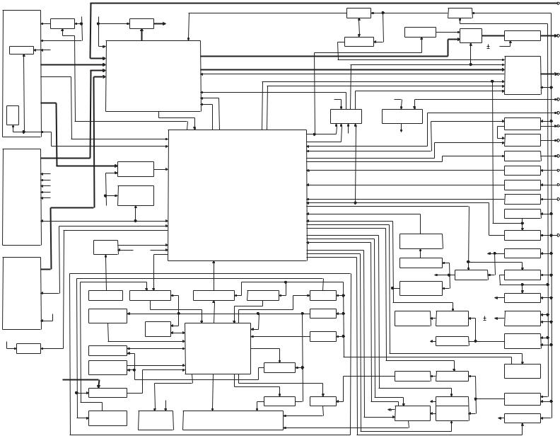
BLOCK DIAGRAM
● AC Drive + USB Mechanism unit |
|
|
|
|
|
||
DXM-6810W/DXM-6820W |
CD_Mechanism |
30Pin FFC |
|
H/U |
|
|
|
|
|
|
CN1 |
|
|
BU14V |
|
|
|
|
|
|
|
|
|
|
IC19 |
BU5.0V |
|
|
|
|
|
|
|
BU3.3V |
|
|
BU5.0V |
|
|
|
|
|
|
|
|
||
|
IC1 |
|
|
|
5V |
|
|
|
P-ON |
Mecha- |
/MSTOP |
SYS- |
P-ON |
|
|
|
|
uCOM |
|
uCOM |
|
SW-Reg. |
|
IC20,21 |
|
|
|
|
|
|
|
CS3.3V |
|
|
D5.0V |
|
|
|
|
(CS1.8V) |
|
|
|
|
|
|
|
|
|
|
|
|
|
(VBUS 5V) |
|
|
|
|
PowerON SW |
|
|
High-side |
|
|
/CS RST |
|
|
|
|
|
|
|
|
Over Current |
|
|
Switch |
|
|
|
|
|
|
|
|
|
|
IC15 |
IC25 |
|
|
|
USB_5V |
|
|
|
|
USB |
USB_D+ |
|
|
USB_D+ |
|
DECODER |
/INT |
|
|
|
USB_D- |
Cable |
|
DRIVER |
|
|
|
||||
|
/RESET |
USB_D- |
|
|
|
|
|
|
|
|
|
|
|
||
|
|
|
|
|
|
USB GND |
|
IC18 |
IC13 |
|
|
|
|
|
|
|
|
|
L-ch |
|
|
|
|
DAC |
|
LFP |
|
EVOL |
|
|
|
|
|
|
R-ch |
|
|
|
|
USB CONNECTOR
● CD player unit (X32-587)
|
|
|
|
|
|
|
|
|
|
|
|
|
|
|
|
|
|
|
|
|
|
|
|
|
|
|
|
|
|
|
|
|
|
|
|
|
|
CS POWER |
|
|
|
|
|
|
|
|
|
|
|
|
|
|
|
|
|
|
|
||||||
|
|
|
|
|
|
|
|
|
|
|
|
|
|
|
|
|
|
|
|
|
|
|
|
|
|
|
|
|
|
|
|
|
|
|
|
|
POW ON |
|
|
|
|
|
|
|
11.500MHz |
|
|
BU3.3V |
|
|
|
|
|
|
|
||||||||
|
|
|
|
|
|
|
|
|
|
|
|
|
|
|
SW3.3V(712) |
|
16.893M |
|
|
|
|
|
|
|
|
|
|
|
|
|
|
|
|
|
|
|
|
|
|
|
|
|
|
|
|
|
|
|
|
|
|
|
|
|
|
||||||||
|
|
|
|
|
|
|
|
|
|
|
|
|
|
|
|
|
|
|
|
|
|
|
|
|
|
|
|
|
|
|
|
|
|
|
|
|
|
|
|
|
|
|
|
|
|
|
|
|
|
|
|
|
|
||||||||||
|
|
|
|
|
|
|
|
|
|
|
|
|
|
|
|
|
|
|
|
|
|
|
|
|
|
|
|
|
|
|
|
|
|
|
|
|
|
|
|
|
|
|
|
|
|
|
|
|
|
|
|
|
|
|
|
|
|
|
|||||
|
|
|
|
|
|
|
|
|
|
|
|
|
|
|
|
|
|
|
|
|
|
|
|
|
|
|
|
|
|
|
|
|
|
|
|
|
|
|
|
|
|
|
|
|
|
|
|
|
|
|
|
|
|
|
|
|
Q7 |
|
|
|
|
|
|
|
|
|
|
|
|
|
|
|
|
|
|
|
|
|
|
|
|
|
|
|
|
|
|
|
|
|
|
|
|
|
|
|
|
|
|
|
|
|
|
|
|
|
|
|
|
|
|
|
|
|
|
|
|
|
|
|
3.3 |
5V |
|
|
|
|
|
|
|
|
|
|
|
|
|
|
|
|
|
|
|
|
|
|
|
|
|
|
|
|
|
|
|
|
|
|
|
|
|
|
|
|
|
A0 |
|
|
|
|
|
|
|
|
|
|
|
|
|
|
|
|
|
(SW3.3V) |
|
|
|
|
|||||
|
|
|
|
|
|
|
|
|
|
|
|
|
|
|
|
|
|
|
|
|
|
|
|
|
|
|
|
|
|
|
|
|
|
|
|
|
|
|
|
|
|
|
|
|
|
|
|
|
|
|
|
|
|
|
|
|
|
|
|
||||
|
|
DPU1 |
|
|
|
|
|
|
|
|
|
|
|
|
|
|
|
|
|
|
|
|
|
|
|
|
|
|
SI |
|
|
|
|
|
|
|
|
|
|
|
|
|
|
|
|
|
|
|
|
|
|
|
|
||||||||||
|
|
|
|
|
|
|
|
|
|
|
|
|
|
|
|
|
|
|
|
|
|
|
|
|
|
|
STB |
|
|
|
|
|
|
|
|
|
|
|
|
|
|
|
|
|
|
|
|
|
|
|
|
||||||||||||
|
|
|
|
|
|
|
|
|
|
|
|
|
|
|
|
|
|
|
|
|
|
|
|
|
|
|
|
|
|
|
|
|
|
|
|
SCK |
|
|
|
|
|
|
|
|
|
|
|
|
|
|
|
|
|
|
Q6 |
|
|
|
|
|
|||
|
|
|
|
|
LD |
|
|
|
|
|
|
|
|
|
|
|
|
|
|
|
|
|
|
|
|
|
|
|
|
|
|
|
|
|
|
|
|
|
|
|
|
|
-COM |
|
|
|
|
|
|
|
|
|
|
|
|||||||||
|
|
|
|
|
|
|
|
|
|
|
|
|
|
|
|
|
|
|
|
|
|
|
|
|
|
|
|
|
|
|
|
|
/RESET |
|
|
|
|
|
|
|
|
|
|
|
|
|
|
|
|
|
|
|
|
||||||||||
|
|
|
|
|
|
|
|
|
|
|
|
|
|
|
|
|
|
|
|
|
|
|
|
|
|
|
|
|
|
|
|
|
|
|
|
|
|
|
|
|
|
|
|
|
|
|
|
|
|
|
|
|
|
|
|
|
|
3.3 |
5V |
|
|
|
|
|
|
|
|
|
PD |
|
|
|
|
|
|
|
|
|
|
|
|
|
|
|
RF AMP |
|
|
|
|
|
|
|
SO |
|
|
|
|
|
|
|
|
|
|
IC1 |
|
|
|
|
|
|
(BU5V ) |
|
|
|
|
||||||||||||
|
|
|
|
|
|
|
|
|
|
|
|
|
|
|
|
|
|
|
|
|
|
|
|
|
|
|
|
|
|
|
|
|
|
|
|
|
|
|
|
|
|
|
|
|
|
|
|
|
|
|
|||||||||||||
|
|
|
|
|
|
|
|
|
|
|
|
|
|
|
|
|
|
|
|
|
|
SERVO DSP |
|
|
|
|
|
|
INTQ |
|
|
|
|
|
|
|
|
|
|
|
|
|
|
|
|
|
|
|
|
|
|
||||||||||||
|
|
|
|
|
E |
|
|
|
|
|
|
|
|
|
|
|
|
|
|
|
|
|
|
|
|
|
|
|
|
|
|
|
|
|
|
|
|
|
|
|
|
|
|
|
|
|
|
|
|
|
|
|
|
|
|
|
Q3 |
|
|
|
|
|
|
|
|
|
|
|
|
|
|
|
|
|
|
|
|
|
|
|
|
|
|
|
|
|
|
|
|
IC2 |
|
|
|
|
|
|
DA_EMPH |
|
|
|
|
|
|
|
|
|
|
|
|
|
|
|
|
|
|
3.3 |
5V |
|
|
|
|
||||||
|
|
|
|
|
|
|
|
|
|
|
|
|
|
|
|
|
|
|
|
|
|
|
|
|
|
|
|
|
|
|
|
|
|
|
|
|
|
|
|
|
|
|
|
|
|
|
|
||||||||||||||||
|
|
|
|
A |
B |
|
|
|
|
|
|
|
|
|
|
|
|
|
|
|
|
|
|
|
|
|
|
|
|
|
|
|
|
|
|
|
|
|
|
|
|
|
|
|
|
|
|
|
|
|
|
|
|
|
|
|
(BU5V) |
|
|
|
|
||
|
|
|
|
|
C |
|
|
|
|
|
|
|
|
|
|
|
|
|
|
|
|
|
|
|
|
|
|
|
|
|
|
|
|
|
|
|
|
|
|
/CSRST |
|
|
|
|
MUTDATA DATS |
|
|
|
|
|
|
|
|
|
|
|
|
|
|
|
|
||
|
|
|
|
|
|
|
|
|
|
|
|
|
|
|
|
|
|
|
|
|
|
|
S7.5V |
|
|
|
|
|
I2S |
|
CS3.3V & |
|
|
|
|
|
|
DATB CLK SREQ BREQ EMPHCS |
|
|
|
|
|
|
|
EMPH |
|||||||||||||||||
|
|
|
|
|
|
|
|
|
|
|
|
|
|
|
|
|
|
|
|
|
|
|
|
|
|
|
|
|
|
|
|
|
|
|
|
|
|
|
|
|
|
|
|
|
|
|
|
|
|
|
|
|
|
|
|
|
|
|
|
|
|||
|
|
|
|
|
F |
|
|
|
|
|
|
|
|
|
|
|
|
|
|
|
|
|
|
|
|
|
|
|
|
|
|
|
|
|
|
|
|
|
|
|
delay |
|
|
|
|
|
|
|
|
|
|
|
|
Infinity 0 Det. |
|||||||||
|
|
|
|
|
|
|
|
|
|
|
|
|
|
|
|
|
|
|
|
|
|
|
|
|
|
|
|
|
|
|
|
|
|
|
|
|
|
|
|
|
|
|
|
|
|
|
|
|
|
|
|
|
|
|
|
||||||||
|
|
|
|
TR COIL |
|
|
|
|
|
|
|
|
|
|
IC4 |
|
|
|
|
|
|
|
|
|
|
|
|
|
|
|
CS1.8V |
|
|
|
|
|
|
|
|
|
|
|
|
|
|
|
|
|
|
DAC_RST |
|||||||||||||
|
|
|
|
|
|
|
|
|
|
|
|
|
|
|
|
|
|
|
|
|
|
|
|
|
|
|
|
|
|
|
|
|
|
|
|
|
|
|
|
|
|
|
|
|
|
|
|
|
|
|
|
|
|
|
|
|
|
||||||
|
|
|
|
|
|
|
|
|
|
|
|
|
|
|
|
|
|
|
|
|
|
|
|
|
|
|
|
|
|
|
|
|
|
|
|
|
|
|
|
|
|
|
|
|
|
|
|
|
|
|
|
|
|
|
|
|
|
||||||
|
|
|
|
|
|
|
|
|
|
|
|
|
|
|
|
|
|
|
|
|
|
|
|
|
|
|
|
|
|
|
|
|
|
|
|
|
|
|
|
|
|
|
|
|
|
|
|
|
|
|
|
|
|
|
|
|
|
||||||
|
|
|
|
FO COIL |
|
|
|
|
|
|
|
|
|
|
|
Motor |
|
|
|
|
|
|
|
|
|
|
|
|
|
|
|
|
|
|
|
|
|
|
|
|
|
|
|
|
|
SER2(3/4Wire) |
|
|
|
|
|
|
|||||||||||
|
|
|
|
|
|
|
|
|
|
|
|
|
|
|
|
|
|
|
|
|
|
|
|
|
|
|
|
|
|
|
|
|
|
|
|
|
|
|
|
|
|
|
|
|
|
|
|
|
|
|
|
|
|
|
|
DAC_MUTE |
|||||||
|
|
|
|
|
|
|
|
|
|
|
|
|
|
|
|
|
|
Driver |
|
|
|
|
|
|
|
|
|
|
|
|
|
|
DATA |
|
|
|
|
|
|
|
|
|
|
|
|
|
|
|
|
|
|
|
|
PCM_XCK |
|||||||||
|
|
|
SP MOTOR |
|
|
|
|
|
|
|
|
|
|
|
|
|
|
|
|
|
|
|
|
|
|
|
|
|
LRCK |
|
CD I/F |
|
|
|
|
ACD DECODER |
|
PCM_DATA |
|||||||||||||||||||||||||
|
|
|
|
|
|
|
|
|
|
|
|
|
|
|
|
|
|
|
|
|
|
|
|
|
|
|
|
|
|
|
|
|
|
BCLK |
|
|
|
|
|
|
|
|
|
PCM_LRCK |
|||||||||||||||||||
|
|
Loading & sled |
|
|
|
|
|
|
|
|
|
|
|
|
|
|
|
|
|
|
|
|
|
|
|
|
|
|
|
|
|
|
|
|
|
|
|
|
MP3/WMA/AAC |
|
PCM_BCLK |
||||||||||||||||||||||
|
|
MOTOR |
|
|
|
|
|
|
|
|
|
|
|
|
|
|
|
|
|
|
|
|
|
|
|
|
C16 |
|
|
|
|
|
|
|
|
DECODER |
|
|
|
|
|
|
|
|
|
|
|
|
|||||||||||||||
|
|
|
|
|
|
|
|
|
|
|
|
|
|
|
|
|
|
|
|
|
|
|
|
|
|
|
PLL |
|
|
|
|
|
|
|
|
|
|
|
|
|
|
|
|
||||||||||||||||||||
|
|
|
|
|
CS POW |
|
|
|
|
|
|
|
|
|
|
|
|
|
|
|
|
|
|
|
|
CS3.3V |
|
|
|
|
|
|
|
|
|
|
|
|
IC15 |
|
|
|
|
|
|
|
|
|
|
|
|
||||||||||||
|
|
|
|
|
|
|
|
|
|
|
|
|
|
|
|
|
|
|
|
|
|
|
|
|
|
|
|
|
|
|
|
|
|
|
|
|
|
|
|
|
|
|
|
|
|
|
|
|
|
|
|
||||||||||||
|
|
|
|
|
|
|
|
|
|
|
|
|
|
|
|
|
|
|
|
|
IC28 |
|
(CS7410) |
|
|
|
|
|
|
|
|
|
|
|
|
|
|
|
|
|
|
|
|
|
|
|
|
|
|
|
|||||||||||||
|
|
|
|
|
POWER |
|
|
|
|
|
|
|
|
|
|
|
|
|
|
|
|
|
|
|
|
|
|
|
|
|
|
|
|
|
|
|
|
|
|
|
|
Memory |
|
|
|
|
|
|
|
|
|
|
|
|
|||||||||
|
|
|
|
|
|
|
|
|
A8V |
|
|
|
|
|
|
IC14 SW A5V |
|
|
|
|
|
|
|
|
|
|
|
|
|
|
|
|
|
|
|
|
|
|
|
|
|
|
|
|
|
|
|
|
|
|
|
|
|||||||||||
|
|
|
|
|
|
|
|
|
|
|
|
|
|
|
|
|
|
|
|
|
|
|
|
|
|
|
|
|
|
|
|
|
|
|
|
|
|
|
Controller |
|
|
|
|
|
|
|
|
|
|
|
|
||||||||||||
|
|
|
|
|
|
|
|
|
|
|
|
|
|
|
|
|
|
|
3STATE |
|
|
|
|
|
|
|
|
|
|
|
|
|
|
|
|
|
|
|
|
|
|
|
|
|
|
|
|
|
|
||||||||||||||
|
|
|
|
|
|
|
|
|
|
|
SW |
|
|
|
5V Reg. |
|
|
|
|
|
|
|
|
|
BUFFER |
|
|
|
|
|
|
|
|
|
|
|
|
|
|
|
|
|
|
|
|
|
|
|
|
|
|
|
CS3.3V |
||||||||||
|
|
|
|
|
|
|
|
|
|
|
|
|
|
|
|
|
|
|
|
|
|
|
|
|
|
|
|
|
|
|
|
|
|
|
|
|
|
|
|
|
|
|
|
|
|
|
|
|
|
||||||||||||||
D5V(D4V) |
|
|
|
|
|
|
|
|
|
|
|
|
|
|
|
|
|
|
|
|
|
|
|
|
DRAM |
|
ROM |
|
|
/CS , A20 |
|
|
(CS7410) |
||||||||||||||||||||||||||||||
|
|
|
|
|
|
|
|
|
|
|
|
|
|
|
|
|
|
|
|
|
|
|
|
|
|
|
|
|
|
|
|
|
|
|
|
|
|
|
|
|
|
|
|
|
|
||||||||||||||||||
|
|
|
|
|
|
|
|
|
|
|
|
|
|
|
|
|
|
|
|
|
|
|
|
|
|
|
|
|
|
|
|
|
4,8,16bit |
|
8bit |
|
NAND |
|
|
|
|
|
|
|
|||||||||||||||||||
|
|
|
|
|
|
|
|
|
|
|
|
|
|
|
|
|
|
|
|
|
|
|
|
|
|
|
|
|
|
|
|
|
|
|
|
|
|
|
|
|
|
|
|
|
|
|
|
|
|||||||||||||||
|
|
|
|
|
|
IC5 |
SW3.3V(712) |
|
|
|
|
|
|
|
|
|
|
|
|
|
|
CKO |
|
256K |
0 |
|
2MB |
|
GATE |
IC26 |
|
|
|
|
|
||||||||||||||||||||||||||||
|
|
|
|
|
|
|
|
|
|
|
|
|
|
|
|
|
|
|
|
|
|
|
|
|
|
|
|
|
|
|
|
|
|
|
|
|
|
|
|
/NV_CS |
|
|
|
|
|
|
|
||||||||||||||||
|
|
|
|
|
|
3.3V Reg. |
|
|
|
|
|
|
|
|
|
|
|
|
|
|
|
|
|
|
|
|
|
|
|
|
|
|
|
|
|
|
|
|
|
|
|
|
|
|
|
|
|
|
|
|
|
|
|
|
|
|
|
|
|
||||
|
|
|
|
|
|
|
|
|
|
|
CS3.3V |
|
|
|
|
|
|
|
|
|
|
|
|
|
CS3.3V |
|
|
IC16 |
|
|
|
CS3.3V |
|
|
IC17 |
CS3.3V |
|
/USB_CS |
|||||||||||||||||||||||||
|
|
|
|
|
|
|
|
|
|
|
|
|
|
|
|
|
|
|
|
|
|
|
|
|
|
|
|
|
|
||||||||||||||||||||||||||||||||||
|
|
|
|
|
|
IC21 |
(CS7410) |
|
|
|
|
|
|
|
|
|
|
|
|
|
(CS7410) |
|
|
|
|
|
(CS7410) |
|
|
(CS7410) |
|
|
|
|
|
|
|
||||||||||||||||||||||||||
|
|
|
|
|
|
|
|
|
|
|
|
|
|
|
|
|
|
|
|
|
|
|
|
|
|
|
|
|
|
|
|
|
|
|
|
|
|
|
|
|
|
|
|
|
|
|
|
|
|
Flash |
|
|
|
|
|
USB |
|
|
|
|
|
||
|
|
|
|
|
|
3.3V Reg. |
|
|
|
|
|
|
|
|
|
|
|
|
|
|
|
|
|
|
|
|
|
|
|
|
|
SDRAM |
|
|
|
|
|
|
|
|
|
|
|
|
|
|
|
|
|
|
|||||||||||||
|
|
|
|
|
|
|
|
|
|
|
|
|
|
|
|
|
|
|
|
|
|
|
|
|
|
|
|
|
|
|
|
|
|
|
|
|
|
|
|
|
|
|
|
|
|
|
|||||||||||||||||
|
|
|
|
|
|
|
|
|
|
|
|
|
|
|
|
|
|
|
|
|
|
|
|
|
|
|
|
|
|
|
|
|
|
|
|
|
|
Memory |
|
|
|
|
|
|
|
|
|
|
|||||||||||||||
|
|
|
|
|
|
|
|
|
|
|
CS1.8V |
|
|
|
|
|
|
|
|
|
|
|
|
|
|
|
|
|
|
64Mbit |
|
|
|
|
|
|
|
|
|
|
|
|
|
DRIVER |
|
|
|
|
|||||||||||||||
|
|
|
|
|
|
|
|
|
|
|
|
|
|
|
|
|
|
|
|
|
|
|
|
|
|
|
|
|
|
|
|
|
|
|
|
|
|
|
8Mbit |
|
|
|
|
|
|
|
|
||||||||||||||||
|
|
|
|
|
|
IC20 |
(CS7410) |
|
|
|
|
|
|
|
|
|
|
|
|
|
|
|
|
|
|
|
|
|
|
|
|
|
|
|
|
|
|
|
|
|
|
|
|
|
|
|
|
|
|
|
|
||||||||||||
|
|
|
|
|
|
|
|
|
|
|
|
|
|
|
|
|
|
|
|
|
|
|
|
|
|
|
|
|
|
|
|
|
|
|
|
|
|
|
|
|
|
|
|
|
|
|
|
IC25 |
|||||||||||||||
|
|
|
|
|
|
|
|
|
|
|
|
|
|
|
|
|
|
|
|
|
|
|
|
|
|
|
|
|
|
|
1M*4B*16bit |
|
|
|
|
|
|
|
|
1M*8bit |
|
|
|
|
|
|
|
|
|||||||||||||||
|
|
|
|
|
|
1.8V Reg. |
|
|
|
|
|
|
|
|
|
|
|
|
|
|
|
|
|
|
|
|
|
|
|
|
|
|
|
|
|
|
|
|
|
|
|
|
|
|
|
|
|
|
|
|
|
|
|
|
|
|
|
|
|
||||
|
|
BU5V |
|
|
|
|
|
BU3.3V |
|
|
|
|
|
|
|
|
|
|
|
|
|
|
|
|
|
|
|
|
|
|
/CSRST |
|
|
|
|
|
|
|
|
|
|
|
|
|
|
|
|
|
|
|
|||||||||||||
|
|
|
|
|
|
|
|
|
|
|
|
|
|
|
|
|
|
|
|
|
|
|
|
|
|
|
|
|
|
|
|
|
|
|
|
|
|
|
|
|
|
|
|
||||||||||||||||||||
|
|
|
|
|
|
IC19 |
|
|
|
|
|
|
|
|
|
|
|
|
|
|
|
|
|
|
|
|
|
|
|
|
|
|
|
|
|
|
|
|
|
|
|
|
|
|
|
|
|
|
|
|
|
|
|||||||||||
|
|
|
|
|
|
3.3V Reg. |
|
|
|
|
|
|
|
|
|
|
|
|
|
|
|
|
|
|
|
|
|
|
|
|
|
|
|
|
|
|
|
|
|
|
|
|
|
|
|
|
|
|
|
|
|
|
|
|
|
|
|
|
|
||||
|
|
|
|
|
|
|
|
|
|
|
|
|
|
|
|
|
|
|
|
|
|
|
|
|
|
|
|
|
|
|
|
|
|
|
|
|
|
|
|
|
|
|
|
|
|
|
|
|
|
|
|
|
|
|
|
|
|
|
|||||
|
|
|
|
|
|
|
|
|
|
|
|
|
|
|
|
|
|
|
|
|
|
|
|
|
|
|
|
|
|
|
|
|
|
|
|
|
|
|
|
|
|
|
|
|
|
|
|
|
|
|
|
|
|
|
|
|
|
|
|
|
|
|
|
CN1
LOS-SW
12EJE-SW
8EJE-SW
LOE/LIM-
I2CDATA /I2CCLK
/MRESET
/MSTOP
/AUDIO MUTE
SW A5V
CS3.3V
IC18
|
DAC |
IC13 |
SW A8V |
|
||
|
|
|
|
|
|
To |
|
|
|
LPF |
|
Audio_Lch |
MAIN |
|
|
|
|
BOARD |
||
|
|
|
|
|
Audio_Rch |
|
|
|
|
|
|
BU5 |
|
|
|
|
|
|
|
|
|
|
|
|
|
A8V |
|
|
|
|
|
|
D5V(D4V) |
|
|
|
|
|
|
S7.5 |
|
6.00MHz |
|
|
|
|
|
|
|
|
|
|
|
USB_D+ |
|
|
|
|
|
|
USB_D- |
|
|
|
|
|
|
/OC |
|
|
|
|
|
|
/PO |
|
3
DPX701/701U/701UY
DPX-MP7090U
COMPONENTS DESCRIPTION
● ELECTRIC UNIT (X34-413x-xx)
Ref. No. |
Application / Function |
Operation / Condition / Compatibility |
|
|
|
|
|
IC10 |
Audio8V Ref Power Supply |
Output 1.27V. |
|
|
|
|
|
IC80 |
Switching Regulator |
Power supply for VFD. (57V) |
|
|
|
|
|
IC100 |
Reset IC |
“L” when detection voltage goes below 3.6V or less. |
|
|
|
|
|
IC102 |
System -com |
Controls FM/AM tuner, the changer, CD/USB mechanism, Panel, volume and tone. |
|
|
|
|
|
IC103 |
Muting logic IC |
Controls logic for muting. |
|
|
|
|
|
IC104 |
EEPROM |
For instraller’s memory. |
|
|
|
|
|
IC200 |
Power Control IC |
Power control switch. |
|
|
|
|
|
IC300 |
Eelectrical Volume & Source Selecter |
Controls the source, volume, and tone. |
|
|
|
|
|
IC400 |
RDS decoder |
|
|
|
|
|
|
IC451 |
G-Analyzer |
Analog gravity sensor. |
|
|
|
|
|
IC500 |
Spectrum analyzer Buffer AMP & AGC |
It is buffer and auto gain control for spectrum analyzer. |
|
|
|
|
|
IC600 |
±9V AVR |
Power supply for 5V Pre Out OP-AMP. |
|
|
|
|
|
IC601~603 |
5V Pre-out AMP |
Output buffer and gain control. |
|
|
|
|
|
IC750 |
Power IC |
Amplifies the front L/R and the rear L/R to 50W maximum. |
|
|
|
|
|
IC800 |
Audio3.3V Ref Supply |
Audio3.3V Ref supply to electrical volume and all low pass filters. |
|
SVR6.8V Ref Supply |
SVR6.8V Ref supply to power IC. |
||
|
|||
|
|
|
|
IC901 |
Switching Regulator Controller |
Power Supply for VFD USB5V & Mecha digital. |
|
CH1: VFD & USB5V (4.7V), CH2: Mecha digital (DXM-680*: 5V ) |
|||
|
|
||
|
|
|
|
IC951 |
Power control IC |
USB power control switches with over current detection and protection. |
|
|
|
|
|
Q10,11 |
Audio8V AVR |
When Q11’s 2 pin goes Hi, A8V AVR outputs 8.0V. |
|
|
|
|
|
Q12 |
SW14V |
When Q12’s 2 pin goes Hi, SW14V outputs 14V. |
|
|
|
|
|
Q20,21 |
B.U.5V AVR |
While BU is applied, BU5V AVR outputs +5V. |
|
|
|
|
|
Q22,23 |
SW5V |
When Q23’s base goes Hi, SW5V outputs +5V. |
|
|
|
|
|
Q30,32 |
Servo+B AVR |
When Q32’s base goes Hi, Servo+B AVR outputs 8.5V. |
|
|
|
|
|
Q34 |
SW14V |
When Q12’s 2 pin goes Hi, SW14V outputs 14V. |
|
|
|
|
|
Q40,42,45 |
Panel5V AVR |
When Q42’s 2 pin goes Hi, Panel5V AVR outputs 5V. |
|
|
|
|
|
Q41,43,44 |
Illumination AVR |
When Q43’s 2 pin goes Hi, Ill AVR outputs 10.5V. |
|
|
|
|
|
Q50~52 |
SW16V (Surge Protection) |
When Q51’s 2 pin goes Hi, SW16V outputs (BU-0.6)V. |
|
|
|
|
|
Q201 |
Pre-out mute driver |
When a base gose Lo, mute driver is turned on. |
|
|
|
|
|
Q202 |
Acc Detect SW |
When Q202’s base gose Hi, Acc voltage is detected. |
|
|
|
|
|
Q204 |
Surge Detect SW |
When Q204’s base goes Hi, Surge voltage is detected. |
|
|
|
|
|
Q205 |
B.U Detected SW |
When Q35’s base gose Hi, B.U voltage is detected. |
|
|
|
|
|
Q206 |
Ext Amp Control Buffer |
It is buffer for IC102 output. |
|
|
|
|
|
Q207 |
Small-lamp Detect SW |
When Q207’s base goes Hi, Small-lamp is detected. |
|
|
|
|
|
Q208,209 |
Power Antenna SW |
When Q206’s base goes Hi, power antenna switch outputs 14V. |
|
|
|
|
|
Q210 |
Pre-out mute driver |
When a base gose Lo, mute driver is turned on. |
|
|
|
|
|
Q402,403 |
AM+B SW |
When Q403’s base gose Hi, AM+B is outputs. |
|
|
|
|
|
Q500 |
Spectrum analyzer AGC Controller |
When this circuit has an excessive input, a return is hung and an output is reduced. |
|
|
|
|
|
Q600~602 |
Pre-Amp +9V AVR |
Q600 and 602 works as a differential amplifier, Q601 works as a driver and |
|
+9.4V is supplied to OP Amp for Pre-out. |
|||
|
|
||
|
|
|
|
Q603~605 |
Pre-Amp -9V AVR |
Q603 and 605 works as a differential amplifier, Q604 works as a driver and |
|
-9.1V is supplied to OP Amp for Pre-out. |
|||
|
|
||
|
|
|
4

DPX701/701U/701UY
DPX-MP7090U
COMPONENTS DESCRIPTION
Ref. No. |
Application / Function |
|
|
Operation / Condition / Compatibility |
||
|
|
|
|
|
|
|
Q606,607 |
AUDIO 10.5V AVR |
When Q606’s base goes Hi, AVR outputs 10.5V. |
||||
|
|
|
|
|
|
|
Q608~615 |
Pre-out mute SW |
When a base gose Hi, Pre-out is set to mute. |
||||
|
|
|
|
|
|
|
Q800,802 |
REF+B AVR |
When Q800’s base goes Hi, AVR outputs 13V. |
||||
|
|
|
|
|
|
|
Q801 |
SVR6.8V Ref Supply AGC Controller |
When the voltage of B.U voltage falls, a return is hung and an output is reduced. |
||||
|
|
|
|
|
|
|
Q901 |
VFD & USB5V AVR SW |
When base goes Hi, VFD & USB5V AVR on. |
||||
|
|
|
|
|
|
|
Q902 |
Mecha digital AVR SW |
When base goes Hi, Mecha digital AVR on. (DXM-680*: 5V) |
||||
|
|
|
|
|
|
|
|
|
|
|
|
|
|
|
|
|
2pin |
L |
H |
|
|
Switching Regulator frequency |
|
1pin |
|
||
Q903 |
|
|
|
|
||
|
|
|
|
|
|
|
control SW (IC901) |
|
L |
430kHz |
600kHz |
|
|
|
|
|
||||
|
|
|
|
|
|
|
|
|
|
H |
650kHz |
820kHz |
|
|
|
|
|
|
|
|
|
|
|
|
|
|
|
Q981~983 |
SW16V (Surge Protection) |
When Q983’s 2 pin goes Hi, SW16V outputs (BU-0.6)V. |
||||
|
|
|
|
|
|
|
● SWITCH UNIT (X16-352x-xx)
Ref. No. |
Application / Function |
Operation / Condition / Compatibility |
|
|
|
IC1 |
ROM IC, Flash ROM IC |
Graphics data included. |
|
|
|
IC2 |
Spectrum analyzer IC |
6ch band pass filter. |
|
|
|
IC4 |
Panel -com |
|
|
|
|
IC6 |
Remote control IC |
Remote control receiver. |
|
|
|
IC7 |
Buffer IC |
It is change into 3.3V from 5V. |
|
|
|
IC8 |
Buffer IC |
It is change into 5V from 3.3V. |
|
|
|
IC9 |
Buffer IC |
For Control ED1. |
|
|
|
IC10 |
2.5V regulator |
The power supply For 2.5V. |
|
|
|
IC11 |
3.3V regulator |
The power supply For 3.3V. |
|
|
|
Q1 |
Triangle green LED SW |
Triangle green LED is lighting when Q1’s base level goes “H”. |
|
|
|
Q2 |
Triangle red LED SW |
Triangle red LED is lighting when Q2’s base level goes “H”. |
|
|
|
Q3 |
Key LED SW |
Key LED are lighting when Q3’s base level goes “H”. |
|
|
|
Q4,5 |
Front galss SW |
Front glass LED are lighting when Q5’s base level goes “H”. |
|
|
|
Q6 |
SW3.3V SW |
SW3.3V the power supply of IC1,3 is turned on when Q6’s base level goes “L”. |
|
|
|
Q7,8 |
SW5V SW |
SW5V the power supply of IC2,6 is turned on when Q8’s base level goes “H”. |
|
|
|
Q9,10 |
FL3.3V SW |
FL+3.3V (VDD1) is turned on when Q9’s base level goes “H”. |
|
|
|
Q11,13 |
FL+B SW |
FL+B (VDD2) is turned on when Q11’s base level goes “H”. |
|
|
|
Q12 |
FL BLK SW |
ED1 is lighted on when Q7’s base level goes “H”. |
|
|
|
Q14 |
PAN RST |
IC4 is reset when Q14's base level goes “H”. |
|
|
|
● CD PLAYER UNIT (X32-5870-00)
Ref. No. |
Application / Function |
Operation / Condition / Compatibility |
|
|
|
IC1 |
Mechanism -com |
|
|
|
|
IC2 |
Signal Processor |
|
|
|
|
IC4 |
BTL Driver |
Spindel motor, sled (including loading & eject) motor and pick-up actuator |
|
|
|
IC5 |
SW3.3V Regulator |
3.3V power supply for IC2, pick-up, IC18 digital part |
|
|
|
IC13 |
Audio Active Filter |
2nd LPF |
|
|
|
IC14 |
A5V Regulator |
3.3V power supply for DAC |
|
|
|
5
DPX701/701U/701UY
DPX-MP7090U
COMPONENTS DESCRIPTION
Ref. No. |
Application / Function |
Operation / Condition / Compatibility |
|
|
|
|
|
IC15 |
DSP for Compression Audio Decoder |
ACDrive decoder, MP3/WMA/AAC decoder |
|
|
|
|
|
IC16 |
Compression Audio Codec SDRAM |
|
|
|
|
|
|
IC17 |
Decoder Software & |
|
|
Unique ID Strage Flash ROM |
|
||
|
|
||
|
|
|
|
IC18 |
Audio D-A Converter (24-bit external) |
External 24-bit for audio |
|
|
|
|
|
IC19 |
BU3.3V Regulator |
3.3V power supply for µ-com |
|
|
|
|
|
IC20 |
1.8V Regulator |
1.8V power supply for IC15 core part |
|
|
|
|
|
IC21 |
Decoder/SDRAM/Flash ROM/ |
Power supply for decoder, SDRAM, flash ROM and USB driver. |
|
USB Driver 3.3V Regulator |
3.3V power supply for IC15 port parts, IC16, IC17, IC25, IC26 and IC28. |
||
|
|||
|
|
|
|
IC25 |
USB Host Controller |
|
|
|
|
|
|
IC26 |
Switching among IC15 & Flash ROM & |
For DSP for Compression Audio Decoder, Flash ROM, SDRAM and USB |
|
SDRAM & USB |
|||
|
|
||
|
|
|
|
IC28 |
Clock SW |
To SDRAM |
|
|
|
|
|
Q3 |
Level Shift 3.3V→5V |
|
|
|
|
|
|
Q6,7 |
Level Shift 3.3V→5V |
|
|
|
|
|
|
Q8 |
APC (Auto Power Control) |
|
|
|
|
|
|
Q9,10 |
Anticipation Sub-beam Delay |
During non-searching |
|
|
|
|
|
Q16 |
Logic Inverter |
µ-com “ZERO” terminal |
|
|
|
|
|
Q17 |
USB Hi-side SW |
|
|
|
|
|
|
Q18 |
Logic Inverter |
For DACMUTE terminal |
|
|
|
|
|
D2 |
Static Electricity Countermeasure |
For IC2 built-in reset terminal |
|
|
|
|
|
D3 |
Laser Diode Protection |
|
|
|
|
|
|
D9 |
Static Electricity Countermeasure |
|
|
|
|
|
MICROCOMPUTER’S TERMINAL DESCRIPTION
● SYSTEM MICROCOMPUTER: 30625MGPA87GP (X34: IC102)
Pin No. |
Pin Name |
Module |
I/O |
Application |
Truth |
Processing Operation Description |
|
value table |
|||||||
|
|
|
|
|
|
||
|
|
|
|
|
|
|
|
1 |
VREF |
µCOM |
- |
A/D analog reference voltage |
|
|
|
|
|
|
|
|
|
|
|
2 |
AVCC |
µCOM |
- |
|
|
|
|
|
|
|
|
|
|
|
|
3 |
LX_DATA_S |
LX_M |
I |
Data from slave unit |
|
|
|
|
|
|
|
|
|
|
|
4 |
LX_DATA_M |
LX_M |
O |
Data to slave unit |
|
|
|
|
|
|
|
|
|
|
|
5 |
LX_CLK |
LX_M |
I/O |
LX BUS clock |
|
|
|
|
|
|
|
|
|
|
|
6 |
WIRED_REMO |
EXTRA |
I |
External display remote control input |
|
|
|
|
|
|
|
|
|
|
|
6 |
NC |
|
O |
Not used when no WIRED_REMO |
|
Output L fixed |
|
|
|
|
|
|
|
|
|
7 |
LX_MUTE |
LX_M |
I |
MUTE request from slave unit |
|
H: Mute ON, L: Mute OFF |
|
|
|
|
|
|
|
|
|
8 |
AUD_SDA |
AUDIO |
O |
E-VOL data output terminal |
|
SPI communication |
|
|
|
|
|
|
|
|
|
9 |
AUD_SEL |
AUDIO |
O |
E-VOL control terminal |
|
SPI communication |
|
|
|
|
|
|
|
|
|
10 |
AUD_SCL |
AUDIO |
O |
E-VOL clock output terminal |
|
SPI communication |
|
|
|
|
|
|
|
|
6
DPX701/701U/701UY DPX-MP7090U
MICROCOMPUTER’S TERMINAL DESCRIPTION
Pin No. |
Pin Name |
Module |
I/O |
Application |
Truth |
Processing Operation Description |
|
value table |
|||||||
|
|
|
|
|
|
||
|
|
|
|
|
|
|
|
11,12 |
NC |
|
O |
Not used |
|
Output L fixed |
|
|
|
|
|
|
|
|
|
13 |
BYTE |
COM |
- |
|
|
|
|
|
|
|
|
|
|
|
|
14 |
CNVSS |
COM |
- |
|
|
|
|
|
|
|
|
|
|
|
|
15 |
XCIN |
COM |
I |
|
|
32768kHz |
|
|
|
|
|
|
|
|
|
16 |
XCOUT |
COM |
I |
|
|
32768kHz |
|
|
|
|
|
|
|
|
|
17 |
RESET |
COM |
I |
|
|
|
|
|
|
|
|
|
|
|
|
18 |
XOUT |
COM |
- |
|
|
12MHz |
|
|
|
|
|
|
|
|
|
19 |
VSS |
COM |
- |
|
|
|
|
|
|
|
|
|
|
|
|
20 |
XIN |
COM |
- |
|
|
12MHz |
|
|
|
|
|
|
|
|
|
21 |
VCC1 |
COM |
- |
|
|
|
|
|
|
|
|
|
|
|
|
22 |
NMI |
COM |
I |
Not used |
|
|
|
|
|
|
|
|
|
|
|
23 |
PANRST |
COM |
I/O |
PANRST control |
|
H: RST, Hi-Z: RST off |
|
|
|
|
|
|
|
|
|
24 |
RDS_CLK |
TUNER |
I |
RDS decoder CLK input terminal |
|
|
|
|
|
|
|
|
|
|
|
24 |
NC |
|
O |
Not used |
|
L-output for models without RDS/RBDS |
|
|
|
|
|
|
|
|
|
25 |
LX_REQ_S |
LX_M |
I |
Communication request from slave unit |
|
|
|
|
|
|
|
|
|
|
|
26 |
PON_AM |
Power supply |
I/O |
AM power supply control |
|
H: When AM, Hi-Z: When not AM |
|
|
|
|
|
|
|
|
|
27 |
LX_REQ_M |
LX_M |
O |
Communication request to the slave unit |
|
|
|
|
|
|
|
|
|
|
|
28 |
TUN_IFC_OUT |
TUNER |
I |
F/E IFC OUT input terminal |
|
H: Station found, L: Station not found |
|
|
|
|
|
|
|
|
|
29 |
NC |
|
O |
Not used |
|
Output L fixed |
|
|
|
|
|
|
|
|
|
30 |
RDS_AFS_M |
TUNER |
I/O |
Switching constant when noise detected |
r |
Refer to the truth value table |
|
|
|
|
|
|
|
|
|
30 |
NC |
|
O |
Not used in models without RDS/RBDS |
|
Output L fixed |
|
|
|
|
|
|
|
|
|
31 |
RDS_QUAL |
TUNER |
I |
RDS decoder QUAL input terminal |
|
|
|
|
|
|
|
|
|
|
|
31 |
NC |
|
O |
Not used in models without RDS/RBDS |
|
L-output for models without RDS/RBDS |
|
|
|
|
|
|
|
|
|
32 |
RDS_DATA |
TUNER |
I |
RDS decoder DATA input terminal |
|
|
|
|
|
|
|
|
|
|
|
32 |
NC |
|
O |
Not used in models without RDS/RBDS |
|
L-output for models without RDS/RBDS |
|
|
|
|
|
|
|
|
|
33 |
PWIC_BEEP |
PWIC |
O |
Beep output |
|
|
|
|
|
|
|
|
|
|
|
34 |
TUN_SCL |
TUNER |
I/O |
F/E I2C clock input/output terminal |
|
|
|
|
|
|
|
|
|
|
|
35 |
TUN_SDA |
TUNER |
I/O |
F/E I2C data input/output terminal |
|
|
|
|
|
|
|
|
|
|
|
36 |
SYS_DATA |
to PANEL |
O |
Inter-panel communication data output |
|
Data output (MAX 500kbps) |
|
terminal |
|
||||||
|
|
|
|
|
|
||
|
|
|
|
|
|
|
|
37 |
VCC1 |
COM |
- |
|
|
|
|
|
|
|
|
|
|
|
|
38 |
PAN_DATA |
to PANEL |
I |
Inter-panel communication data input |
|
Data input (MAX 500kbps) |
|
terminal |
|
||||||
|
|
|
|
|
|
||
|
|
|
|
|
|
|
|
39 |
VSS |
COM |
- |
|
|
|
|
|
|
|
|
|
|
|
|
40 |
SYS_REQ |
to PANEL |
O |
Communication request terminal from |
|
|
|
system -com |
|
|
|||||
|
|
|
|
|
|
||
|
|
|
|
|
|
|
|
41 |
PAN_REQ |
to PANEL |
I |
Communication request terminal from |
|
|
|
panel |
|
|
|||||
|
|
|
|
|
|
||
|
|
|
|
|
|
|
|
42 |
SDA/CD_SDA |
CD |
I/O |
CD mechanism I2C data input/output |
|
|
|
terminal |
|
|
|||||
|
|
|
|
|
|
||
|
|
|
|
|
|
|
|
42 |
SDA/INST_SDA |
EXTRA |
I/O |
E2PROM I2C data input/output terminal |
|
|
|
|
|
|
|
|
|
|
|
43 |
SCL/CD_SCL |
CD |
I/O |
CD mechanism I2C clock output terminal |
|
|
|
|
|
|
|
|
|
|
7
DPX701/701U/701UY DPX-MP7090U
MICROCOMPUTER’S TERMINAL DESCRIPTION
Pin No. |
Pin Name |
Module |
I/O |
Application |
Truth |
Processing Operation Description |
|
value table |
|||||||
|
|
|
|
|
|
||
|
|
|
|
|
|
|
|
43 |
SCL/INST_SCL |
EXTRA |
I/O |
E2PROM I2C clock output terminal |
|
|
|
|
|
|
|
|
|
|
|
44 |
PON_PANEL |
Power supply |
I/O |
Panel 5V control terminal |
|
H: ON, Hi-Z: Momentary power down, |
|
|
11 min. after ACC_OFF |
||||||
|
|
|
|
|
|
||
|
|
|
|
|
|
|
|
45~51 |
NC |
|
O |
Not used |
|
Output L fixed |
|
|
|
|
|
|
|
|
|
52 |
EPM |
COM |
I |
FLASH EPM input terminal |
|
|
|
|
|
|
|
|
|
|
|
53 |
NC |
|
O |
Not used |
|
Output L fixed |
|
|
|
|
|
|
|
|
|
54 |
NC (CUR DET) |
|
O |
Not used |
|
Output L fixed |
|
|
|
|
|
|
|
|
|
55 |
SW_FDC |
Power supply |
I/O |
FL tube filament power supply control |
|
ON: H |
|
terminal |
|
OFF, Display black out: Hi-Z |
|||||
|
|
|
|
|
|||
|
|
|
|
|
|
|
|
56 |
NC (SW_USB) |
|
O |
Not used |
|
Output L fixed |
|
|
|
|
|
|
|
|
|
57,58 |
NC |
|
O |
Not used |
|
Output L fixed |
|
|
|
|
|
|
|
|
|
59 |
ROMCOR_DET |
EXTRA |
I |
E2PROM writing-in request |
|
H: Writing-in |
|
|
|
|
|
|
|
|
|
60 |
NC |
|
O |
Not used |
|
Output L fixed |
|
|
|
|
|
|
|
|
|
61 |
SC_CON |
to PANEL |
O |
Inter-panel communication control |
|
POWER OFF, ACC OFF: L |
|
(CE when FLASH) |
|
||||||
|
|
|
|
|
|
||
|
|
|
|
|
|
|
|
62 |
NC |
|
O |
Not used |
|
Output L fixed |
|
|
|
|
|
|
|
|
|
63 |
TUN_TYPE1 |
TYPE |
I |
Destination setting 1 |
t |
Refer to the truth value table |
|
|
|
|
|
|
|
|
|
64 |
TUN_TYPE2 |
TYPE |
I |
Destination setting 2 |
t |
Refer to the truth value table |
|
|
|
|
|
|
|
|
|
65,66 |
NC |
|
O |
Not used |
|
Output L fixed |
|
|
|
|
|
|
|
|
|
67 |
CD_DISC12_SW |
CD |
I |
CD disc detection terminal (12cm) |
|
|
|
|
|
|
|
|
|
|
|
68 |
CD_LOS_SW |
CD |
I |
CD loading detection terminal |
|
|
|
|
|
|
|
|
|
|
|
69 |
CD_MUTE_R |
CD |
I |
CD MUTE (Rch) request terminal |
|
L: Rch mute request |
|
|
|
|
|
|
|
|
|
70 |
CD_MUTE_L |
CD |
I |
CD MUTE (Lch) request terminal |
|
L: Lch mute request |
|
|
|
|
|
|
|
|
|
71 |
CD_MRST |
CD |
O |
CD mechanism -com RST terminal |
|
H: Normal, L: RESET |
|
|
|
|
|
|
|
|
|
72 |
CD_MSTOP |
CD |
O |
CD mechanism -com stop terminal |
|
H: Mechanism -com in operation |
|
|
L: Mechanism -com stop |
||||||
|
|
|
|
|
|
||
|
|
|
|
|
|
|
|
73 |
NC |
|
O |
Not used |
|
Output L fixed |
|
|
|
|
|
|
|
|
|
74 |
CD_LOE_LIM_SW |
CD |
I |
CD detection terminal (chucking SW) |
|
H: Loading completed, L: No disc |
|
|
|
|
|
|
|
|
|
75 |
CD_LOEJ |
CD |
I/O |
CD motor control terminal |
q |
Refer to the truth value table |
|
|
|
|
|
|
|
|
|
76 |
CD_MOTOR |
CD |
O |
CD motor control terminal |
q |
Refer to the truth value table |
|
|
|
|
|
|
|
|
|
77 |
PON_ILLUMI |
Power supply |
I/O |
Key illumi power supply control |
|
H: ON, Hi-Z: OFF |
|
|
|
|
|
|
|
|
|
78 |
PON_CD |
Power supply |
I/O |
Power supply control terminal for |
|
L: When CD source |
|
CD WMA |
|
Hi-Z: When other than CD source |
|||||
|
|
|
|
|
|||
|
|
|
|
|
|
|
|
79 |
PON |
Power supply |
O |
Power supply control |
|
POWER ON: H, POWER OFF: L |
|
|
|
|
|
|
|
|
|
80 |
PON_FL+B |
Power supply |
O |
Power supply control terminal for FL |
|
POWER ON: H |
|
tube bias |
|
POWER OFF, Display black out: L |
|||||
|
|
|
|
|
|||
|
|
|
|
|
|
|
|
|
|
|
|
FL tube filament power supply |
|
POWER ON: L |
|
81 |
PON_FDC_USB |
Power supply |
I/O |
USB VBUS main power supply |
|
||
|
POWER OFF, Display black out: Hi-Z |
||||||
|
|
|
|
control terminal |
|
||
|
|
|
|
|
|
||
|
|
|
|
|
|
|
|
82 |
F_SEL1 |
EXTRA |
O |
SW-Reg frequency switching |
u |
Refer to the truth value table |
|
|
|
|
|
|
|
|
|
83 |
F_SEL2 |
EXTRA |
O |
SW-Reg frequency switching |
u |
Refer to the truth value table |
|
|
|
|
|
|
|
|
|
84 |
DIAG |
Power supply |
I/O |
PCON over-current monitoring |
|
|
|
|
|
|
|
|
|
|
8
DPX701/701U/701UY DPX-MP7090U
MICROCOMPUTER’S TERMINAL DESCRIPTION
Pin No. |
Pin Name |
Module |
I/O |
Application |
Truth |
Processing Operation Description |
|
value table |
|||||||
|
|
|
|
|
|
||
|
|
|
|
|
|
|
|
85 |
VCC2 |
COM |
- |
|
|
|
|
|
|
|
|
|
|
|
|
86 |
EXT_AMP_CON |
EXTRA |
I/O |
EXTERNAL AMP control |
|
|
|
|
|
|
|
|
|
|
|
87 |
VSS |
COM |
- |
|
|
|
|
|
|
|
|
|
|
|
|
88~91 |
TYPE_1~4 |
TYPE |
I |
Destination switching |
y |
Refer to the truth value table |
|
|
|
|
|
|
|
|
|
92 |
NC |
|
O |
Not used |
|
Output L fixed |
|
|
|
|
|
|
|
|
|
93 |
OEM_DISP_DATA |
EXTRA |
I/O |
External display DATA |
|
External display |
|
|
|
|
|
|
|
|
|
93 |
NC |
|
O |
Not used with DISP OUT |
|
Output L fixed |
|
|
|
|
|
|
|
|
|
94 |
OEM_DISP_CLK |
EXTRA |
I/O |
External display CLK |
|
External display |
|
|
|
|
|
|
|
|
|
94 |
NC |
|
O |
Not used with DISP OUT |
|
Output L fixed |
|
|
|
|
|
|
|
|
|
95 |
OEM_DISP_CE |
EXTRA |
I/O |
External display control request |
|
External display |
|
|
|
|
|
|
|
|
|
95 |
NC |
|
O |
Not used with DISP OUT |
|
Output L fixed |
|
|
|
|
|
|
|
|
|
96 |
NC |
|
O |
Not used |
|
Output L fixed |
|
|
|
|
|
|
|
|
|
97 |
P_CON |
Power supply |
O |
External amplifier control terminal |
|
POWER ON: H, POWER OFF: L, |
|
|
ALL OFF: L |
||||||
|
|
|
|
|
|
||
|
|
|
|
|
|
|
|
98 |
NC |
|
O |
Not used |
|
Output L fixed |
|
|
|
|
|
|
|
|
|
99 |
ANT_CONT |
EXTRA |
O |
Power antenna control |
|
TUNER ON: H |
|
|
|
|
|
|
|
|
|
100 |
ILLUMI_DET |
EXTRA |
I |
Dimmer illumi detection |
|
L: ON, H: OFF |
|
|
|
|
|
|
|
|
|
101 |
BU_DET |
EXTRA |
I |
Momentary power down detection |
|
L: BU found, |
|
|
H: BU not found, momentary power down |
||||||
|
|
|
|
|
|
||
|
|
|
|
|
|
|
|
102 |
ACC_DET |
EXTRA |
I |
ACC power supply detection |
|
L: ACC ON, H: ACC OFF |
|
|
|
|
|
|
|
|
|
103 |
(PWIC_SVR) |
PWIC |
O |
SVR discharging circuit |
|
H: For 5 seconds at POWER OFF |
|
|
momentary power down, L: Thereafter |
||||||
|
|
|
|
|
|
||
|
|
|
|
|
|
|
|
104 |
PWIC_MUTE |
PWIC |
O |
Power ICMUTE terminal |
|
L: While STANDBY source, momentary |
|
|
power down, L: While TEL MUTE |
||||||
|
|
|
|
|
|
||
|
|
|
|
|
|
|
|
105 |
PWIC_STBY |
PWIC |
O |
Power IC standby control |
|
POWER ON: H, POWER OFF: L |
|
|
|
|
|
|
|
|
|
106 |
LX_CON |
LX_M |
O |
Start-up request to slave unit |
|
H: Slave unit ON, L: Slave unit OFF |
|
|
|
|
|
|
|
|
|
|
|
|
|
|
|
L: When M MUTE R is L (while CD) |
|
107 |
MUTE_PRE_R |
AUDIO |
O |
PRE_OUT MUTE Rch |
|
L: At momentary power down, Fixed to |
|
|
|
|
|
|
|
H: Only when 2 zone or NAVI interruption |
|
|
|
|
|
|
|
|
|
|
|
|
|
|
|
L: When M MUTE L is L (while CD) |
|
108 |
MUTE_PRE_L |
AUDIO |
O |
PRE_OUT MUTE Lch |
|
L: At momentary power down, Fixed to |
|
|
|
|
|
|
|
H: Only when 2 zone or NAVI interruption |
|
|
|
|
|
|
|
|
|
109 |
MUTE_0 |
AUDIO |
O |
E-VOL FRONT MUTE terminal |
|
ON: L, OFF: H |
|
|
|
|
|
|
|
|
|
110 |
MUTE_1 |
AUDIO |
O |
E-VOL REAR MUTE terminal |
|
ON: L, OFF: H |
|
|
|
|
|
|
|
|
|
111 |
MUTE_2 |
AUDIO |
O |
E-VOL SW MUTE terminal |
|
ON: L, OFF: H |
|
|
|
|
|
|
|
|
|
112 |
MUTE_A |
AUDIO |
O |
E-VOL SPEANA MUTE terminal |
|
ON: L, OFF: H |
|
|
|
|
|
|
|
|
|
|
|
|
|
|
|
L: ON, H: OFF |
|
113 |
MUTE_PRE_SW |
AUDIO |
O |
PRE_OUT MUTE SUB |
|
L: At momentary power down |
|
|
Use in conjunction when using MUTE2 |
||||||
|
|
|
|
|
|
||
|
|
|
|
|
|
(antiMUTE2 shock noise measure) |
|
|
|
|
|
|
|
|
|
114 |
MUTE_AFS |
AUDIO |
O |
AFS MUTE terminal |
|
IC2’s MUTE C is used |
|
|
L: ON, H: OFF, Decay time constant 0.5ms |
||||||
|
|
|
|
|
|
||
|
|
|
|
|
|
|
9

DPX701/701U/701UY DPX-MP7090U
MICROCOMPUTER’S TERMINAL DESCRIPTION
Pin No. |
Pin Name |
Module |
I/O |
Application |
Truth |
Processing Operation Description |
|
value table |
|||||||
|
|
|
|
|
|
||
|
|
|
|
|
|
|
|
114 |
NC |
|
O |
Not used in models without RDS |
|
Output L fixed |
|
|
|
|
|
|
|
|
|
115~119 |
NC |
|
O |
Not used |
|
Output L fixed |
|
|
|
|
|
|
|
|
|
120 |
LINE_MUTE |
EXTRA |
I |
Line mute detection |
|
TEL MUTE: 1V or lower |
|
|
NAVI MUTE: 2.5V or higher |
||||||
|
|
|
|
|
|
||
|
|
|
|
|
|
|
|
121 |
NC |
|
O |
Not used |
|
Output L fixed |
|
|
|
|
|
|
|
|
|
122 |
PWIC_DC_DET |
PWIC |
I |
DC offset detection terminal |
|
|
|
|
|
|
|
|
|
|
|
123 |
LX_RST |
LX_M |
O |
Hardware-reset to slave unit |
|
H: Reset, L: Normally |
|
|
|
|
|
|
|
|
|
124 |
G_Y_OUT |
EXTRA |
I |
|
|
|
|
|
|
|
|
|
|
|
|
124 |
NC |
|
O |
Not used when without G sensor |
|
Output L fixed |
|
|
|
|
|
|
|
|
|
125 |
G_X_OUT |
EXTRA |
I |
|
|
|
|
|
|
|
|
|
|
|
|
125 |
NC |
|
O |
Not used when without G sensor |
|
Output L fixed |
|
|
|
|
|
|
|
|
|
126 |
RDS_NOISE |
TUNER |
I |
FM noise detection terminal |
|
|
|
|
|
|
|
|
|
|
|
127 |
AVSS |
COM |
- |
|
|
|
|
|
|
|
|
|
|
|
|
128 |
TUN_SMETER |
TUNER |
I |
S meter input |
|
|
|
|
|
|
|
|
|
|
Truth value table
q CD_MOTOR, CD_LOEJ
|
CD_MOTOR |
CD_LOEJ |
|
|
|
Standby |
L |
L |
|
|
|
Eject |
H |
H |
|
|
|
Load |
H |
L |
|
|
|
Brake |
H |
Hi-z |
|
|
|
r AFS processing
|
RDS_AFS_M |
RDS_AFS_L |
Status |
|
|
|
|
AFS LOW |
L |
L |
No sound output in AF search |
|
|
|
|
AFS MID |
L |
Hi-Z |
Sound output in AF search |
|
|
|
|
AFS HIGH |
Hi-Z |
Hi-Z |
Normal reception |
|
|
|
|
t TUN TYPE setting
y DESTINATION TYPE
Destination |
TYPE1 |
TYPE2 |
TYPE3 |
TYPE4 |
|
|
|
|
|
KDC-X890 |
1 |
0 |
0 |
0 |
|
|
|
|
|
KDC-MP832U |
0 |
0 |
1 |
0 |
|
|
|
|
|
KDC-X9533U |
0 |
1 |
1 |
0 |
|
|
|
|
|
DPX701U |
0 |
0 |
0 |
1 |
|
|
|
|
|
DPX701UY |
1 |
0 |
0 |
1 |
|
|
|
|
|
KDC-W7534U |
0 |
1 |
0 |
1 |
|
|
|
|
|
KDC-W7534UY |
1 |
1 |
0 |
1 |
|
|
|
|
|
U717 |
0 |
0 |
1 |
1 |
|
|
|
|
|
DPX-U099 |
1 |
0 |
1 |
1 |
|
|
|
|
|
DPX701 |
0 |
1 |
1 |
1 |
|
|
|
|
|
DPX-MP7090U |
1 |
1 |
1 |
1 |
|
|
|
|
|
|
type1 |
type2 |
u Frequency Transition |
|
|
|
|
|
|
|
|
|
|
Kenwood brand model |
L |
L |
K,M Type (10kHz space) |
|
|
|
|
|
|
|
|
|
|
Setting for OEM 1 |
L |
H |
|
Reception frequency |
FSEL1 |
FSEL2 |
|
|
|
|
|
|
|
Setting for OEM 2 |
H |
L |
|
All status excluding 530~690 AM source |
L |
L |
|
|
|
|
|
|
|
Setting for OEM 3 |
H |
H |
|
700~1020, 1390~1530 |
H |
L |
|
|
|
|
|
|
|
|
|
|
|
1540~1700 |
L |
H |
|
|
|
|
|
|
|
|
|
|
|
1030~1380 |
H |
H |
|
|
|
|
|
|
|
|
|
|
E,M Type (9kHz space) |
|
|
|
|
|
|
|
|
|
|
|
|
|
|
Reception frequency |
FSEL1 |
FSEL2 |
|
|
|
|
|
|
|
|
|
|
|
All status excluding 522~675, MW |
L |
L |
|
|
|
|
|
|
|
|
|
|
684~1017, 1386~1530 |
H |
L |
|
|
|
|
|
|
|
|
|
|
|
1539~1629 |
L |
H |
|
|
|
|
|
|
|
|
|
|
|
1026~1377 |
H |
H |
|
10
DPX701/701U/701UY DPX-MP7090U
MICROCOMPUTER’S TERMINAL DESCRIPTION
● PANEL MICROCOMPUTER: 703134AGJ011A (X16 : IC4)
Pin No. |
Pin Name |
I/O |
Application |
Processing Operation Description |
|
|
|
|
|
|
|
1~7 |
D14~D8 |
I/O |
Data input/output |
|
|
|
|
|
|
|
|
8 |
3.3VDD |
- |
3.3V |
|
|
|
|
|
|
|
|
9 |
VSS |
- |
|
|
|
|
|
|
|
|
|
10~17 |
D7~D0 |
I/O |
Data input/output |
|
|
|
|
|
|
|
|
18 |
FLGCP1 |
O |
FL tone control |
Control lighting time (brightness tone) with the pulse interval |
|
GCP=FLGCP1+FLGCP2 |
|||||
|
|
|
|
||
|
|
|
|
|
|
19 |
NC |
O |
|
Output L fixed |
|
|
|
|
|
|
|
20 |
SYS_REQ |
I |
System -com communication request input |
H: While in data communication |
|
|
|
|
|
|
|
21 |
SC_CON |
I |
System -com communication, |
H: Panel operation |
|
panel operation control |
|||||
|
|
|
|
||
|
|
|
|
|
|
22 |
FL_BK |
O |
FL BK control |
H: FL on, L: off |
|
|
|
|
|
|
|
23 |
2.5VDD |
- |
2.5V |
|
|
|
|
|
|
|
|
24 |
VSS |
- |
|
|
|
|
|
|
|
|
|
25 |
NC |
O |
Not used |
Output L fixed |
|
|
|
|
|
|
|
26,27 |
KS1, KS2 |
I/O |
Key scan output |
Output: L, Hi-z: Switching |
|
|
|
|
|
|
|
28,29 |
TD0, TD1 |
O |
Used when debugging |
NC while in normal operation |
|
|
|
|
|
|
|
30,31 |
KS3, KS4 |
I/O |
Key scan output |
Output: L, Hi-z: Switching |
|
|
|
|
|
|
|
32 |
TRST |
I |
Used when debugging |
H or L when debugging |
|
|
|
|
|
|
|
33 |
ROTARY_CCW |
I |
Rotary B input |
1 pulse/1 click |
|
24 pulse/360° |
|||||
|
|
|
|
||
|
|
|
|
|
|
34 |
ROTARY_CW |
I |
Rotary A input |
1 pulse/1 click |
|
24 pulse/360° |
|||||
|
|
|
|
||
|
|
|
|
|
|
35 |
TMS |
O |
Used when debugging |
NC while in normal operation |
|
|
|
|
|
|
|
36 |
TCM |
O |
Used when debugging |
NC while in normal operation |
|
|
|
|
|
|
|
37 |
3.3VDD |
- |
|
|
|
|
|
|
|
|
|
38 |
EVSS |
- |
|
|
|
|
|
|
|
|
|
39 |
KS5 |
I/O |
Key scan output |
Output: L, Hi-z: Switching |
|
|
|
|
|
|
|
40~42 |
KR1~KR3 |
I |
Key return input |
|
|
|
|
|
|
|
|
43 |
FLGCP2 |
O |
FL tone control |
Control lighting time (brightness tone) with the pulse interval |
|
GCP=FLGCP1+FLGCP2 |
|||||
|
|
|
|
||
|
|
|
|
|
|
44 |
PAN_REQ |
O |
Panel communication request output |
H: While in data communication |
|
|
|
|
|
|
|
45 |
SYS_DATA |
I |
Data reception from system -com |
UART communication 500kbps |
|
|
|
|
|
|
|
46 |
PAN_DATA |
O |
Data transmission from the panel |
UART communication 500kbps |
|
|
|
|
|
|
|
47 |
FL_CLK |
O |
FL serial communication reference clock |
Reference clock 4.125MHz @66MHz |
|
|
|
|
|
|
|
48 |
KR4 INT |
I |
Key return input |
Can interrupt |
|
|
|
|
|
|
|
49 |
FL_DATA1 |
O |
FL serial control data SI1 |
|
|
|
|
|
|
|
|
50 |
CLK_IN3 |
I |
Serial sync clock input |
Sync to FL_CLK |
|
|
|
|
|
|
|
51 |
FL_EN |
O |
FL skip shift control |
H or Hi-Z: Skip odd numbers, L: Skip even numbers |
|
|
|
|
|
|
|
52 |
FL_DATA2 |
O |
FL serial control data SI2 |
|
|
|
|
|
|
|
11
DPX701/701U/701UY DPX-MP7090U
MICROCOMPUTER’S TERMINAL DESCRIPTION
Pin No. |
Pin Name |
I/O |
Application |
Processing Operation Description |
|
|
|
|
|
|
|
53 |
CLK_IN2 |
I |
Serial sync clock input |
Sync to FL_CLK |
|
|
|
|
|
|
|
54 |
FL_LAT |
O |
FL latch control |
|
|
|
|
|
|
|
|
55 |
FL_DATA3 |
O |
FL serial control data SI3 |
|
|
|
|
|
|
|
|
56 |
3.3VDD |
- |
|
|
|
|
|
|
|
|
|
57,58 |
X2, X2 |
I |
Clock input |
6.6MHz, internally 66MHz |
|
|
|
|
|
|
|
59 |
CVSS |
- |
|
|
|
|
|
|
|
|
|
60 |
CKSEL |
I |
Clock generator operational mode input |
Direct connection to GND |
|
|
|
|
|
|
|
61 |
PSEL |
I |
Input frequency selection when PLL mode |
VDD connection when the main clock is 5.5MHz or above |
|
GND for other frequencies |
|||||
|
|
|
|
||
|
|
|
|
|
|
62 |
2.5VDD |
- |
|
|
|
|
|
|
|
|
|
63 |
VSS |
- |
|
|
|
|
|
|
|
|
|
64 |
MODE0 |
I |
-com operation mode input |
Direct connection to GND |
|
|
|
|
|
|
|
65 |
MODE1 |
I |
-com operation mode input |
H: Writing-in |
|
Used when debugging |
|||||
|
|
|
|
||
|
|
|
|
|
|
66 |
PAN_RST |
I |
Input from reset IC |
Cancel after 100msec after PON_PAN ON |
|
Reset after 60 sec after PON_PAN OFF |
|||||
|
|
|
|
||
|
|
|
|
|
|
67 |
AVDD1 |
I |
D/A conversion reference voltage |
Connect with D3.3V |
|
|
|
|
|
|
|
68,69 |
NC |
I |
Input-dedicated terminal |
Pull-down |
|
|
|
|
|
|
|
70,71 |
AVSS1, AVSS0 |
- |
D/A conversion reference GND |
Direct connection to GND |
|
|
|
|
|
|
|
72 |
AVDD0 |
I |
A/D conversion reference voltage |
Connect with D3.3V |
|
|
|
|
|
|
|
73 |
WAVE_IN |
I |
Audio input |
AD read |
|
|
|
|
|
|
|
74 |
F01 |
I |
BPF (63Hz) |
AD read |
|
|
|
|
|
|
|
75 |
F02 |
I |
BPF (150Hz) |
AD read |
|
|
|
|
|
|
|
76 |
F03 |
I |
BPF (330Hz) |
AD read |
|
|
|
|
|
|
|
77 |
F04 |
I |
BPF (1kHz) |
AD read |
|
|
|
|
|
|
|
78 |
F05 |
I |
BPF (3.3kHz) |
AD read |
|
|
|
|
|
|
|
79 |
F06 |
I |
BPF (10kHz) |
AD read |
|
|
|
|
|
|
|
80 |
TYPE_2 |
I |
1DIN/2DIN setting |
H: 2DIN, L: 1DIN |
|
|
|
|
|
|
|
81 |
2.5VDD |
|
|
|
|
|
|
|
|
|
|
82 |
VSS |
|
|
|
|
|
|
|
|
|
|
83 |
NC |
O |
Not used |
Output L fixed |
|
|
|
|
|
|
|
84 |
TYPE_1 |
I |
With/without customize destination setting |
H: Flash ROM, L: Mask ROM |
|
|
|
|
|
|
|
85 |
NC |
O |
|
|
|
|
|
|
|
|
|
86 |
REMO |
I |
Remote control signal input |
Detect with pulse width |
|
|
|
|
|
|
|
87 |
PON_FL+B |
O |
FL bias power switch |
H: ON, L: OFF |
|
|
|
|
|
|
|
88 |
PON_FLVDD |
I/O |
FL logic power switch |
H: ON, Hi-Z: OFF |
|
|
|
|
|
|
|
89 |
PON_5V |
I/O |
5V power switch |
Remote control IC, Spectrum analyzer IC power supply |
|
H: ON, Hi-Z: OFF |
|||||
|
|
|
|
||
|
|
|
|
|
|
90~93 |
NC |
O |
Not used |
Output L fixed |
|
|
|
|
|
|
|
94 |
WE |
I/O |
Memory data writing-in permission |
L: Writing-in, H: Wait, Hi-Z when starting up at SW3.3 |
|
|
|
|
|
|
12
DPX701/701U/701UY DPX-MP7090U
MICROCOMPUTER’S TERMINAL DESCRIPTION
Pin No. |
Pin Name |
I/O |
Application |
Processing Operation Description |
|
|
|
|
|
|
|
95 |
OE |
I/O |
Memory data transmission permission |
L: Send data, H: Wait, Hi-Z when starting up at SW3.3 |
|
|
|
|
|
|
|
96,97 |
NC |
O |
Not used |
Output L fixed |
|
|
|
|
|
|
|
98 |
3.3VDD |
|
|
|
|
|
|
|
|
|
|
99 |
VSS |
|
|
|
|
|
|
|
|
|
|
|
|
|
For product technology implementation |
Repeat H and L before finalizing |
|
100 |
FROMCHK |
O |
OK: H, NG: L (checkland needed) |
||
checking |
|||||
|
|
|
Refer to the Test Mode Specification |
||
|
|
|
|
||
|
|
|
|
|
|
100 |
NC |
O |
Not used when MASKROM |
Output L fixed |
|
|
|
|
|
|
|
101 |
CE |
I/O |
Memory operation permission |
L: Operate, H: Wait, Hi-Z when starting up at SW3.3 |
|
|
|
|
|
|
|
102~104 |
NC |
O |
Not used |
Output L fixed |
|
|
|
|
|
|
|
105 |
ROMCOR_SCL |
I/O |
For ROM correction |
Input when other than writing in (including STB) |
|
Hi-Z when starting up at SW3.3 |
|||||
|
|
|
|
||
|
|
|
|
|
|
106 |
ROMCOR_SDA |
I/O |
For ROM correction |
Input when other than writing in (including STB) |
|
Hi-Z when starting up at SW3.3 |
|||||
|
|
|
|
||
|
|
|
|
|
|
107 |
NC (SEL_E2P) |
O |
Not used |
Output L fixed |
|
|
|
|
|
|
|
108 |
PON_TRI_GREEN |
I/O |
Triangle green light on switch |
H: ON, Hi-Z: OFF, On when blackout |
|
|
|
|
|
|
|
109 |
PON_TRI_RED |
I/O |
Triangle red light on switch |
H: ON, Hi-Z: OFF |
|
|
|
|
|
|
|
110 |
PON_ILLUMI |
I/O |
Blue sub illumi, Key illumi light on switch |
H: ON, Hi-Z: OFF |
|
|
|
|
|
|
|
111 |
SA_RST |
O |
Spectrum analyzer IC reset |
H: Reset, L: Normal (spectrum analyzer IC’s RST |
|
should be 1.8V or higher) |
|||||
|
|
|
|
||
|
|
|
|
|
|
112 |
3.3VDD |
|
|
|
|
|
|
|
|
|
|
113 |
EVSS |
|
|
|
|
|
|
|
|
|
|
114 |
LIGHTING |
O |
Indirect light (blue) light on switch |
H: ON, L: OFF |
|
|
|
|
|
|
|
115 |
NC |
O |
Not used |
Output L fixed |
|
|
|
|
|
|
|
116 |
PON_SW3V |
I/O |
Kanji ROM, ROM correction |
L: ON, Hi-Z: OFF |
|
rotary encoder power supply |
|||||
|
|
|
|
||
|
|
|
|
|
|
117 |
NC |
O |
Not used |
Output L fixed |
|
|
|
|
|
|
|
118~123 |
A21~A16 |
O |
Address output |
|
|
|
|
|
|
|
|
124 |
2.5VDD |
|
|
|
|
|
|
|
|
|
|
125 |
VSS |
|
|
|
|
|
|
|
|
|
|
126~133 |
A15~A8 |
O |
Address output |
|
|
|
|
|
|
|
|
134 |
3.3VDD |
|
|
|
|
|
|
|
|
|
|
135 |
EVSS |
|
|
|
|
|
|
|
|
|
|
136~142 |
A7~A1 |
O |
Address output |
|
|
|
|
|
|
|
|
143 |
NC |
O |
Not used |
Output L fixed |
|
|
|
|
|
|
|
144 |
D15 |
I/O |
Data input/output |
|
|
|
|
|
|
|
13
DPX701/701U/701UY DPX-MP7090U
MICROCOMPUTER’S TERMINAL DESCRIPTION
● MECHANISM MICROCOMPUTER: M30620FCPGP (X32: IC1)
Pin No. |
|
|
Pin Name |
I/O |
Application |
Processing Operation Description |
||||||||
|
|
|
|
|
|
|
|
|
|
|
|
|
|
|
1~5 |
|
NC |
- |
Not used |
Opened output L fixed |
|||||||||
|
|
|
|
|
|
|
|
|
|
|
|
|
|
|
6 |
|
BYTE |
I |
External data bus SW input |
Connects to GND |
|||||||||
|
|
|
|
|
|
|
|
|
|
|
|
|
|
|
7 |
|
CNVSS |
I |
Processor mode SW |
L: Single chip mode |
|||||||||
|
H: Microprocessor mode or flash ROM writing |
|||||||||||||
|
|
|
|
|
|
|
|
|
|
|
|
|
||
|
|
|
|
|
|
|
|
|
|
|
|
|
|
|
|
|
|
|
|
|
|
|
|
|
|
|
|
|
|
8 |
|
MUTE |
O |
Audio mute control |
L: Mute ON, H: Mute OFF |
|||||||||
|
|
|
|
|
|
|
|
|
|
|
|
|
|
|
9 |
|
NC |
- |
Not used |
Opened output L fixed |
|||||||||
|
|
|
|
|
|
|
|
|
|
|
|
|
|
|
|
|
|
|
|
|
|
|
|
|
|
|
|
||
10 |
RESET |
I |
Reset detection |
L: Reset (Flash ROM writing), H: Normal |
||||||||||
|
|
|
|
|
|
|
|
|
|
|
|
|
|
|
11 |
XOUT |
O |
Main clock output |
Connects to resonator |
||||||||||
|
|
|
|
|
|
|
|
|
|
|
|
|
|
|
12 |
VSS |
- |
Power supply input |
Connects to GND |
||||||||||
|
|
|
|
|
|
|
|
|
|
|
|
|
|
|
13 |
|
XIN |
I |
Main clock input |
Connects to resonator |
|||||||||
|
|
|
|
|
|
|
|
|
|
|
|
|
|
|
14 |
|
VCC1 |
- |
Power supply input |
Connects to BU3.3V |
|||||||||
|
|
|
|
|
|
|
|
|
|
|
|
|
|
|
|
|
|
|
|
|
|
|
|
|
|
|
|||
15 |
NMI |
I |
NMI interruption input |
Input Hi (Pull-up) fixed |
||||||||||
|
|
|
|
|
|
|
|
|
|
|
|
|
|
|
|
|
|
|
|
|
|
|
|
|
|
||||
16 |
|
MSTOP |
I |
STANDBY comeback interrupption |
L: Stop, H: Stop cancelled (Hi edge) |
|||||||||
|
|
|
|
|
|
|
|
|
|
|
|
|
|
|
17 |
NC |
- |
Not used |
Opened output L fixed |
||||||||||
|
|
|
|
|
|
|
|
|
|
|
|
|
|
|
18 |
DSP INT |
I |
DSP interruption signal input |
H: Interruption (Hi edge) |
||||||||||
|
|
|
|
|
|
|
|
|
|
|
|
|
|
|
19~22 |
|
NC |
- |
Not used |
Opened output L fixed |
|||||||||
|
|
|
|
|
|
|
|
|
|
|
|
|
|
|
23 |
E2P SCL |
I/O |
E2P I2C clock output |
Series resistors and E2PROM are not built when |
||||||||||
ROM collection is not used. |
||||||||||||||
|
|
|
|
|
|
|
|
|
|
|
|
|
||
|
|
|
|
|
|
|
|
|
|
|
|
|
|
|
24 |
E2P SDA |
I/O |
E2P I2C data input and output |
Series resistors and E2PROM are not built when |
||||||||||
ROM collection is not used. |
||||||||||||||
|
|
|
|
|
|
|
|
|
|
|
|
|
||
|
|
|
|
|
|
|
|
|
|
|
|
|
|
|
25,26 |
|
NC |
- |
Not used |
Opened output L fixed |
|||||||||
|
|
|
|
|
|
|
|
|
|
|
|
|
|
|
27 |
|
SCL |
I |
System -com I2C clock input |
|
|||||||||
|
|
|
|
|
|
|
|
|
|
|
|
|
|
|
28 |
|
SDA |
I/O |
System -com I2C data input and output |
|
|||||||||
|
|
|
|
|
|
|
|
|
|
|
|
|
|
|
29 |
DSP TXD |
O |
Data output for DSP serial data |
Flash ROM writing: TXD (Pull-up) |
||||||||||
|
|
|
|
|
|
|
|
|
|
|
|
|
|
|
30 |
DSP RXD |
I |
Data input for DSP serial data |
Flash ROM writing: RXD |
||||||||||
|
|
|
|
|
|
|
|
|
|
|
|
|
|
|
31 |
DSP CLK |
O |
Clock output for DSP serial data |
Flash ROM writing: SCLK(Pull-up) |
||||||||||
|
|
|
|
|
|
|
|
|
|
|
|
|
|
|
32 |
|
DSP STB (BUSY) |
O |
DSP data strove signal output |
Flash ROM writing: BUSY |
|||||||||
|
|
|
|
|
|
|
|
|
|
|
|
|
|
|
33 |
CS SDATA |
O |
Data output for decoder serial data |
|
||||||||||
|
|
|
|
|
|
|
|
|
|
|
|
|
|
|
34 |
|
CS BDATA |
I |
Data input for decoder serial data |
|
|||||||||
|
|
|
|
|
|
|
|
|
|
|
|
|
|
|
35 |
|
CS CLK |
O |
Clock output for decoder serial data |
|
|||||||||
|
|
|
|
|
|
|
|
|
|
|
|
|
|
|
36~38 |
|
NC |
- |
Not used |
Opened output L fixed |
|||||||||
|
|
|
|
|
|
|
|
|
|
|
|
|
|
|
|
|
|
|
|
|
|
|
|
|
|||||
39 |
EPM |
- |
Not used (Flash ROM: EPM) |
Opened output L fixed |
||||||||||
|
|
|
|
|
|
|
|
|
|
|
|
|
|
|
40 |
PON D3.3 |
O |
D3.3V POWER ON control |
H: POWER ON, L: POWER OFF |
||||||||||
|
|
|
|
|
|
|
|
|
|
|
|
|
|
|
41 |
PON A5 |
O |
A5.0V POWER ON control |
H: POWER ON, L: POWER OFF |
||||||||||
|
|
|
|
|
|
|
|
|
|
|
|
|
|
|
42 |
PON CS1 |
O |
IC15 series 3.3V POWER ON control |
H: POWER ON, L: POWER OFF |
||||||||||
|
|
|
|
|
|
|
|
|
|
|
|
|
|
|
43 |
PON CS2 |
O |
IC15 series 1.8V POWER ON control |
H: POWER ON, L: POWER OFF |
||||||||||
|
|
|
|
|
|
|
|
|
|
|
|
|
|
|
44 |
|
- |
Not used (Flash ROM: CE) |
Opened output L fixed |
||||||||||
|
CE |
|
||||||||||||
|
|
|
|
|
|
|
|
|
|
|
|
|
|
|
|
|
|
|
|
|
|
|
|
||||||
45 |
DRV MUTE |
O |
Driver mute |
L: Stop, H: Mute OFF |
||||||||||
|
|
|
|
|
|
|
|
|
|
|
|
|
|
|
46,47 |
|
NC |
- |
Not used |
Opened output L fixed |
|||||||||
|
|
|
|
|
|
|
|
|
|
|
|
|
|
|
14
DPX701/701U/701UY DPX-MP7090U
MICROCOMPUTER’S TERMINAL DESCRIPTION
Pin No. |
|
Pin Name |
I/O |
Application |
Processing Operation Description |
|||
|
|
|
|
|
|
|
|
|
48 |
|
ZERO M |
I |
0-bit mute detection |
H: Mute ON, L: Mute OFF |
|||
|
(No distinction of Lch/Rch) |
|||||||
|
|
|
|
|
|
|
|
|
|
|
|
|
|
||||
49 |
DE-EMPHASIS |
O |
DAC de-emphasis control |
H: De-emphasis ON, L: De-emphasis OFF |
||||
|
|
|
|
|
|
|||
50,51 |
|
NC |
- |
Not used |
Opened output L fixed |
|||
|
|
|
|
|
|
|
|
|
52 |
|
LIM SW |
I |
Laser pick-up inner circumference detection |
H: Inner circumference |
|||
|
SW signal input |
|||||||
|
|
|
|
|
|
|
|
|
|
|
|
|
|
||||
53 |
DISC NORMAL |
O |
Media discrimination result output (Not used) |
H: Normal disc, L: Other disc |
||||
|
|
|
|
|
||||
54 |
DISC H RW |
O |
Media discrimination result output (Not used) |
H: High reflecting RW disc, L: Other disc |
||||
|
|
|
|
|
||||
55 |
DISC RW |
O |
Media discrimination result output (Not used) |
H: Normal RW disc, L: Other disc |
||||
|
|
|
|
|
|
|||
56~59 |
|
TEST OUT4~1 |
O |
Output for test |
Opened output L fixed |
|||
|
|
|
|
|
|
|||
60 |
|
VCC2 |
- |
Power supply input |
Connects to BU3.3V |
|||
|
|
|
|
|
||||
61 |
TEST OUT0 |
O |
Output for test |
Opened output L fixed |
||||
|
|
|
|
|
||||
62 |
VSS |
- |
Power supply input |
Connects to GND |
||||
|
|
|
|
|
|
|||
63~66 |
|
NC |
- |
Not used |
Opened output L fixed |
|||
|
|
|
|
|
||||
67 |
TEST IN3 |
I |
TEST IN3 |
Pull-down connection (L: Normal/H: During test) |
||||
|
|
|
|
|
||||
68 |
MODEL SEL |
I |
Model determination |
L: DXM-6810W (X32-583), H: DXM-6820W (X32-587) |
||||
|
|
|
|
|
||||
69 |
E2P WRITE |
I |
TEST IN1: E2P writing permission |
Pull-down connection (L: Normal/H: During writing) |
||||
|
|
|
|
|
||||
70 |
UNIQ ID |
I |
TEST IN0: Uniqe ID writing permission |
Pull-down connection (L: Normal/H: During writing) |
||||
|
|
|
|
|
|
|||
71~73 |
|
NC |
- |
Not used |
Opened output L fixed |
|||
|
|
|
|
|
||||
74 |
SEARCH |
O |
Searching situation output |
H: During seaching, L: Normal |
||||
|
|
|
|
|
|
|||
75,76 |
|
NC |
- |
Not used |
Opened output L fixed |
|||
|
|
|
|
|
|
|
||
|
|
|
|
|
|
|
|
|
77 |
DSP RST |
O |
DSP reset control |
L: Reset, H: Normal |
||||
|
|
|
|
|
|
|
|
|
78 |
|
DSP A0 |
O |
DSP command/parameter discrimination |
H: During parameter transmitting |
|||
|
signal output |
L: During command transmitting |
||||||
|
|
|
|
|
|
|
||
|
|
|
|
|
||||
79 |
DA EMPHASIS |
I |
DSP DA emphasis input |
H: emphasis ON, L: emphasis OFF |
||||
|
|
|
|
|
|
|||
80 |
|
ROM EMPHASIS |
I |
Decoder ROM emphasis input |
H: emphasis ON, L: emphasis OFF |
|||
|
|
|
|
|
|
|||
|
|
|
|
|
|
|
|
|
81 |
DATA MUTE |
O |
Data output status |
L: During data output muting, H: During data output |
||||
|
|
|
|
|
|
|||
82 |
|
|
|
|
|
O |
Decoder reset control |
L: Reset, H: Nornal |
|
CS RST |
|
||||||
|
|
|
|
|
||||
83 |
NC |
- |
Not used |
Opened output L fixed |
||||
|
|
|
|
|
||||
84 |
SREQ |
O |
Decoder SREQ signal output |
|
||||
|
|
|
|
|
||||
85 |
BREQ |
I |
Decoder BREQ signal input |
|
||||
|
|
|
|
|
|
|||
86~93 |
|
NC |
- |
Not used |
Opened output L fixed |
|||
|
|
|
|
|
|
|||
94 |
|
AVSS |
- |
Analog power supply input |
Connects to GND |
|||
|
|
|
|
|
||||
95 |
NC |
- |
Not used |
Opened output L fixed |
||||
|
|
|
|
|
||||
96 |
VREF |
- |
Reference voltage input |
Not used: Connects to GND |
||||
|
|
|
|
|
||||
97 |
AVCC |
- |
Analog power supply input |
Connects to BU3.3V |
||||
|
|
|
|
|
|
|||
98~100 |
|
NC |
- |
Not used |
Opened output L fixed |
|||
|
|
|
|
|
|
|
|
|
15
DPX701/701U/701UY DPX-MP7090U
TEST MODE
● How to enter the test mode
In order to enter the test mode, reset the unit while simultaneously pressing down [1] and [3] keys.
(Even when the security is set, power can be ON for 30 minutes.)
● How to clear the test mode
The test mode is cleared in case of any of the following events: resetting, momentary power down, Acc OFF and Power OFF.
● Initial conditions of the test mode
•Source is STANDBY.
•Displays lights are all turned on.
•The volume is at –10dB (The display is 30).
•Loudness (LOUD) is OFF.
•CRSC is OFF, regardless of whether there are switching functions or not.
•SYSTEM Q is NATURAL (=FLAT).
•BEEP will sound anytime with a less than 1 second push.
•Auxiliary (AUX) is ON.
•DISPLAY TYPE is TYPE D.
•Display of TUNER sources will be as follows :
European Models : Upper Display=PS/frequency, Middle Display=clock, Lower Display=Status
Other Models : Upper Display=SNPS, Middle Display =clock, Lower Display=Status
•CD/USB source display will be as follows :
Upper Display=P-TIME, Middle Display=clock, Lower Display=Status
● RDS/RBDS automatic measurement
Conventionally, the PS display has been visually checked on the production line. This will be replaced by a new processing. The PS data will be received and the PS contents is to be verified as “RDS_TEST”. When this is verified, the P-CON terminal is forced to go OFF. (In this case, “ _ ” means blank.)
→ This will be a dedicated test mode processing.
On the P-CON, when power is turned off once and, then, turned on again, (Power OFF → ON) the unit will be restarted.
● Special display when set to TUNER
When in TUNER mode, if any of the following displays appear, there is an abnormality with the front end.
•“TNE2P_NG” : Front-end E2PROM values are still default (not determined).
•“TNCON_NG” : In this condition, the communication with the front-end is not possible.
● Forced switching of K3I
In TUNER FM mode, each time [6] key is pressed, the functions move in the following cycle :
AUTO → forced WIDE → forced MIDDLE → force NARROW
→ AUTO
The initial condition is AUTO and the displays below will appear.
•AUTO : FMA
•Forced MIDDLE : FMM
•Forced WIDE : FMW
•Forced NARROW : FMN
● CD source test mode specifications
•Jumps are made to the following tracks by pressing the
[
 ] key.
No. 9 → No. 15 → No. 10 → No. 11 → No. 12 → No. 13 → No. 22 → No. 14→ No. 9 (Returns to the beginning)
It must be noted, however, that when paying MP3 / WMA / AAC disk, which contain 8 files or less, the first track and the following tracks are played in order.
•When [
 ] key is pressed, it goes down by 1 track.
•When a CD is used as a source, by pressing [1] key for less than 1 second, a jump to the Track No. 28 is made.
•When a CD is used as a source, by pressing [2] key for less than 1 second, a jump to the Track No. 14 is made.
•When a CD is used as a source, by pressing [3] key for less than 1 second, a display of CD mechanism model name and its version is made. When the pressing of [3] key for less than 1 second is made for the second time, the normal display is resumed. (Time code display)
•When a CD is used as a source, by pressing [6] key for less than 1 second, a jump to the Track No. 15 is made. At the same time, the volume value is set to 27 (5V PRE).
● Test mode specification for USB source
• While in USB source, by [6] key, set the volume value to 15.
● Audio adjust mode
•By pressing [AUD] key for less than 1 second, the Audio Adjust mode is entered.
•As with the [AUD] key, [ ] key on the remote controller can be used to enter the Audio Adjust mode.
•As for the adjustment items, items for both the AUDIO FUNCTION MODE and SETUP MODE are included.
16
DPX701/701U/701UY DPX-MP7090U
TEST MODE
•By pressing [AUD] or [FM] key briefly, switch the item to be adjusted in the following order. (only in forward rotation) The initial item will be Fader, which is followed by : Balance
→Bass Level → Middle Level → Treble Level → HPF Front
→HPF Rear → LPF Sub Woofer (After this, it will be arbitrary)
•With the remote controller, continuous forwarding is prohibited.
•Using the VOL knob and [
 ] / [
] / [
 ] key, the Fader can be adjusted in 3 steps : R15 ↔ 0 ↔ F15 (The initial value is 0)
•Using the VOL knob and [
 ] / [
] / [
 ] key, the Balance can be adjusted in 3 steps : L15 ↔ 0 ↔ R15 (The initial value is 0)
•Using the VOL knob and [
 ] / [
] / [
 ] key, the Bass / Middle / Treble Level can be adjusted in 3 steps : –8 ↔ 0 ↔ +8
(The initial value is 0)
•Using the VOL knob and [
 ] / [
] / [
 ] key, the HPF Front / Rear can be adjusted in 2 steps : Through ↔ 220Hz (The
initial value is Through)
•Using the VOL knob and [
 ] / [
] / [
 ] key, the LPF Sub Woofer can be adjusted in 2 steps : 50Hz ↔ Through (The
initial value is Through)
•Using the VOL knob and [
 ] / [
] / [
 ] key, the Sub Woofer Phase can be adjusted in 2 steps : Reverse ↔ Normal (The
initial value is Normal)
•Using the VOL knob and [
 ] / [
] / [
 ] key, the Volume Offset can be adjusted in 2 steps : –8 ↔ 0 (The initial value is
0)
•Using the VOL knob and [
 ] / [
] / [
 ] key, the Loudness ON/OFF can be adjusted in 2 steps : OFF ↔ ON (The
initial value is OFF)
•Using the VOL knob and [
 ] / [
] / [
 ] key, 2-Zone ON/OFF can be adjusted in 2 steps : OFF ↔ ON (The initial value is
OFF)
•Bass f / Bass Q / Bass EXT / Middle f / Middle Q / Treble f do no appear in audio adjustments.
● MENU items
•Press [Q] key briefly to enter the MENU.
•The [DNPP/SBF] and [DIRECT] keys on the remote controller can also be used to enter the MENU.
•With the remote controller, continuous forwarding is prohibited.
•When a CD/USB is used as a source, the default item will be the F/W Version.
● 2-ZONE (Dual Zone) items
•When using sources other than the STANDBY source, using a short-press on [AUTO] or [TI] key, 2-ZONE ON/OFF is achieved.
● Backup current measurement
When reset in Acc OFF (Back Up ON) condition, MUTE terminal goes off after 2 seconds, instead of 15 seconds. (During this time, the CD mechanism does not function.)
● OPEL communication items (OPEL communica-
tion specification supporting model)
During the test mode, OPEL communication line outputs the following (At every 500msec, the output condition of the communication line will be switched.)
CE
DATA
CLK
500msec 500msec 500msec
● G sensor display items (G-Analyzer supporting
model)
When source is STANDBY, by short-pressing [ATT] key, the display is switched to analogy meter display, in which vertical G and horizontal G are displayed.
● Special display when all lights are on
When all lights are on with the STANDBY source, the following displays are made when the keys shown below are pressed.
[1] key Version display |
|
(Display) C0528WK__SYS1. 23 |
|
(Display) |
STYPE : x__PAN1.11 |
(Display) |
PTYPE : x__MEM3.21 |
STYPE indicates system -com destination, and PTYPE indicates panel -com destination, and show real-time condition of the destination terminal (“x” is displayed in
|
hexadecimals.) |
[2] key |
Serial number display (8 digits) |
|
(Display) SNo_xxxxxxxx |
|
|
[3] key |
Key pressed briefly : Power ON time is displayed. |
|
(Display) PonTim_0Hxx_ (00~50 is displayed for “xx”. |
|
When less than 1 hour, displayed |
|
by increments of 10 minutes.) |
|
xxxxx (00001~10922 is displayed for |
|
“xxxxx”.) MAX 10922 (times) |
|
During Power On time display, by pressing for at least 2 |
|
seconds, the Power ON time is cleared. |
17
Loading...