


ICs for Communications
PLL-Frequency Synthesizer
PMB2306R/PMB2306T Version 2.2
Data Sheet 02.97
T2306-0V22-D1-7600
30% 5 30% 7 |
|
|
5HYLVLRQ +LVWRU\ |
&XUUHQW 9HUVLRQ |
|
|
|
|
Previous Version: 01.94 |
|
|
|
|
|
Page |
Page |
Subjects (major changes since last revision) |
(in previous |
(in new |
|
Version) |
Version) |
|
|
|
|
14-15 |
19-20 |
$& '& &KDUDFWHULVWLFV |
|
|
H-input current ,H: is changed from 10μA to 30μA and |
|
|
L-input current ,L: is changed from -10μA to -30μA |
|
|
|
26 |
26 |
&ORFN IUHTXHQF\ ICL max. is changed from 10MHz to 12MHz; |
|
|
+ SXOVHZLGWK &/ WWHCL min. is changed from 60ns to 40ns; |
|
|
+ SXOVHZLGWK HQDEOH WWHENmin. is changed from 60ns to 40ns; |
|
|
|
18 |
18 |
Input reference frequency ICRI is changed from 20MHz to 22MHz |
|
|
|
19 |
19 |
,QSXW 6LJQDO 5, |
|
|
Input voltage 9I: is changed from 20MHz to 22MHz |
|
|
|
(GLWLRQ
This edition was realized using the software system FrameMakerâ.
3XEOLVKHG E\ 6LHPHQV $* +/ ,7 ‹ 6LHPHQV $*
$OO 5LJKWV 5HVHUYHG $WWHQWLRQ SOHDVH
As far as patents or other rights of third parties are concerned, liability is only assumed for components, not for applications, processes and circuits implemented within components or assemblies.
The information describes the type of component and shall not be considered as assured characteristics. Terms of delivery and rights to change design reserved.
For questions on technology, delivery and prices please contact the Semiconductor Group Offices in Germany or the Siemens Companies and Representatives worldwide (see address list).
Due to technical requirements components may contain dangerous substances. For information on the types in question please contact your nearest Siemens Office, Semiconductor Group.
Siemens AG is an approved CECC manufacturer.
3DFNLQJ
Please use the recycling operators known to you. We can also help you – get in touch with your nearest sales office. By agreement we will take packing material back, if it is sorted. You must bear the costs of transport.
For packing material that is returned to us unsorted or which we are not obliged to accept, we shall have to invoice you for any costs incurred.
&RPSRQHQWV XVHG LQ OLIH VXSSRUW GHYLFHV RU V\VWHPV PXVW EH H[SUHVVO\ DXWKRUL]HG IRU VXFK SXUSRVH
Critical components1 of the Semiconductor Group of Siemens AG, may only be used in life-support devices or systems2 with the express written approval of the Semiconductor Group of Siemens AG.

30% 5 30% 7
7DEOH RI &RQWHQWV |
3DJH |
|
|
2YHUYLHZ . . . . . . . . . . . . . . . . . . . . . . . . . . . . . . . . . . . . . . . . . . . . . . . . . |
. . . .4 |
1.1 |
Features . . . . . . . . . . . . . . . . . . . . . . . . . . . . . . . . . . . . . . . . . . . . . . . . . . . |
. . .4 |
1.2 |
Pin Configuration . . . . . . . . . . . . . . . . . . . . . . . . . . . . . . . . . . . . . . . . . . . . |
. . .5 |
1.3 |
Pin Definitions and Functions . . . . . . . . . . . . . . . . . . . . . . . . . . . . . . . . . . . |
. . .6 |
1.4 |
Functional Block Diagram . . . . . . . . . . . . . . . . . . . . . . . . . . . . . . . . . . . . . |
. . .9 |
|
&LUFXLW 'HVFULSWLRQ . . . . . . . . . . . . . . . . . . . . . . . . . . . . . . . . . . . . . . . . . |
. .10 |
|
(OHFWULFDO &KDUDFWHULVWLFV . . . . . . . . . . . . . . . . . . . . . . . . . . . . . . . . . . . . |
. .18 |
3.1 |
Absolute Maximum Ratings . . . . . . . . . . . . . . . . . . . . . . . . . . . . . . . . . . . . |
. .18 |
3.2 |
Typical Supply Current ,DD . . . . . . . . . . . . . . . . . . . . . . . . . . . . . . . . . . . . . . |
. .18 |
3.3 |
AC/DC Characteristics . . . . . . . . . . . . . . . . . . . . . . . . . . . . . . . . . . . . . . . . |
. .19 |
|
3DFNDJH 2XWOLQHV . . . . . . . . . . . . . . . . . . . . . . . . . . . . . . . . . . . . . . . . . . . |
. .34 |
4.1 |
Plastic-Package, P-TSSOP-16 . . . . . . . . . . . . . . . . . . . . . . . . . . . . . . . . . |
. .34 |
4.2 |
Plastic-Package, P-DSO-14-1(SMD) . . . . . . . . . . . . . . . . . . . . . . . . . . . . . |
. .35 |
Semiconductor Group |
3 |
02.97 |
3// )UHTXHQF\ 6\QWKHVL]HU |
30% 5 30% 7 |
9HUVLRQ |
%LSRODU ,& |
|
2YHUYLHZ |
|
|
30% 7 |
|||
|
|
)HDWXUHV
• Low operating current consumption (typically 3.5 mA)
• High input sensitivity, high input frequencies (220 MHz)
• Extremely fast phase detector without dead zone
• Linearization of the phase detector output by current sources
•Synchronous programming of the counters (n-, n/a-, r-counters) and system parameters
•Fast modulus switchover for 65-MHz operation
•Switchable modulus trigger edge
•Large dividing ratios for small channel spacing
A scaler 0 to 127
N scaler 3 to 16.380 R scaler 3 to 65.535
• Serial control (3-wire bus: data, clock, enable) for fast programming (Imax ~ 10 MHz)
• Switchable polarity and phase detector current programmable
•2 Multifunction outputs
•Digital phase detector output signals (e.g. for external charge pump)
•Irn, Ivn outputs of the R and N scalers
•Port 1 output (e.g. for standby of the prescaler)
•External current setting for PD output
•Lock detect output with gated anti-backlash pulse (quasi digital lock detect)
7\SH |
9HUVLRQ |
2UGHULQJ &RGH |
3DFNDJH |
|
|
|
|
|
|
PMB 2306T |
V2.2 |
Q67100-H6423 |
P-DSO-14 |
(SMD) |
PMB 2306T |
V2.2 |
Q67106-H6423 |
P-DSO-14 |
(SMD, Tape & Reel) |
PMB 2306R |
V2.2 |
Q-67106-H6514 (T&R) |
P-TSSOP-16 (SMD, T&R) |
|
|
|
|
|
|
The PMB 2306T PLL is a high speed CMOS IC, especially designed for use in battery powered radio equipment and mobile telephones. The primary applications will be in digital systems e.g. GSM, PCN, ADC, JDC and DECT systems. The wide range of dividing ratios also allows application in modern analog systems
Semiconductor Group |
4 |
02.97 |
30% 5 30% 7
2YHUYLHZ
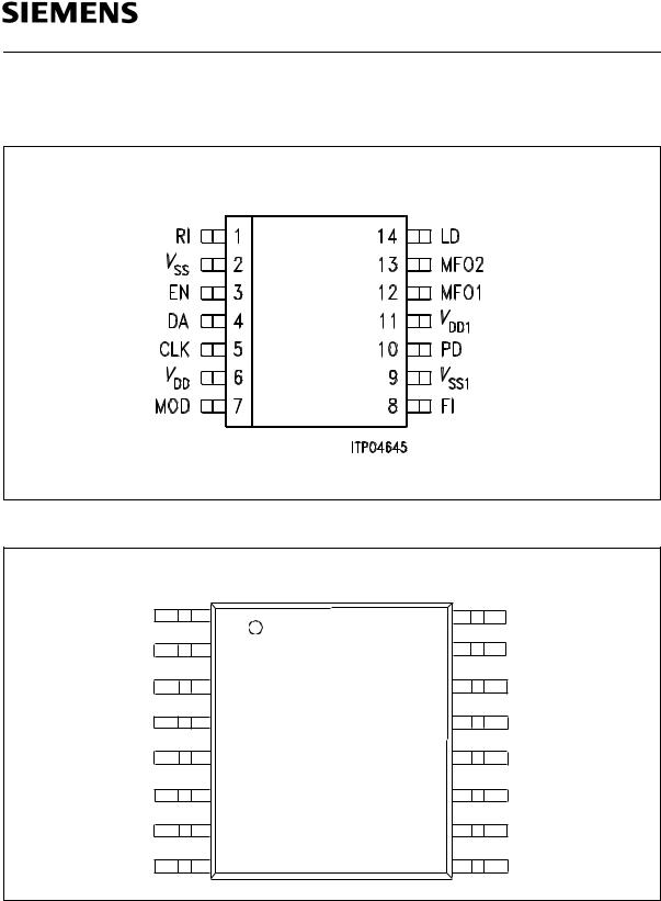
3LQ &RQILJXUDWLRQ
(top view)
3 '62
RI |
|
|
LD |
VSS |
|
|
MFO2 |
EN |
|
|
MFO1 |
DA |
|
|
VDD1 |
|
|
|
|
CLK |
|
|
PD |
VDD |
|
|
VSS1 |
MOD |
|
|
FI |
NC |
|
|
NC |
3 76623
Semiconductor Group |
5 |
02.97 |

30% 5 30% 7
2YHUYLHZ
3LQ 'HILQLWLRQV DQG )XQFWLRQV
7DEOH |
|
|
|
|
|
|
|
'62 |
76623 |
6\PERO |
)XQFWLRQ |
|
|
|
|
6 |
6 |
9DD |
Positive supply voltage for serial control logic. |
|
|
|
|
2 |
2 |
9SS |
Ground for serial control logic. |
|
|
|
|
11 |
13 |
9DD1 |
Positive supply voltage for the preamplifiers, counters, phase |
|
|
|
detector and charge pump. |
|
|
|
|
9 |
11 |
9SS1 |
Ground for the preamplifiers, counters, phase detector and |
|
|
|
charge pump. |
|
|
|
(1RWH 7KH SLQV 9'' DQG 9'' UHVSHFWLYHO\ 966 DQG 966 |
|
|
|
KDYH WR KDYH WKH VDPH VXSSO\ YROWDJH.) |
|
|
|
|
3 |
3 |
EN |
/LQH %XV (QDEOH |
|
|
|
Enable line of the serial control with internal pull-up resistor. |
|
|
|
When EN = H the input signals CLK and DA are disabled |
|
|
|
internally. When EN = L the serial control is activated. The |
|
|
|
received data are transferred into the latches with the positive |
|
|
|
edge of the EN-signal. |
|
|
|
|
4 |
4 |
DA |
/LQH %XV 'DWD |
|
|
|
Serial data input with internal pull-up resistor. The last two bits |
|
|
|
before the EN-signal define the destination address. In a byte- |
|
|
|
oriented data structure the transmitted data have to end with |
|
|
|
the EN-signal, i.e. bits to be filled in (don’t care) are transmitted |
|
|
|
first. |
|
|
|
|
5 |
5 |
CLK |
/LQH %XV &ORFN |
|
|
|
Clock line with internal pull-up resistor. The serial data are read |
|
|
|
into the internal shift register with the positive edge (see pulse |
|
|
|
diagram for serial data control). |
|
|
|
|
7 |
7 |
MOD |
0RGXOXV &RQWURO 2XWSXW for external dual modulus prescaler. |
|
|
|
The modulus output is low at the beginning of the cycle. When |
|
|
|
the a-counter has reached its set value, MOD switches to high. |
|
|
|
When the n-counter has reached its set value, MOD switches to |
|
|
|
low again, and the cycle starts from the top. When the prescaler |
|
|
|
has the counter factor P or P + 1 (P for MOD = H, P +1 for MOD |
|
|
|
= L), the overall scaling factor is NP + A. The value of the a- |
|
|
|
counter must be smaller than that of the n-counter. The trigger |
|
|
|
edge of the modulus signal to the input signal can be selected |
|
|
|
(see programming tables and MOD |
|
|
|
A, B) according to the needs of the prescaler. In single modulus |
|
|
|
operation and for standby operation in dual modulus operation, |
|
|
|
the output is low. |
|
|
|
|
Semiconductor Group |
6 |
02.97 |

30% 5 30% 7
2YHUYLHZ
7DEOH |
|
|
|
|
|
|
|
|
|
'62 |
76623 |
6\PERO |
)XQFWLRQ |
|
|
|
|
|
|
8 |
10 |
FI |
9&2 )UHTXHQF\ |
|
|
|
|
Input with highly sensitive preamplifier for 14-bit n-counter and |
|
|
|
|
7-bit a-counter. With small input signals AC coupling must be |
|
|
|
|
set up, where DC coupling can be used for large input signals. |
|
|
|
|
|
|
1 |
1 |
RI |
5HIHUHQFH )UHTXHQF\ |
|
|
|
|
Input with highly sensitive preamplifier for 16-bit r-counter. With |
|
|
|
|
small input signals AC coupling must be set up, where DC |
|
|
|
|
coupling can be used for large input signals. |
|
|
|
|
|
|
10 |
12 |
PD |
3KDVH 'HWHFWRU |
|
|
|
|
Tristate charge pump output. The integrated, positive and |
|
|
|
|
negative current sources can be programmed with respect to |
|
|
|
|
their current density by means of the serial control. Activation |
|
|
|
|
and deactivation depend on the phase relationship of the |
|
|
|
|
scaled-down input signals FI:N, RI:R. (See phase detector |
|
|
|
|
output waveforms.) |
|
|
|
|
frequency IV < IR or IV lagging: |
p-channel current source |
|
|
|
active |
|
|
|
|
frequency IV > IR or IR leading: |
n-channel current source |
|
|
|
active |
|
|
|
|
frequency IV = IR and PLL locked: current sources are |
|
|
|
|
switched off, PD-output is tristate |
|
|
|
|
In standby mode the PD-output is set to tristate. The |
|
|
|
|
assignment of the current sources to the output signals of the |
|
|
|
|
phase detector can be swapped in it’s polarity, i.e. the sign of |
|
|
|
|
the phase detector constant can be controlled. |
|
|
|
|
|
|
14 |
16 |
LD |
/RFN 'HWHFWRU 2XWSXW (open drain). Unipolar output of the |
|
|
|
|
phase detector in the form of a pulse-width modulated signal. |
|
|
|
|
The L-pulse width corresponds to the phase difference. Phase |
|
|
|
|
differences < 20 ns are not indicated due to gating of the |
|
|
|
|
antibacklash impuls. In the locked state the LD-signal is at |
|
|
|
|
H-level. In standby mode the output is resistive. |
|
|
|
|
Only for ABL status 11 no gating of ABL impulse is performed. |
|
|
|
|
|
|
Semiconductor Group |
7 |
02.97 |

30% 5 30% 7
2YHUYLHZ
7DEOH |
|
|
|
|
|
|
|
'62 |
76623 |
6\PERO |
)XQFWLRQ |
|
|
|
|
12 |
14 |
MFO1 |
0XOWLIXQFWLRQ 2XWSXW for the signals IRN, ΦV, ΦVN and port 1. |
|
|
|
|
13 |
15 |
MFO2 |
0XOWLIXQFWLRQ , 2 3LQ for the output signals IVN, ΦRN and the |
|
|
|
input signal ,REF. |
|
|
|
– The signals ΦR and ΦV are the digital output signals of the |
|
|
|
phase and frequency detector for use in external active |
|
|
|
current sources (see phase detector output wave forms). |
|
|
|
– The signals IRN and IVN are the scaled down signals of the |
|
|
|
reference frequency and VCO-frequency. The L-time |
|
|
|
corresponds to 1/IRI and 1/IFI respectively. |
|
|
|
– In the port function the port 1 output signal is assigned to the |
|
|
|
information of the status program. The output switches with |
|
|
|
the rising edge of the |
|
|
|
EN-signal. The standby mode does not affect the port |
|
|
|
function. |
|
|
|
– In the internal charge pump mode the input signal ,REF |
|
|
|
determines the value of the PD-output current. |
|
|
|
Reference current for charge pump: |
|
|
|
,REF = (9DD – 9REF)/R1 |
|
|
|
= 100μA (tolerance of ±20% or less is recommended) |
|
|
|
R1:see application circuit |
|
|
|
9REF:see AC/DC characteristics |
|
|
|
|
Semiconductor Group |
8 |
02.97 |

30% 5 30% 7
2YHUYLHZ
)XQFWLRQDO %ORFN 'LDJUDP
Semiconductor Group |
9 |
02.97 |

30% 5 30% 7
&LUFXLW 'HVFULSWLRQ
&LUFXLW 'HVFULSWLRQ
*HQHUDO 'HVFULSWLRQ
The circuit consists of a reference-, a- and n-counter, a dual modulus control logic, a phase detector with charge pump output and a serial control logic. The setting of the operating mode and the selection of the counter ratios is done serially at the ports CLK, DA and EN.
The operating modes allow the selection of single or dual operation, asynchronous or synchronous data acquisition, 4 different antibacklash-impulse times, 8 different PDoutput current modes, polarity setting of the PD-output signal, adjustment of the triggeredge of the MOD-output signal, 2 standby modes and the control of the multifunction outputs MFO1 and MFO2.
The reference frequency is applied at the RI-input and scaled down by the r-counter. It’s maximum value is 100 MHz. The VCO-frequency is applied at the FI-input and scaled down by the n- or n/a-counter according to single or dual mode operation. The maximum value at FI is 220 MHz at single-, and 65 MHz at dual mode operation.
The phase and frequency sensitive phase detector produces an output signal with adjustable anti-backlash impulses in order to prevent a dead zone for very small phase deviations. Phase differences of less than 100 ps can be resolved. In general the shortest anti-backlash pulse gives the best system performance.
3URJUDPPLQJ
Programming of the IC is done by a serial data control. The contents of the message are assigned to the functional units according to the address. 6LQJOH RU GXDO PRGH RSHUDWLRQ DV ZHOO DV DV\QFKURQRXV RU V\QFKURQRXV GDWD DFTXLVLWLRQ LV VHW E\ VWDWXV DQG VKRXOG WKHUHIRUH SUHFHGH WKH SURJUDPPLQJ RI WKH FRXQWHUV
'DWD DFTXLVLWLRQ
The PMB 2306T offers the possibility of synchronous data acquisition to avoid error signals at the phase detector due to non-corresponding dividing factors in the counters produced by asynchronous loading.
Synchronous programming guarantees control during changes of frequency or channel. That means that the state of the phase detector or the phase difference is kept maintained, and in case of “lock in”, the control process starts with the phase difference “zero”.
Semiconductor Group |
10 |
02.97 |
30% 5 30% 7
&LUFXLW 'HVFULSWLRQ
This is done as follows:
1.Setting of synchronous data acquisition by status 2.
2.Programming of the r-counter, status 1 (optional)-data is being loaded into shadow registers.
3.Programming of the n- or n/a-counter-data is being loaded into shadow registers, the EN-signal starts the synchronous loading procedure.
4.Synchronous programming – which means data transfer of all data from the shadow registers to the data registers – takes place at that point in time when the respective counter reaches “zero + 1”, the maximum repetition rate for channel change is therefore IFI:N.
5.Transfer of status 1 information into the corresponding data register is tied to the n- counter loading, but follows the loading of the n-data register in the distance of one n- counter dividing ratio, this guarantees that for example a new PD-current value becomes valid at the same time when the counters are loaded with the new data.
Synchronous avoids additional phase error caused by programming. Synchronous data acquisition is of especial advantage, when large steps in frequency are to be made in a short time. For this purpose a high reference frequency can be programmed in order to achieve rapid – “rough” – transient response. This method increases the fundamental frequency nearly by the square route of the reference frequency relation. When rough lock is achieved, another synchronous data transfer is needed to switch back to the original channel spacing. A “fine” lock in will finish the total step response. It may not be necessary to change reference frequency, but it make sense to perform synchronous data acquisition in any case. Especially for GSM, PCN, DECT, DAMPS, JDC, PHP systems the synchronous mode should be used to get best performance of the PMB 2306T.
6WDQGE\ &RQGLWLRQ
The PMB 2306T has two standby modes (standby 1, 2) to reduce the current consumption.
Standby 1 switches off the whole circuit, the current consumption is reduced below 1 μA.
Standby 2 switches off the counters, the charge pump and the outputs, only the preamplifiers stay active.
The standby modes do not affect the port output signal. For the influence on the other output signals VHH VWDQGE\ WDEOH
1RWH I51 I91 Φ51 DQG Φ91 DUH WKH LQYHUWHG VLJQDOV RI I5 I9 Φ5 DQG Φ9
Semiconductor Group |
11 |
02.97 |
 Loading...