


ICs for Consumer Electronics
Controller for Switch Mode Power Supplies Supporting Low Power Standby and Power Factor Correction
TDA 16846/TDA 16847
Data Sheet 2000-01-14
TDA 16846/TDA 16847 |
|
|
Revision History: |
Current Version: 2000-01-14 |
|
|
||
Previous Version: 1999-07-05 |
||
|
|
|
Page |
Page |
Subjects (major changes since last revision) |
(in previous |
(in current |
|
Version) |
Version) |
|
|
|
|
3 |
3, 28 |
P-DSO package added |
|
|
|
Edition 01.00
Published by Infineon Technologies AG i. Gr., St.-Martin-Strasse 53
D-81541 München
© Infineon Technologies AG 2000 All Rights Reserved.
Attention please!
The information herein is given to describe certain components and shall not be considered as warranted characteristics. Terms of delivery and rights to technical change reserved.
We hereby disclaim any and all warranties, including but not limited to warranties of non-infringement, regarding circuits, descriptions and charts stated herein.
Infineon Technologiesis an approved CECC manufacturer.
Information
For further information on technology, delivery terms and conditions and prices please contact your nearest Infineon Technologies Office in Germany or our Infineon Technologies Representatives worldwide (see address list).
Warnings
Due to technical requirements components may contain dangerous substances. For information on the types in question please contact your nearest Infineon Technologies Office.
Infineon Technologies Components may only be used in life-support devices or systems with the express written approval of Infineon Technologies, if a failure of such components can reasonably be expected to cause the failure of that life-support device or system, or to affect the safety or effectiveness of that device or system. Life support devices or systems are intended to be implanted in the human body, or to support and/or maintain and sustain and/or protect human life. If they fail, it is reasonable to assume that the health of the user or other persons may be endangered.
Controller for Switch Mode Power Supplies Supporting Low Power Standby and Power Factor Correction
Preliminary Data
TDA 16846 TDA 16847
Bipolar IC
1 |
Overview |
|
|
1.1 |
Features |
|
|
• Line Current Consumption with PFC |
P-DIP-14-3 |
||
• Low Power Consumption |
|||
|
|||
• Stable and Adjustable Standby Frequency |
|
||
• Very Low Start-up Current |
|
||
• Soft-Start for Quiet Start-up |
|
||
•Free usable Fault Comparators
•Synchronization and Fixed Frequency Facility
• Overand Undervoltage Lockout |
P-DSO-14-3 |
|
•Switch Off at Mains Undervoltage
•Temporary high power circuit (only TDA 16847)
•Mains Voltage Dependent Fold Back Point Correction
•Continuous Frequency Reduction with Decreasing Load
•Adjustable and Voltage Dependent Ringing Suppression Time
Type |
Ordering Code |
Package |
|
|
|
TDA 16846 |
Q67000-A9377 |
P-DIP-14-3 |
|
|
|
TDA 16847 |
Q67000-A9378 |
P-DIP-14-3 |
|
|
|
TDA 16846G |
Q67006-A9430 |
P-DSO-14-3 |
|
|
|
TDA 16847G |
Q67006-A9412 |
P-DSO-14-3 |
|
|
|
1.2Description
The TDA 16846 is optimized to control free running or fixed frequency flyback converters with or without Power Factor Correction (Current Pump). To provide low power consumption at light loads, this device reduces the switching frequency continuously with load, towards an adjustable minimum (e. g. 20 kHz in standby mode). Additionally, the start up current is very low. To avoid switching stresses of the power devices, the power transistor is always switched on at minimum voltage. A special circuit is implemented to avoid jitter. The device has several protection functions: VCC overand undervoltage, mains undervoltage, current limiting and 2 free usable fault comparators. Regulation can be done by using the internal error amplifier or an opto coupler feedback (additional input). The output driver is ideally suited for driving a power MOSFET, but it can also be used for a bipolar transistor. Fixed frequency and synchronized operation are also possible.
Data Sheet |
3 |
2000-01-14 |

TDA 16846
TDA 16847
The TDA 16846 is suited for TV-, VCRsets and SAT receivers. It also can be good used in PC monitors.
The TDA 16847 is identical with TDA 16846 but has an additional power measurement output (pin 8) which can be used for a Temporary High Power Circuit.
OTC |
|
1 |
|
|
|
VCC |
|
|
14 |
|
|||
PCS |
|
2 |
|
13 |
|
OUT |
|
|
|
||||
RZI |
|
3 |
|
12 |
|
GND |
|
|
|
||||
SRC |
|
4 |
|
11 |
|
PVC |
|
|
|
||||
OCI |
|
5 |
|
10 |
|
FC1 |
|
|
|
||||
FC2 |
|
6 |
|
9 |
|
REF |
|
|
|
||||
SYN |
|
7 |
|
8 |
|
N.C./PMO |
|
|
|
||||
|
|
|
|
|
|
|
AEP02647
Figure 1 Pin Configuration (top view)
1.3Pin Definitions and Functions
Pin |
Symbol |
Function |
|
|
|
|
|
1 |
OTC |
Off Time Circuit |
|
|
|
|
|
2 |
PCS |
Primary Current Simulation |
|
|
|
|
|
3 |
RZI |
Regulation and Zero Crossing Input |
|
|
|
|
|
4 |
SRC |
Soft-Start and Regulation Capacitor |
|
|
|
|
|
5 |
OCI |
Opto Coupler Input |
|
|
|
|
|
6 |
FC2 |
Fault Comparator 2 |
|
|
|
|
|
7 |
SYN |
Synchronization Input |
|
|
|
|
|
8 |
N.C./PMO |
Not Connected (TDA 16846)/PMO (TDA 16847) |
|
|
|
|
|
9 |
REF |
Reference Voltage and Current |
|
|
|
|
|
10 |
FC1 |
Fault Comparator 1 |
|
|
|
|
|
11 |
PVC |
Primary Voltage Check |
|
|
|
|
|
12 |
GND |
Ground |
|
|
|
|
|
13 |
OUT |
Output |
|
|
|
|
|
14 |
VCC |
Supply Voltage |
|
|
|
|
|
Data Sheet |
4 |
2000-01-14 |
|

TDA 16846
TDA 16847
1.4Short Description of the Pin Functions
Pin |
Function |
1 |
A parallel RC-circuit between this pin and ground determines the ringing |
|
suppression time and the standby-frequency. |
2A capacitor between this pin and ground and a resistor between this pin and the positive terminal of the primary elcap quantifies the max. possible output power of the SMPS.
3This is the input of the error amplifier and the zero crossing input. The output of a voltage divider between the control winding and ground is connected to this input. If the pulses at pin 3 exceed a 5 V threshold, the control voltage at pin 4 is lowered.
4This is the pin for the control voltage. A capacitor has to be connected between this pin and ground. The value of this capacitor determines the duration of the softstart and the speed of the control.
5If an opto coupler for the control is used, it’s output has to be connected between this pin and ground. The voltage divider at pin 3 has then to be changed, so that the pulses at pin 3 are below 5 V.
6Fault comparator 2: If a voltage > 1.2 V is applied to this pin, the SMPS stops.
7If fixed frequency mode is wanted, a parallel RC circuit has to be connected between this pin and ground. The RC-value determines the frequency. If synchronized mode is wanted, sync pulses have to be fed into this pin.
8Not connected (TDA 16846). / This is the power measurement output of the Temporary High Power Circuit. A capacitor and a RC-circuit has to be connected between this pin and ground (TDA 16847).
9 |
Output for reference voltage (5 V). With a resistor between this pin and ground |
|
the fault comparator 2 (pin 6) is enabled. |
|
|
10 |
Fault comparator 1: If a voltage > 1 V is applied to this pin, the SMPS stops. |
11This is the input of the primary voltage check. The voltage at the anode of the primary elcap has to be fed to this pin via a voltage divider. If the voltage of this pin falls below 1 V, the SMPS is switched off. A second function of this pin is the primary voltage dependent fold back point correction (only active in free running mode).
12 |
Common ground. |
13 |
Output signal. This pin has to be connected across a serial resistor with the |
|
gate of the power transistor. |
14Connection for supply voltage and startup capacitor. After startup the supply voltage is produced by the control winding of the transformer and rectified by an external diode.
Data Sheet |
5 |
2000-01-14 |
TDA 16846
TDA 16847
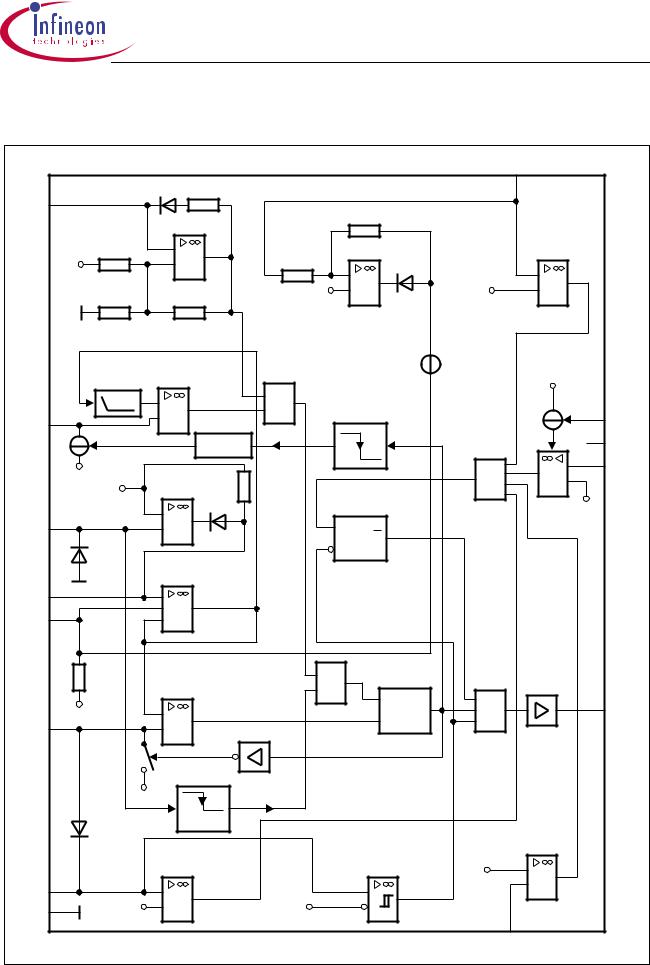
1.5Block Diagrams
|
|
|
|
|
|
|
|
|
|
|
PVC |
|
|
SYN |
7 |
|
|
D4 |
R4 |
|
Fold Back Point Correction |
|
11 |
|
|
||
|
|
|
|
|
|
R6 x 1/3 |
|
Primary |
|
||||
|
|
|
|
|
|
KSY |
|
|
|
|
|||
|
|
|
|
|
|
|
|
|
|
|
|||
|
|
|
|
R7 |
|
|
|
|
PVA |
|
Voltage |
|
|
|
5 V |
|
- |
|
R6 |
|
Check |
|
|||||
|
30 kΩ |
|
+ |
|
D5 |
|
|
|
|
||||
|
|
|
|
|
|
|
|
- |
1 V |
- |
|
|
|
|
|
|
|
|
|
|
|
+ |
+ |
|
|
||
|
|
|
|
R8 |
|
R3 |
|
|
|
|
|||
|
|
|
|
|
|
1.5 V |
|
|
|
|
|||
|
|
|
|
75 kΩ |
15 kΩ |
|
|
|
|
|
|
|
|
|
|
|
|
Control Voltage |
|
|
- |
|
|
|
|
||
|
|
|
|
|
Off Time |
|
|
3.5 V |
|
|
|
||
|
|
|
|
|
|
G1 |
|
VCC |
|
|
|||
|
|
|
|
Limit |
Comparator |
|
+ |
|
|
|
|||
|
|
|
|
|
1 |
|
|
|
|
||||
|
|
|
|
2 V |
+ |
|
|
|
|
|
|
|
|
|
1 |
|
|
|
|
ED2 |
|
|
9 |
|
|||
OTC |
CS1 |
- |
|
|
|
|
|
REF |
|||||
|
|
|
|
|
|
|
|
|
8 |
|
|||
|
|
|
|
RSTC/RSTF |
|
|
G4 |
|
N.C. |
||||
|
|
3.5 V |
5 V |
Error |
|
|
|
1 |
+ |
6 |
FC2 |
||
|
|
R2 |
|
|
|
- |
|
|
|||||
|
|
|
|
|
Amplifier |
|
Error- |
|
|
|
|
||
|
|
|
|
|
+ |
|
D2 |
|
Flipflop |
|
FC2 |
1.2 V |
|
|
3 |
|
|
|
|
|
|
|
|||||
RZI |
|
|
- |
|
|
|
S |
|
|
|
|
||
|
|
|
|
|
|
|
|
|
Q |
|
|
|
|
|
|
|
|
D3 |
Buffer for |
|
|
R |
|
|
|
|
|
|
|
|
|
|
|
|
|
|
|
|
|||
|
|
|
|
|
|
|
|
|
|
|
|
||
|
4 |
|
|
Control Voltage |
|
|
|
|
|
|
|||
SRC |
|
|
+ |
|
|
|
|
|
|
|
|
||
OCI |
5 |
|
|
+ |
|
|
|
|
|
|
|
|
|
|
|
- |
|
|
|
|
|
|
|
|
|||
|
|
|
R1 |
On Time |
|
& |
On Time |
|
Output |
|
|
||
|
|
|
|
Flipflop |
G3 |
|
|
||||||
|
|
|
20 kΩ |
Comparator |
|
|
Driver |
|
|
||||
|
|
|
|
|
S |
& |
13 |
|
|||||
|
|
|
|
|
|
|
|
|
|
|
|||
|
2 |
5 V |
|
- |
|
|
G2 |
Q |
|
OUT |
|||
PCS |
|
+ |
|
|
I1 |
R |
|
|
|
|
|||
|
|
|
|
|
|
|
|
|
|
|
|||
|
|
|
|
|
|
ED1 |
Zero Crossing |
|
|
|
|
||
|
|
|
|
1.5 V |
|
|
|
|
|
|
|||
|
|
|
|
|
|
Signal |
|
|
|
|
|||
|
|
|
|
D1 |
|
|
|
|
|
|
|
||
|
|
|
|
|
< 25 mV |
|
|
|
|
|
|
||
|
|
|
|
Startup |
|
|
|
|
|
|
|
||
|
|
|
|
|
|
|
|
Supply |
|
|
|
|
|
|
|
|
|
Diode |
Overvoltage |
|
|
|
FC1 |
|
|
||
|
|
|
|
|
|
Voltage |
|
|
|
||||
|
|
|
|
|
|
|
|
|
|
|
|||
|
14 |
|
|
Comparator |
|
|
Comparator |
1 V |
- |
|
|
||
VCC |
|
|
+ |
|
|
|
+ |
|
+ |
|
|
||
12 |
|
|
|
|
|
|
|
|
|
||||
GND |
|
16 V |
- |
|
|
15/8 V |
- |
|
10 |
|
|
||
|
|
|
|
|
|
|
|
|
|
|
|
||
|
|
|
|
|
|
|
|
|
|
|
|
|
|
|
1) |
The input with the lower voltage becomes operative |
|
|
FC1 |
AEB02648 |
|
||||||
|
|
|
|
|
|
|
|||||||
Figure 2 |
TDA 16846 |
|
Data Sheet |
6 |
2000-01-14 |

TDA 16846
TDA 16847
|
|
|
|
|
|
|
|
|
|
|
PVC |
|
|
SYN |
7 |
|
|
D4 |
R4 |
|
Fold Back Point Correction |
|
11 |
|
|
||
|
|
|
|
|
R6 x 1/3 |
|
Primary |
|
|||||
|
|
|
|
|
|
KSY |
|
|
|
||||
|
|
|
|
|
|
|
|
|
|
|
|||
|
|
|
|
R7 |
|
|
|
PVA |
|
Voltage |
|
||
|
|
|
|
|
- |
|
|
Check |
|
||||
|
5 V |
30 kΩ |
|
+ |
|
R6 |
D5 |
|
|
|
|
||
|
|
|
|
|
|
|
- |
|
1 V |
- |
|
|
|
|
|
|
|
|
|
|
+ |
|
+ |
|
|
||
|
|
|
|
R8 |
|
R3 |
|
|
|
|
|||
|
|
|
|
|
|
1.5 V |
|
|
|
|
|
||
|
|
|
|
75 kΩ |
15 kΩ |
|
|
|
|
|
|
|
|
|
|
|
|
Control Voltage |
|
|
- |
|
VCC |
|
|||
|
|
|
|
|
Off Time |
|
|
3.5 V |
|
||||
|
|
|
|
|
|
G1 |
|
|
|||||
|
|
|
|
Limit |
Comparator |
|
+ |
|
|
|
|
||
|
|
|
|
|
1 |
|
|
9 |
|
||||
|
|
|
|
2 V |
+ |
|
|
|
|
S2 |
REF |
||
OTC |
1 |
|
|
- |
|
|
ED2 |
|
|
8 |
PMO |
||
CS1 |
|
|
|
|
|
|
|
||||||
|
|
|
|
RSTC/RSTF |
|
|
G4 |
|
|
||||
|
|
|
|
|
|
|
|
|
6 |
|
|||
|
|
3.5 V |
5 V |
Error |
|
|
|
1 |
+ |
FC2 |
|||
|
|
R2 |
|
|
|
- |
|
|
|||||
|
|
|
|
|
Amplifier |
Error- |
|
|
|
|
|||
|
|
|
|
|
+ |
|
D2 |
Flipflop |
|
FC2 |
1.2 V |
|
|
|
3 |
|
|
|
|
|
|
||||||
RZI |
|
|
- |
|
|
S |
Q |
|
|
|
|
||
|
|
|
|
|
|
|
|
R |
|
|
|
|
|
|
|
|
|
D3 |
Buffer for |
|
|
|
|
|
|
||
|
|
|
|
|
|
|
|
|
|
|
|||
|
|
|
|
|
|
|
|
|
|
|
|
||
|
4 |
|
|
Control Voltage1) |
|
|
|
|
|
|
|||
SRC |
|
|
+ |
|
|
|
|
|
|
|
|
||
OCI |
5 |
|
|
+ |
|
|
|
|
|
|
|
|
|
|
|
- |
|
|
|
|
|
|
|
|
|||
|
|
|
R1 |
On Time |
|
& |
On Time |
|
Output |
|
|
||
|
|
|
|
Flipflop |
G3 |
|
|
||||||
|
|
|
20 kΩ |
Comparator |
|
|
Driver |
|
|
||||
|
|
|
|
|
S |
& |
13 |
|
|||||
|
|
|
|
|
|
|
|
|
|
|
|||
|
2 |
5 V |
|
- |
|
|
G2 |
Q |
|
OUT |
|||
PCS |
|
+ |
|
|
I1 |
R |
|
|
|
|
|||
|
|
|
|
|
|
|
|
|
|
|
|||
|
|
|
|
S1 |
|
|
|
|
Discharge Time |
|
|
|
|
|
|
|
|
|
|
ED1 |
Zero |
|
|
|
|
||
|
|
|
|
|
|
Flipflop |
|
|
|
|
|||
|
|
|
|
1.5 V |
|
|
Crossing |
S |
|
|
|
|
|
|
|
|
|
|
|
Signal |
|
|
|
|
|||
|
|
|
|
D1 |
|
|
|
Q |
|
|
|
|
|
|
|
|
|
|
< 25 mV |
|
|
|
|
|
|||
|
|
|
|
Startup |
|
|
R |
|
|
|
|
||
|
|
|
|
|
|
|
|
|
|
FC1 |
|
|
|
|
|
|
|
Diode |
Overvoltage |
|
Supply Voltage |
|
|
|
|||
|
|
|
|
|
|
1 V |
|
|
|
||||
|
|
|
|
|
Comparator |
|
Comparator |
- |
|
|
|||
VCC |
14 |
|
|
+ |
|
|
|
+ |
|
+ |
|
|
|
|
|
|
|
|
|
|
|
|
|||||
12 |
|
|
|
|
|
|
|
|
|
||||
GND |
|
16 V |
- |
|
|
15/8 V |
- |
|
10 |
|
|
||
|
|
|
|
|
|
|
|
|
|
|
|
||
|
|
|
|
|
|
|
|
|
|
|
|
|
|
|
1) |
The input with the lower voltage becomes operative |
|
|
FC1 |
AEB02737 |
|
||||||
|
|
|
|
|
|
|
|||||||
Figure 3 |
TDA 16847 |
Data Sheet |
7 |
2000-01-14 |

TDA 16846
TDA 16847
2 Functional Description
Start Up Behaviour (Pin 14)
When power is applied to the chip and the voltage V14 at Pin 14 (VCC) is less than the upper threshold (VON) of the Supply Voltage Comparator (SVC), input current I14 will be less than 100 A. The chip is not active and driver output (Pin 13) and control output (Pin 4) will be actively held low. When V14 exceeds the upper SVC threshold (VON) the chip starts working and I14 increases. When V14 falls below the lower SVC threshold (VOFF) the chip starts again at his initial condition. Figure 4 shows the start-up circuit and Figure 5 shows the voltage V14 during start up. Charging of C14 is done by resistor R2 of the “Primary Current Simulation” (see later) and the internal diode D1, so no additional start up resistor is needed. The capacitor C14 delivers the supply current until the auxiliary winding of the transformer supplies the chip with current through the external diode D14.
It is recommended to switch a small RF snubber capacitor of e.g. 100 nF parallel to the electrolytic capacitor at pin 14 as shown in the application circuits in Figures 15, 16, and 17.
|
D14 |
|
C14 |
VCC |
|
14 |
||
|
||
|
SVC |
|
|
TR |
|
C2 |
D1 |
|
PCS |
2 |
R2 |
TDA 16846 |
VOut |
Cp
AES02649
Figure 4 Startup Circuit
Data Sheet |
8 |
2000-01-14 |

TDA 16846
TDA 16847
|
Vmax |
|
V14 |
V |
|
|
On |
|
|
VOff |
|
|
Startup |
Operation |
|
|
t |
|
|
AED02650 |
Figure 5 Startup Voltage Diagram
Primary Current Simulation PCS (Pin 2) / Current Limiting
A voltage proportional to the current of the power transistor is generated at Pin 2 by the RC-combination R2, C2 (Figure 4). The voltage at Pin 2 is forced to 1.5 V when the power transistor is switched off and during its switch on time C2 is charged by R2 from the rectified mains. The relation of V2 and the current in the power transistor (Iprimary) is
:
V2 |
= 1,5 V + L---pr----imary---------×--- |
-I-pri----mary------ |
|
R2 × |
C2 |
Lprimary: Primary inductance of the transformer
The voltage V2 is applied to one input of the On Time Comparator ONTC (see Figure 2). The other input is the control voltage. If V2 exceeds the control voltage, the driver switches off (current limiting). The maximum value of the control voltage is the internal reference voltage 5 V, so the maximum current in the power transistor (IMprimary) is
:
IMprimary |
3,5 V × R2 × C2 |
= -------------------------------------- |
|
|
Lprimary |
The control voltage can be reduced by either the Error Amplifier EA (current mode regulation), or by an opto coupler at Pin 5 (regulation with opto coupler isolation) or by the voltage V11 at Pin 11 (Fold Back Point Correction).
Data Sheet |
9 |
2000-01-14 |
 Loading...