


SPP20N60C3, SPB20N60C3
SPI20N60C3, SPA20N60C3
Cool MOS™ Power Transistor |
|
VDS @ Tjmax |
650 |
V |
|
Feature |
|
|
|||
|
|
RDS(on) |
0.19 |
Ω |
|
• New revolutionary high voltage technology |
|
||||
|
ID |
20.7 |
A |
||
• Worldwide best RDS(on) in TO 220 |
|
||||
|
|
|
|
||
• Ultra low gate charge |
P-TO220-3-31 |
P-TO262-3-1 |
P-TO263-3-2 |
P-TO220-3-1 |
|
• Periodic avalanche rated |
|
|
|
|
|
• Extreme dv/dt rated |
1 |
2 3 |
|
|
|
• High peak current capability |
|
|
|
|
|
P-TO220-3-31 |
|
|
|
|
|
•Improved transconductance
•P-TO-220-3-31: Fully isolated package (2500 VAC; 1 minute)
Type |
Package |
Ordering Code |
Marking |
SPP20N60C3 |
P-TO220-3-1 |
Q67040-S4398 |
20N60C3 |
|
|
|
|
SPB20N60C3 |
P-TO263-3-2 |
Q67040-S4397 |
20N60C3 |
|
|
|
|
SPI20N60C3 |
P-TO262-3-1 |
Q67040-S4550 |
20N60C3 |
|
|
|
|
SPA20N60C3 |
P-TO220-3-31 |
Q67040-S4410 |
20N60C3 |
Maximum Ratings
Parameter |
|
Symbol |
Value |
Unit |
||
|
|
|
|
P B |
SPA |
|
|
|
|
|
SPP_B I |
|
|
Continuous drain current |
|
ID |
|
20.71) |
A |
|
T |
= 25 °C |
|
|
20.7 |
|
|
C |
|
|
|
|
|
|
T |
= 100 °C |
|
|
13.1 |
13.11) |
|
C |
|
|
|
|
|
|
Pulsed drain current, tp limited by Tjmax |
|
ID puls |
62.1 |
62.1 |
A |
|
Avalanche energy, single pulse |
|
EAS |
690 |
690 |
mJ |
|
ID=10A, VDD=50V |
|
|
|
|
|
|
Avalanche energy, repetitive t limited by T |
2) |
EAR |
1 |
1 |
|
|
|
AR |
jmax |
|
|
|
|
ID=20A, VDD=50V |
|
|
|
|
|
|
Avalanche current, repetitive tAR limited by Tjmax |
IAR |
20 |
20 |
A |
||
Gate source voltage static |
|
VGS |
±20 |
±20 |
V |
|
Gate source voltage AC (f >1Hz) |
|
VGS |
±30 |
±30 |
|
|
Power dissipation, TC = 25°C |
|
Ptot |
208 |
34.5 |
W |
|
Operating and storage temperature |
|
Tj , Tstg |
-55...+150 |
°C |
||
Rev.2.1 |
Page 1 |
2004-09-07 |

SPP20N60C3, SPB20N60C3
SPI20N60C3, SPA20N60C3
Maximum Ratings
|
Parameter |
|
|
|
|
Symbol |
|
|
|
Value |
|
|
Unit |
|
|
Drain Source voltage slope |
|
|
|
|
dv/dt |
|
|
50 |
|
|
V/ns |
||
|
VDS = 480 V, ID = 20.7 A, Tj = 125 °C |
|
|
|
|
|
|
|
|
|
|
|
|
|
|
Thermal Characteristics |
|
|
|
|
|
|
|
|
|
|
|
|
|
|
Parameter |
|
|
|
|
Symbol |
|
|
|
Values |
|
|
Unit |
|
|
|
|
|
|
|
|
|
min. |
|
typ. |
|
max. |
|
|
|
Thermal resistance, junction - case |
|
|
RthJC |
- |
- |
0.6 |
K/W |
||||||
|
Thermal resistance, junction - case, FullPAK |
|
|
RthJC_FP |
- |
- |
3.6 |
|
|
|||||
|
Thermal resistance, junction - ambient, leaded |
|
RthJA |
- |
- |
62 |
|
|
||||||
|
Thermal resistance, junction - ambient, FullPAK |
|
RthJA_FP |
- |
- |
80 |
|
|
||||||
|
SMD version, device on PCB: |
|
|
|
|
RthJA |
|
|
|
|
|
|
|
|
|
@ min. footprint |
|
|
|
|
|
- |
- |
62 |
|
|
|||
|
@ 6 cm2 cooling area 3) |
|
|
|
|
|
- |
35 |
- |
|
|
|||
|
Soldering temperature, |
|
|
|
|
Tsold |
- |
- |
260 |
°C |
||||
|
1.6 mm (0.063 in.) from case for 10s 4) |
|
|
|
|
|
|
|
|
|
|
|
||
|
Electrical Characteristics, at Tj=25°C unless otherwise specified |
|
|
|
|
|
|
|||||||
|
Parameter |
Symbol |
|
Conditions |
|
|
|
Values |
|
|
Unit |
|||
|
|
|
|
|
|
|
|
min. |
|
typ. |
|
max. |
|
|
|
Drain-source breakdown voltage |
V(BR)DSS |
VGS=0V, ID=0.25mA |
|
600 |
|
- |
|
- |
V |
||||
|
Drain-Source avalanche |
V(BR)DS |
|
VGS=0V, ID=20A |
|
- |
|
700 |
|
- |
|
|
||
|
breakdown voltage |
|
|
|
|
|
|
|
|
|
|
|
|
|
|
|
|
|
|
|
|
|
|
|
|
|
|
||
|
Gate threshold voltage |
VGS(th) |
|
ID=1000 A, VGS=VD |
|
2.1 |
|
3 |
|
3.9 |
|
|
||
|
Zero gate voltage drain current |
IDSS |
|
VDS=600V, VGS=0V, |
|
|
|
|
|
|
µA |
|||
|
|
|
|
Tj=25°C |
|
|
- |
|
0.1 |
|
1 |
|
|
|
|
|
|
|
Tj=150°C |
|
|
- |
|
- |
|
100 |
|
|
|
|
Gate-source leakage current |
IGSS |
|
VGS=30V, VDS=0V |
|
- |
|
- |
|
100 |
nA |
|||
|
Drain-source on-state resistance |
RDS(on) |
|
VGS=10V, ID=13.1A |
|
|
|
|
|
|
Ω |
|||
|
|
|
|
Tj=25°C |
|
|
- |
|
0.16 |
|
0.19 |
|
|
|
|
|
|
|
Tj=150°C |
|
|
- |
|
0.43 |
|
- |
|
|
|
|
Gate input resistance |
RG |
|
f=1MHz, open drain |
|
- |
|
0.54 |
|
- |
|
|
||
Rev.2.1 |
Page 2 |
2004-09-07 |

SPP20N60C3, SPB20N60C3
SPI20N60C3, SPA20N60C3
Electrical Characteristics
Parameter |
Symbol |
Conditions |
|
Values |
|
Unit |
|
|
|
min. |
typ. |
max. |
|
Transconductance |
gfs |
VDS≥ 2*ID*RDS(on)max, |
- |
17.5 |
- |
S |
|
|
ID=13.1A |
|
|
|
|
Input capacitance |
Ciss |
VGS=0V, VDS=25V, |
- |
2400 |
- |
pF |
Output capacitance |
Coss |
f=1MHz |
- |
780 |
- |
|
Reverse transfer capacitance |
Crss |
|
- |
50 |
- |
|
Effective output capacitance,5) |
Co(er) |
VGS=0V, |
- |
83 |
- |
|
energy related |
|
VDS=0V to 480V |
|
|
|
|
Effective output capacitance,6) |
Co(tr) |
|
- |
160 |
- |
|
time related |
|
|
|
|
|
|
|
|
|
|
|
|
|
Turn-on delay time |
td(on) |
VDD=380V, VGS=0/13V, |
- |
10 |
- |
ns |
|
|
ID=20.7A, |
|
|
|
|
|
|
RG=3.6Ω , Tj=125 |
|
|
|
|
Rise time |
tr |
VDD=380V, VGS=0/13V, |
- |
5 |
- |
|
Turn-off delay time |
td(off) |
ID=20.7A, |
- |
67 |
100 |
|
Fall time |
t |
RG=3.6Ω |
- |
4.5 |
12 |
|
|
f |
|
|
|
|
|
Gate Charge Characteristics |
|
|
|
|
|
|
Gate to source charge |
Qgs |
VDD=480V, ID=20.7A |
- |
11 |
- |
nC |
Gate to drain charge |
Qgd |
|
- |
33 |
- |
|
Gate charge total |
Qg |
VDD=480V, ID=20.7A, |
- |
87 |
114 |
|
|
|
VGS=0 to 10V |
|
|
|
|
Gate plateau voltage |
V(plateau) |
VDD=480V, ID=20.7A |
- |
5.5 |
- |
V |
1Limited only by maximum temperature
2Repetitve avalanche causes additional power losses that can be calculated asPAV=EAR*f.
3Device on 40mm*40mm*1.5mm epoxy PCB FR4 with 6cm² (one layer, 70 µm thick) copper area for drain connection. PCB is vertical without blown air.
4Soldering temperature for TO-263: 220°C, reflow
5Co(er) is a fixed capacitance that gives the same stored energy as Coss while VDS is rising from 0 to 80% VDSS. 6Co(tr) is a fixed capacitance that gives the same charging time as Coss while VDS is rising from 0 to 80% VDSS.
Rev.2.1 |
Page 3 |
2004-09-07 |
SPP20N60C3, SPB20N60C3
SPI20N60C3, SPA20N60C3
Electrical Characteristics
Parameter |
|
|
|
|
|
|
|
|
|
|
|
|
|
|
|
|
|
|
|
|
|
|
|
|
|
|
|
|
|
|
|
|
|
|
|
Symbol |
|
|
|
|
|
|
|
|
|
|
|
Conditions |
|
|
|
|
|
|
|
|
Values |
|
|
Unit |
||||||||||||||||||||||||||||||||||||||
|
|
|
|
|
|
|
|
|
|
|
|
|
|
|
|
|
|
|
|
|
|
|
|
|
|
|
|
|
|
|
|
|
|
|
|
|
|
|
|
|
|
|
|
|
|
|
|
|
|
|
|
|
|
|
|
|
|
|
|
|
|
|
|
|
|
|
|
|
|
|
|
|
|
|
|
|
|
|
|
|
min. |
|
|
typ. |
|
max. |
|
|||||||||||
Inverse diode continuous |
|
|
|
|
|
|
|
|
|
|
|
|
|
|
IS |
|
|
|
|
|
|
|
|
|
|
|
TC=25°C |
|
|
|
- |
|
|
|
- |
|
|
|
|
20.7 |
A |
|||||||||||||||||||||||||||||||||||||||||||||||||||||||||
forward current |
|
|
|
|
|
|
|
|
|
|
|
|
|
|
|
|
|
|
|
|
|
|
|
|
|
|
|
|
|
|
|
|
|
|
|
|
|
|
|
|
|
|
|
|
|
|
|
|
|
|
|
|
|
|
|
|
|
|
|
|
|
|
|
|
|
|
|
|
|
|
|
|
|
|
|
|
||||||||||||||||||||||
|
|
|
|
|
|
|
|
|
|
|
|
|
|
|
|
|
|
|
|
|
|
|
|
|
|
|
|
|
|
|
|
|
|
|
|
|
|
|
|
|
|
|
|
|
|
|
|
|
|
|
|
|
|
|
|
|
|
|
|
|
|
|
|
|
|
|
|
|
|
|
|
|
|
|
|
|
|
|
|
|
|
|
|
|
|
|
|
|
|
|
|
|
|
|
|
|||
Inverse diode direct current, |
|
|
|
|
|
|
|
|
|
ISM |
|
|
|
|
|
|
|
|
|
|
|
|
|
|
|
|
|
|
|
|
|
|
|
|
|
|
|
- |
|
|
|
- |
|
|
|
|
62.1 |
|
||||||||||||||||||||||||||||||||||||||||||||||||||
pulsed |
|
|
|
|
|
|
|
|
|
|
|
|
|
|
|
|
|
|
|
|
|
|
|
|
|
|
|
|
|
|
|
|
|
|
|
|
|
|
|
|
|
|
|
|
|
|
|
|
|
|
|
|
|
|
|
|
|
|
|
|
|
|
|
|
|
|
|
|
|
|
|
|
|
|
|
|
|
|
|
|
|
|
|
|
|
|
|
|
|
|
|
|
|
|
|
|
|
|
|
|
|
|
|
|
|
|
|
|
|
|
|
|
|
|
|
|
|
|
|
|
|
|
|
|
|
|
|
|
|
|
|
|
|
|
|
|
|
|
|
|
|
|
|
|
|
|
|
|
|
|
|
|
|
|
|
|
|
|
|
|
|
|
|
|
|
|
|
|
|
|
|
|
|
|
|
|
|
|
|
|
|
|
|
|
|
|
|
|
|
|
|
|
|
|
|||
Inverse diode forward voltage |
VSD |
|
|
VGS=0V, IF=IS |
|
|
|
- |
|
|
|
1 |
|
|
|
|
1.2 |
V |
||||||||||||||||||||||||||||||||||||||||||||||||||||||||||||||||||||||||||||||||
Reverse recovery time |
|
|
|
|
|
|
|
|
|
|
|
|
|
|
trr |
|
|
|
|
|
|
|
|
|
|
|
VR=480V, IF=IS , |
|
|
|
- |
|
|
|
500 |
|
|
|
|
800 |
ns |
|||||||||||||||||||||||||||||||||||||||||||||||||||||||||
Reverse recovery charge |
|
|
|
|
|
|
|
|
|
|
|
|
|
|
Qrr |
|
|
diF/dt=100A/µs |
|
|
|
- |
|
|
|
11 |
|
|
|
|
- |
|
µC |
|||||||||||||||||||||||||||||||||||||||||||||||||||||||||||||||||
Peak reverse recovery current |
Irrm |
|
|
|
|
|
|
|
|
|
|
|
|
|
|
|
|
|
|
|
|
|
|
|
|
|
|
|
- |
|
|
|
70 |
|
|
|
|
- |
|
A |
||||||||||||||||||||||||||||||||||||||||||||||||||||||||||
Peak rate of fall of reverse |
|
|
|
|
|
|
|
|
|
di |
|
|
/dt |
|
|
Tj=25°C |
|
|
|
- |
|
|
|
1400 |
|
|
|
- |
|
A/µs |
||||||||||||||||||||||||||||||||||||||||||||||||||||||||||||||||||||
|
|
|
|
|
|
|
|
|
|
|
|
|
|
|
|
|
|
|
|
|
|
|
|
|
|
|
|
|
|
|
|
|
|
|
|
|
|
|
|
|
|
rr |
|
|
|
|
|
|
|
|
|
|
|
|
|
|
|
|
|
|
|
|
|
|
|
|
|
|
|
|
|
|
|
|
|
|
|
|
|
|
|
|
|
|
|
|
|
|
||||||||||
recovery current |
|
|
|
|
|
|
|
|
|
|
|
|
|
|
|
|
|
|
|
|
|
|
|
|
|
|
|
|
|
|
|
|
|
|
|
|
|
|
|
|
|
|
|
|
|
|
|
|
|
|
|
|
|
|
|
|
|
|
|
|
|
|
|
|
|
|
|
|
|
|
|
|
|
|
|
|
||||||||||||||||||||||
|
|
|
|
|
|
|
|
|
|
|
|
|
|
|
|
|
|
|
|
|
|
|
|
|
|
|
|
|
|
|
|
|
|
|
|
|
|
|
|
|
|
|
|
|
|
|
|
|
|
|
|
|
|
|
|
|
|
|
|
|
|
|
|
|
|
|
|
|
|
|
|
|
|
|
|
|
|
|
|
|
|
|
|
|
|
|
|
|
|
|
|
|
|
|
||||
Typical Transient Thermal Characteristics |
|
|
|
|
|
|
|
|
|
|
|
|
|
|
|
|
|
|
|
|
|
|
||||||||||||||||||||||||||||||||||||||||||||||||||||||||||||||||||||||||||||
Symbol |
|
|
|
|
|
|
|
|
|
|
|
|
|
Value |
|
|
|
|
|
|
|
|
|
|
|
|
|
|
|
|
|
|
Unit |
|
|
|
|
|
|
|
|
Symbol |
|
|
|
|
|
|
|
|
|
Value |
|
Unit |
||||||||||||||||||||||||||||||||||||||||||||
|
|
SPP_B_I |
|
|
|
|
|
|
|
|
SPA |
|
|
|
|
|
|
|
|
|
|
|
|
|
|
|
|
|
|
|
|
|
|
|
|
|
|
|
|
|
|
|
|
|
|
|
|
|
|
|
|
|
|
SPP_B_I |
|
|
|
|
SPA |
|
|
|
||||||||||||||||||||||||||||||||||||
Rth1 |
|
0.00769 |
|
|
|
|
|
|
|
|
0.00769 |
|
|
|
|
|
|
|
K/W |
|
|
|
|
|
|
|
|
Cth1 |
|
0.0003763 |
|
|
0.0003763 |
Ws/K |
||||||||||||||||||||||||||||||||||||||||||||||||||||||||||||||||
Rth2 |
|
0.015 |
|
|
|
|
|
|
|
|
|
|
|
|
|
|
|
0.015 |
|
|
|
|
|
|
|
|
|
|
|
|
|
|
|
|
|
|
|
|
|
|
|
|
|
|
Cth2 |
|
0.001411 |
|
|
0.001411 |
|
|
||||||||||||||||||||||||||||||||||||||||||||||
Rth3 |
|
0.029 |
|
|
|
|
|
|
|
|
|
|
|
|
|
|
|
0.029 |
|
|
|
|
|
|
|
|
|
|
|
|
|
|
|
|
|
|
|
|
|
|
|
|
|
|
Cth3 |
|
0.001931 |
|
|
0.001931 |
|
|
||||||||||||||||||||||||||||||||||||||||||||||
Rth4 |
|
0.114 |
|
|
|
|
|
|
|
|
|
|
|
|
|
|
|
0.163 |
|
|
|
|
|
|
|
|
|
|
|
|
|
|
|
|
|
|
|
|
|
|
|
|
|
|
Cth4 |
|
0.005297 |
|
|
0.005297 |
|
|
||||||||||||||||||||||||||||||||||||||||||||||
Rth5 |
|
0.136 |
|
|
|
|
|
|
|
|
|
|
|
|
|
|
|
0.323 |
|
|
|
|
|
|
|
|
|
|
|
|
|
|
|
|
|
|
|
|
|
|
|
|
|
|
Cth5 |
|
0.012 |
|
|
|
0.008453 |
|
|
|||||||||||||||||||||||||||||||||||||||||||||
Rth6 |
|
0.059 |
|
|
|
|
|
|
|
|
|
|
|
|
|
|
|
2.526 |
|
|
|
|
|
|
|
|
|
|
|
|
|
|
|
|
|
|
|
|
|
|
|
|
|
|
Cth6 |
|
0.091 |
|
|
|
0.412 |
|
|
|
||||||||||||||||||||||||||||||||||||||||||||
|
|
|
|
|
|
|
|
|
|
|
|
|
|
|
|
|
|
|
|
|
|
|
|
|
|
|
|
|
|
|
|
|
|
|
|
|
|
|
|
|
|
|
|
|
|
|
|
|
|
|
|
|
|
|
|
|
|
|
|
|
|
|
|
|
|
|
|
|
|
|
|
|
|
|
|
|
|
|
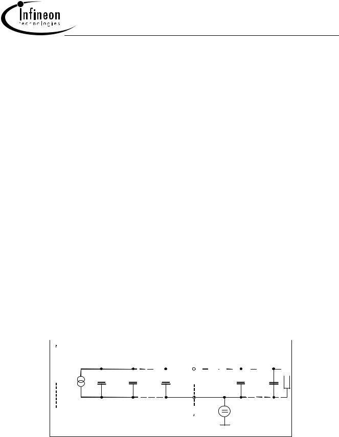
External Heatsink |
|
|
|
||||||||||||||||
|
|
|
|
|
Ptot (t) |
Tj |
|
|
|
Rth1 |
|
|
|
|
|
|
|
|
|
|
|
|
|
|
|
|
|
|
|
|
|
|
|
|
|
|
Rth,n |
|
Tcase |
|
|
|
|
|
||||||||||||||||||||||||||||||||||||||||||||||||||||||
|
|
|
|
|
|
|
|
|
|
|
|
|
|
|
|
|
|
|
|
|
|
|
|
|
|
|
|
|
|
|
|
|
|
|
|
|
|
|
|
|||||||||||||||||||||||||||||||||||||||||||||||||||||||||||
|
|
|
|
|
|
|
|
|
|
|
|
|
|
|
|
|
|
|
|
|
|
|
|
|
|
|
|
|
|
|
|
|
|
|
|
|
|
|
|
|
|
|
|
|
|
|
|
|
|
|
|
|
|
|
|
|
|
|
|
|
|
|
|
|
|
|
|
|
|
|
|
|
|
|
|
|
|
|
|
|
||||||||||||||||||
Cth1 |
Cth2 |
Cth,n |
|
|
Tam b |
|
|
|
|
|
|
|
|
|
|
|
|
|
|
|
|
|
|
|
|
|
|
|
|
|
|
|
|
|
|
|
|
|
|
|
|
|
|
|
|
|
|
|
|
|
|
|
|
|
|
|
|
|
|
|
|
|
|
|
|
|
|
|
|
|
|
|
|
|
|
|
|
|
|
|
|
|
|
|
|
|
|
|
|
|
|
|
|
|
|
|
|
|
|
|
|
|
|
|
|
|
|
|
|
|
|
|
|
|
|
|
|
|
|
|
|
|
|
|
|
|
|
|
|
|
|
|
|
|
|
|
|
|
|
|
|
|
|
|
|
|
|
|
|
|
|
|
|
|
|
|
|
|
|
|
|
|
|
|
|
|
|
|
|
|
|
|
|
|
|
|
|
|
|
|
|
|
|
|
|
|
|
|
|
|
|
|
|
|
|
|
|
|
|
|
|
|
|
|
|
|
|
|
|
|
|
|
|
|
|
|
|
|
|
|
|
|
|
|
|
|
|
|
|
|
|
|
|
|
|
|
|
|
|
|
|
|
|
|
|
|
|
|
|
|
|
|
|
|
|
|
|
|
|
|
|
|
|
|
|
|
|
|
|
|
|
|
|
|
|
|
|
|
|
|
|
|
|
|
|
|
|
|
|
|
|
|
|
|
|
|
|
|
|
|
|
|
|
|
|
|
|
|
|
|
|
|
|
|
|
|
|
|
|
|
|
|
|
|
|
|
|
|
|
|
|
|
|
|
|
|
|
|
|
|
|
|
|
|
|
|
|
|
|
|
|
|
|
|
|
|
|
|
|
|
|
|
|
|
|
|
|
|
|
|
|
|
|
|
|
|
|
|
|
|
|
|
|
|
|
|
|
|
|
|
|
|
|
|
|
|
|
|
|
|
|
|
|
|
|
|
|
|
|
|
|
|
|
|
|
|
|
|
|
|
|
|
|
|
|
|
|
|
|
|
|
Rev.2.1 |
|
|
|
|
|
|
|
|
|
|
|
|
|
|
|
|
|
|
|
|
|
|
|
|
|
|
|
|
|
|
|
|
|
|
|
|
|
|
|
|
|
|
|
|
|
|
|
|
|
|
Page 4 |
2004-09-07 |
||||||||||||||||||

SPP20N60C3, SPB20N60C3 SPI20N60C3, SPA20N60C3
1 Power dissipation
Ptot = f (TC) |
|
|
|
|
|
|
|
||
|
240 |
SPP20N60C3 |
|
|
|
|
|
|
|
|
W |
|
|
|
|
|
|
|
|
|
200 |
|
|
|
|
|
|
|
|
|
180 |
|
|
|
|
|
|
|
|
tot |
160 |
|
|
|
|
|
|
|
|
|
|
|
|
|
|
|
|
|
|
P |
140 |
|
|
|
|
|
|
|
|
|
|
|
|
|
|
|
|
|
|
|
120 |
|
|
|
|
|
|
|
|
|
100 |
|
|
|
|
|
|
|
|
|
80 |
|
|
|
|
|
|
|
|
|
60 |
|
|
|
|
|
|
|
|
|
40 |
|
|
|
|
|
|
|
|
|
20 |
|
|
|
|
|
|
|
|
|
00 |
20 |
40 |
60 |
80 |
100 |
120 |
°C |
160 |
|
|
|
|
|
|
|
|
TC |
|
2 Power dissipation FullPAK
Ptot = f (TC) |
|
|
|
|
|
|
|
|
35 |
|
|
|
|
|
|
|
|
W |
|
|
|
|
|
|
|
|
25 |
|
|
|
|
|
|
|
|
tot |
|
|
|
|
|
|
|
|
P |
|
|
|
|
|
|
|
|
20 |
|
|
|
|
|
|
|
|
15 |
|
|
|
|
|
|
|
|
10 |
|
|
|
|
|
|
|
|
5 |
|
|
|
|
|
|
|
|
00 |
20 |
40 |
60 |
80 |
100 |
120 |
°C |
160 |
|
|
|
|
|
|
|
TC |
|
3 Safe operating area |
4 Safe operating area FullPAK |
ID = f ( VDS ) |
|
|
|
|
parameter : D = 0 , TC=25°C |
|
|
|
|
10 2 |
|
|
|
|
A |
|
|
|
|
10 1 |
|
|
|
|
D |
|
|
|
|
I |
|
|
|
|
10 0 |
|
|
|
|
|
tp = 0.001 ms |
|
|
|
|
tp = 0.01 ms |
|
|
|
|
tp = 0.1 ms |
|
|
|
10 -1 |
tp = 1 ms |
|
|
|
DC |
|
|
|
|
10 -2 |
10 1 |
10 2 |
V |
10 3 |
10 0 |
||||
|
|
|
VDS |
|
Rev.2.1
ID = f (VDS) |
|
|
|
|
parameter: D = 0, TC = 25°C |
|
|
|
|
10 2 |
|
|
|
|
A |
|
|
|
|
10 1 |
|
|
|
|
D |
|
|
|
|
I |
|
|
|
|
10 0 |
|
|
|
|
|
tp = 0.001 ms |
|
|
|
10 -1 |
tp = 0.01 ms |
|
|
|
tp = 0.1 ms |
|
|
|
|
|
tp = 1 ms |
|
|
|
|
tp = 10 ms |
|
|
|
|
DC |
|
|
|
10 -2 |
10 1 |
10 2 |
V |
10 3 |
10 0 |
||||
|
|
|
VDS |
|
Page 5 |
|
2004-09-07 |
||
 Loading...