


 Loading...
TM 11-6625-2809-14 & P
TECHNICAL MANUAL
OPERATOR’S, ORGANIZATIONAL, DIRECT SUPPORT AND GENERAL SUPPORT MAINTENANCE MANUAL (INCLUDING REPAIR PARTS AND SPECIAL TOOLS LISTS) FOR
MULTIMETER ME-498/U (HEWLETT-PACKARD
MODEL 34702A) (NSN 6625-00-538-9794)
AND
INDICATOR ID-2101/U (HEWLETT-PACKARD
MODEL 34750A) (NSN 6625-00-538-9758)
HEADQUARTERS, DEPARTMENT OF THE ARMY
JUNE 1979

TM 11-6625-2809-14 & P
This manual includes copyright material reproduced by permission of the HEWLETT-PACKARD Company.
TECHNICAL MANUAL |
HEADQUARTERS |
|
DEPARTMENT OF THE ARMY |
No.11-6625-2809-14 & P |
Washington, DC 14June1979 |
OPERATOR’S, ORGANIZATIONAL, DIRECT SUPPORT AND
GENERAL SUPPORT MAINTENANCE MANUAL
(INCLUDING REPAIR PARTS AND SPECIAL TOOLS LISTS)
FOR
MULTIMETER ME-4981U (HEWLETT-PACKARD MODEL 34702A) (NSN 6625-00-538-9794)
AND
INDICATOR ID-21011U (HEWLETT-PACKARD MODEL 34750A) (NSN 6625-00-538-9758)
REPORTING OF ERRORS
You can improve this manual by recommending improvements using DA Form 2028-2 located in the back of the manual. Simply tear out the self-addressed form, fill it out as shown on the sample, fold it where shown, and drop it in the mail.
If there are no blank DA Forms 2028-2 in the back of your manual, use the standard DA Form 2028 (Recommended Changes to Publications and Blank Forms) and forward to Commander, US Army Communications and Electronics Materiel Readiness Command, ATTN: DRSEL-ME-MQ, Fort Monmouth, NJ 07703.
In either case a reply will be forwarded direct to you.
This manual is an authentication of the manufacturer’s commercial literature which, through usage, has been found to cover the data required to operate and maintain this equipment. Since the manual was not prepared In accordance with military specifications and AR 310-3, the format has not been structured to consider levels of maintenance.
i
Table of Contents |
TM 11-6625-2809-14 & P |
TABLE OF CONTENTS
PART ONE
Section |
|
|
Page |
0. |
INTRODUCTION........................................ |
0-1 |
|
I. |
GENERAL INFORMATION ........................ |
1-1 |
|
|
1-1. |
Description .................................... |
1-1 |
|
1-6. |
Specifications ................................ |
1-3 |
|
1-8. |
Options .......................................... |
1-3 |
|
1-10. |
Accessories Available |
|
|
|
(See Figure 1-2) ............................ |
1-3 |
|
1-11. |
Instrument and Manual |
|
|
|
Identification ................................. |
1-3 |
Section |
|
|
Page |
II. |
INSTALLATION.......................................... |
2-1 |
|
|
2-1. |
Introduction ................................... |
2-1 |
|
2-3. |
Initial Inspection............................. |
2-1 |
|
2-5. |
Power Requirements .................... |
2-1 |
|
2-7. |
Grounding Requirements .……….2-2 |
|
|
2-10. |
Environmental Requirements .……2-2 |
|
|
2-12. |
Instrument Mounting ..................... |
2-2 |
|
2-13. |
Bench Use .………… . ................... |
2-2 |
|
2-15. |
Rack Use ...................................... |
2-2 |
|
2-17. |
Repackaging for Shipment .… . ..... |
2-2 |
|
2-21. |
Power Cords and Receptacles .… .2-3 |
|
Section |
|
|
Page |
III. |
OPERATING INSTRUCTIONS |
..................3-1 |
|
|
3-1. |
Introduction.................................... |
3-1 |
|
3-3. |
Rear Panel Features ..................... |
3-1 |
|
3-5. Warm-Up ....................................... |
3-1 |
|
|
3-7. |
Operation with Plug-On ..Modules 3-1 |
|
Section |
|
|
Page |
|
IV. |
THEORY OF OPERATION |
...........4-1 |
4-1. |
Introduction................................................. |
4-1 |
|
4-3. |
Basic Measurement Sequence .................. |
4-1 |
|
4-5. |
Analog Circuits ........................................... |
4-1 |
|
4-4. |
Input Amplifier ............................................ |
4-1 |
|
4-8. |
Integrator .................................................... |
4-2 |
|
4-10. |
Zero Detect Circuits.................................... |
4-2 |
|
4-12. |
Auto-Zero Cycle.......................................... |
4-2 |
|
4-14. |
Digital Processing Circuits.......................... |
4-2 |
|
4-17. |
Data Clock (Refer to |
|
|
|
Figure 4-8).................................................. |
4-4 |
|
4-19. |
Timing Generator Circuit (See |
|
|
|
Figure 7-8).................................................. |
4-4 |
|
4-21. |
Zero Detect and Data Transfer |
|
|
|
(Refer to Figure 4-10)................................. |
4-4 |
|
4-23. |
Data Accumulator and Storage |
|
|
|
(Refer to Figure 7-7)................................... |
4-6 |
|
Section |
|
Page |
4-25. |
Data Display and Control Circuits |
|
|
(Refer to Figure 4-11) .…… . ...................... |
4-6 |
4-27. |
Reset Timing (See Figure 4-12) ................ |
4-7 |
4-29. |
Least Significant Digit Blank |
|
|
(Refer to Figure 7-8) .…… . ........................ |
4-7 |
Section |
|
Page |
V. |
MAINTENANCE ........................................ |
5-1 |
5-1. |
Introduction ............................................... |
5-1 |
5-3. |
Operational Checks .................................. |
5-1 |
5-6. |
Adjustment Procedures.............................. |
5-1 |
5-8. |
Cover Removal .......................................... |
5-2 |
5-10. |
Adjustment Locator ................................... |
5-2 |
5-12. |
Power Supply Adjustment .… .................... |
5-2 |
5-13. |
Input Amp. Offset Adjustment … … ............ |
5-2 |
5-14. |
Zero Detect Comparator Offset … . ............ |
5-2 |
5-15. |
Zero Detect Hysteresis |
|
|
Adjustment .……… … ................................. |
5-2 |
5-16. |
Reference Voltage Adjustments … ............ |
5-3 |
Section |
|
Page |
VI. |
IDENTIFICATION OF PARTS |
.................. 6-1 |
6-1. |
Introduction .………… ................................ |
6-1 |
6-4. |
Deleted |
|
6-6. |
Deleted |
|
6-8. |
Proprietary Parts .…………… . .................... |
6-1 |
Section |
|
Page |
VII. |
CIRCUIT DIAGRAMS AND |
|
|
TROUBLESHOOTING .……… . ................. |
7-1 |
7-1. |
Introduction .………… ................................ |
7-1 |
7-3. |
Troubleshooting .……… . ........................... |
7-1 |
7-4. |
Troubleshooting Trees .…… ...................... |
7-1 |
7-6. |
Troubleshooting Procedures ..................... |
7-1 |
7-8. |
Functional Block Diagram |
|
|
(Figure 7-4) .……… . .................................. |
7-1 |
7-10. |
Timing Circuits (Figure 7-5) ...................... |
7-1 |
7-12. |
Schematic Diagrams (Figures |
|
|
7-6, 7-7 and 7-8) .…… . .............................. |
7-1 |
7-14. |
Component Location Diagrams ................ |
7-1 |
APPENDIXES |
|
|
A. |
Difference Data Sheet ............................... |
A-1 |
B. |
References ................................................ |
B-1 |
C. |
Maintenance Allocation .……………… |
… .. C-1 |
D.Repair Parts And Special
Tools List................................................... |
D-1 |
ii
Table of Contents |
TM 11-6625-2809-14 & P |
|
LIST OF TABLES |
|
Table |
|
Page |
1-1. |
Specifications ................................................ |
1-2 |
1-2. |
General Information ...................................... |
1-3 |
3-1. |
34721B/5055A Output Codes ....................... |
3-1 |
5-1. |
Recommended Test Equipment ................... |
5-1 |
5-2. |
DC Accuracy ................................................. |
5-2 |
5-3(a). |
AC Accuracy (45 Hz and 20 kHz................... |
5-5 |
5-3(b). |
AC Accuracy (100 kHz)................................. |
5-6 |
5-4. |
Accuracy Test .............................................. |
5-7 |
6-1. |
Identification of Parts..................................... |
6-3 |
|
LIST OF ILLUSTRATIONS |
|
Figure |
|
Page |
1-1 |
Instrument Serial Number ............................ |
1-1 |
2-1. |
Installation of the Model 34702A.................. |
2-1 |
3-1. |
Front add Rear Panel Features.................... |
3-0 |
4-1. |
Block Diagram.............................................. |
4-0 |
4-2. |
ACV/DCV Attenuator.................................... |
4-1 |
4-3. |
W Converter ................................................. |
4-2 |
4-4. |
AC/DC Converter ......................................... |
4-3 |
4-5. |
Impedance Converter................................... |
4-4 |
5-1. |
Input Impedance Test .................................. |
5-3 |
5-2. |
Effective Common Mode Rejection.............. |
5-3 |
5-3. |
Normal Mode Rejection................................ |
5-4 |
5-4. |
Removal from Case ..................................... |
5-8 |
5-5. |
Adjustment Locator ...................................... |
5-9 |
7-1. |
AC Converter Troubleshooting Tree ............ |
7-3/7-4 |
7-2. |
W Converter Troubleshooting Tree.............. |
7-3/7-4 |
7-3. |
34702A Schematic ....................................... |
7-5/7-6 |
iii
TM 11-6625-2809-14 & P
TABLE OF CONTENTS
PART TWO
Section |
|
|
Page |
I. |
GENERAL INFORMATION ........................ |
1-1 |
|
|
1-1. |
Description .................................... |
1-1 |
|
1-6.Specifications ....................................... |
1-3 |
|
|
1-8. |
Options .......................................... |
1-3 |
|
1-10. |
Accessories Available |
|
|
|
(See Figure 1-2) ........................... |
1-3 |
|
1-11. |
Instrument and Manual |
|
|
|
Identification .…… … ..................... |
1-3 |
Section |
|
|
Page |
II. |
INSTALLATION ......................................... |
2-1 |
|
|
2-1. |
Introduction.................................... |
2-1 |
|
2-3. |
Initial Inspection............................. |
2-1 |
|
2-5. |
Power Requirements..................... |
2-1 |
|
2-7. |
Grounding Requirements .............. |
2-2 |
|
2-10. |
Environmental Requirements ........ |
2-2 |
|
2-12. |
Instrument Mounting...................... |
2-2 |
|
2-13. |
Bench Use..................................... |
2-2 |
|
2-15. |
Rack Use....................................... |
2-2 |
|
2-17. |
Repackaging for Shipment ............ |
2-2 |
|
2-21. |
Power Cords and Receptacles...... |
2-3 |
Section |
|
|
Page |
III. |
OPERATING INSTRUCTIONS |
..................3-1 |
|
|
3-1. |
Introduction.................................... |
3-1 |
|
3-3. |
Rear Panel Features ..................... |
3-1 |
|
3-5. Warm-Up ....................................... |
3-1 |
|
|
3-7. |
Operation with Plug-On Modules .3-1 |
|
Section |
|
Page |
4-25. |
Data Display and Control Circuits |
|
|
(Refer to Figure 4-11) ................... |
4-6 |
4-27. |
Reset Timing (See Figure4-12).................. |
4-7 |
4-29. |
Least Significant Digit Blank |
|
|
(Refer to Figure 7-7) .................................. |
4-7 |
Section |
|
Page |
V. |
MAINTENANCE......................................... |
5-1 |
5-1. |
Introduction ................................................ |
5-1 |
5-3. |
Operational Checks .................................. |
5-1 |
5-6. |
Adjustment Procedures.............................. |
5-1 |
5-8. |
Cover Removal ......................................... |
5-2 |
5-10. |
Adjustment Locator .................................... |
5-2 |
5-12. |
Power Supply Adjustment.......................... |
5-2 |
5-13. |
Input Amp. Offset Adjustment ................... |
5-2 |
5-14. |
Zero Detect Comparator Offset ................ |
5-2 |
5-15. |
Zero Detect Hysteresis |
|
|
Adjustment ................................................. |
5-2 |
5-16. |
Reference Voltage Adjustments . .............. |
5-3 |
Section |
|
Page |
VI. |
IDENTIFICATION OF PARTS |
................... 6-1 |
6-1. |
Introduction ................................................ |
6-1 |
6-4. |
Deleted |
|
6-6. |
Deleted |
|
6-8. |
Parts Changes ........................................... |
6-1 |
Section |
|
|
Page |
IV. |
THEORY OF OPERATION ........................ |
4-1 |
|
|
4-1. |
Introduction.................................... |
4-1 |
|
4-3. |
Basic Measurement Sequence . ... |
4-1 |
|
4-5. |
Analog Circuits .............................. |
4-1 |
|
4-6. |
Input Amplifier ............................... |
4-1 |
|
4-8. |
Integrator ....................................... |
4-2 |
|
4-10. |
Zero Detect Circuits....................... |
4-2 |
|
4-12. |
Auto-Zero Cycle............................. |
4-2 |
|
4-14. |
Digital Processing Circuits............. |
4-2 |
|
4-17. |
Data Clock (Refer to |
|
|
|
Figure 4-8)..................................... |
4-4 |
|
4-19. |
Timing Generator Circuit (See |
|
|
|
Figure 7-8)..................................... |
4-4 |
|
4-21. |
Zero Detect and Data Transfer |
|
|
|
Circuits (Refer to Figure 4-10)....... |
4-4 |
|
4-23. |
Data Accumulator and Storage |
|
|
|
(Refer to Figure 7-7)...................... |
4-6 |
6-10. |
Proprietary Parts................................ |
6-1 |
Section |
|
Page |
VII. |
CIRCUIT DIAGRAMS AND |
|
|
TROUBLESHOOTING............................... |
7-1 |
7-1. |
Introduction ................................................ |
7-1 |
7-3. |
Troubleshooting ......................................... |
7-1 |
7-4. |
Troubleshooting Trees ............................... |
7-1 |
7-6. |
Troubleshooting Procedures...................... |
7-1 |
7-8. |
Functional Block Diagram |
|
|
(Figure 7-4) ................................................ |
7-1 |
7-10. |
Timing Circuits (Figure 7-5) ....................... |
7-1 |
7-12. |
Schematic Diagrams (Figures |
|
|
7-6, 7-7 and 7-8) ........................................ |
7-1 |
7-14. |
Component Location Diagrams ................. |
7-1 |
Appendix |
Page |
|
A. |
Difference Data Sheet................................. |
A-1 |
iv
TM 11-6625-2809-14 & P
Table of Contents
LIST OF ILLUSTRATIONS
Figure |
|
Page |
1-1. |
Plug-On Modules which can be used |
|
|
with the 34750A Display Module ................ |
1-1 |
1-2. |
Accessories Available for use with 34750A.. 1-2 |
|
1-3. |
Instrument Serial Number (on rear panel) .1-3 |
|
2-1. |
Voltage Selection........................................ |
2-1 |
2-2. |
Rick Mount Kits .......................................... |
2-2 |
2-3. |
Power Receptacles .................................... |
2-3 |
3-1. |
34750A Rear Panel .................................... |
3-1 |
4-1. |
Basic Block Diagram of 34750A................. |
4-0 |
4-2. |
Simplified Diagram of the |
|
|
Input Amplifier ............................................ |
4-1 |
4-3. |
Simplified Diagram of the |
|
|
Integrator Circuit......................................... |
4-2 |
4-4. |
Simplified Diagram of Zero Detect |
|
|
Circuits ...................................................... |
4-2 |
4-5. |
34750A Circuits shown in Auto-Zero |
|
|
Mode ...................................................... |
4-3 |
4-6. |
Block Diagram of Typical ASM................... |
4-3 |
4-7. |
ASM Simplified Block Diagram................... |
4-4 |
4-8. |
Data Clock.................................................. |
4-4 |
Figure |
|
Page |
4-9. |
34750A Flow Chart .................................... |
4-5 |
4-10. |
Zero Detect and Data Transfer |
|
|
Timing ...................................................... |
4-6 |
4-11. |
Data Display Circuits.................................. |
4-6 |
4-12. |
Reset Tuning ............................................. |
4-7 |
5-I. |
11456A Readout Test Card ....................... |
5-1 |
5-2. |
Cover Removal .......................................... |
5-2 |
5-3. |
Zero Detect Comparator Offset |
|
|
Adjustment ................................................. |
5-2 |
5-4. |
Chassis Mounted Component and |
|
|
Adjustment Locator .................................... |
5-3 |
7-1. |
Power Supply Troubleshooting |
|
|
Tree ................................................ |
7-3/7-4 |
7-2. |
Analog Troubleshooting Tree..................... |
7-5 |
7-3. |
Digital Troubleshooting Tree................ |
7-7/7-8 |
7-4. |
Functional Block Diagram .................. |
7-9/7-10 |
7-5. |
Timing Waveforms ........................... |
7-11/7-12 |
7-6. |
Analog Signal Processor.................. |
7-13/7-14 |
7-7. |
Digital Signal Processor................... |
7-15/7-16 |
7-8. |
Power Supply ................................... |
7-17/7-18 |
|
LIST OF TABLES |
|
Table |
|
Page |
1-1. |
3470A Series Signal Conditioning |
|
|
Modules ......................................................... |
1-3 |
1-2. |
Available Options .............................................. |
1-3 |
5-1. |
Recommended Test Equipment ....................... |
5-1 |
5-2. |
Operational Checks .......................................... |
5-1 |
6-1. |
Identification of Parts ........................................ |
6-2 |
7-1. |
Troubleshooting Trees ...................................... |
7-1 |
v

TM 11-6625-2809-14 & P
hp
PART ONE
OPERATING AND SERVICE MANUAL
Binder part No. 34740-90011 (Includes cover sheet)
Manual Part No. 34740-90012 or 34750-90012 (Binder, System Introduction and Display Manual)
MODEL 3470
MEASUREMENT SYSTEM
IMPORTANT NOTICE
This instruction manual requires no change sheet. Any change information has already been integrated into the manual by page revisions. Revised pages have a revision letter which can be found on the lower corner of the page. Reference may also be made to Section VIII of each manual where backdating information for earlier instruments can be found.
Copyright Hewlett-Packard Company 1972
P.O. Box 301, Loveland, Colorado 80537 U.S.A.
Printed: June 1973
vi

TM 11-6625-2809-14 & P
|
hp |
HEWLETT |
PACKARD |
CERTIFICATION
Hewlett-Packard Company certifies that this instrument met its published specifications at the time of shipment from the factory. Hewlett-Packard Company further certifies that its calibration measurements are traceable to the United States National Bureau of Standards, to the extent allowed by the Bureau’s calibration facility, and to the calibration facilities of other International Standards Organization members.
WARRANTY AND ASSISTANCE
This Hewlett-Packard product is warranted against defects in materials and workmanship for a period of one year from the date of shipment, except that in the case of certain components, if any, listed in Section I of this operating manual, the warranty shall be for the specified period. Hewlett-Packard will, at its option, repair or replace products which prove to be defective during the warranty period provided they are returned to Hewlett-Packard, and provided the proper preventive maintenance procedures as listed in this manual are followed. Repairs necessitated by misuse of the product are not covered by this warranty. NO OTHER WARRANTIES ARE EXPRESSED OR IMPLIED, INCLUDING BUT NOT LIMITED TO THE IMPLIED WARRANTIES OF MERCHANTABILITY AND FITNESS FOR A PARTICULAR PURPOSE. HEWLETT-PACKARD IS NOT LIABLE FOR CONSEQUENTIAL DAMAGES.
If this product is sold as part of a Hewlett-Packard integrated instrument system, the above warranty shall not be applicable, and this product shall be covered only by the system warranty.
Service contracts or customer assistance agreements are available for Hewlett-Packard products.
For any assistance, contact your nearest Hewlett-Packard Sales and Service Office, Addresses are provided at the back of this manual.
vii
TM 11-6625-2809-14 & P
INTRODUCTION
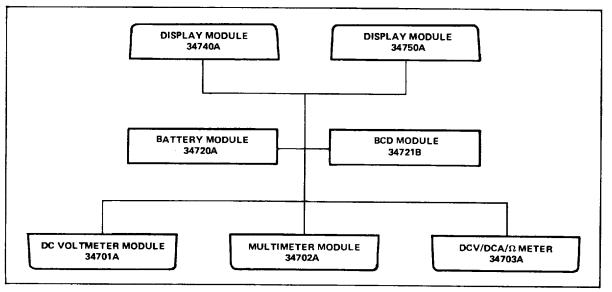
The 3470 Measurement System is a series of modules that may be plugged together to form several different measuring instruments, including both line powered and battery powered versions.
A mainframe display module is connected to a bottom plug-on function module to form a complete instrument.
The BCD and/or Battery plug-on module may be added between the display and function modules as desired.
Refer to the Operating and Service Manual of the plugon module to be used with the display module for the operating instructions, incoming inspection, and adjustment procedures of the instrument as a whole.
Possible Instrument Configurations
viii
TM 11-6625-2809-14 & P
SECTION 0
INTRODUCTION
0-1. SCOPE.
a.This manual in Part 1, describes Multimeter ME-498/U (fig. 3-1) and provides instructions for operation and maintenance. Throughout this manual the ME-498/U is referred to as the Hewlett-Packard Model 34702A.
b.Part 2 describes Indicator ID-2101/U (fig.1-1, Part 2). This display module is referred to as the Hewlett-Packard Model 34750A.
0-2. INDEXES OF PUBLICATIONS.
a.DA Pam 310-4. Refer to the latest issue of DA Pam 310-4 to determine whether there are new editions, changes, or additional publications pertaining to the equipment.
b.DA Pam 310-7. Refer to DA Pam 310-7 to determine whether there are modification work orders (MWO’s) pertaining to the equipment.
0-3. FORMS AND RECORDS.
a.Reports of Maintenance and Unsatisfactory Equipment. Maintenance forms, records, and reports which are to be used by maintenance personnel at all maintenance levels are listed in and prescribed by TM 38-750.
b.Report of Packaging and Handling Deficiencies. Fill out and forward DD Form 6 (Packaging
Improvement Report) as prescribed in AR 70058/NAVSUPINST 4030.29/AFR 71-13/MCOP40 30.29A and DLAR 4145.8.
c. Discrepancy in Shipment Report (DISREP) (SF 361). Fill out and forward Discrepancy in
Shipment Report (DISREP) (SF 361) as prescribed in AR 55-38/NAVSUPINST 4610.33B/AFR 7518/MCO P4610.19C and DLAR 4500.15.
0-4. REPORTING EQUIPMENT
IMPROVEMENT RECOMMENDATIONS (EIR).
EIR’s will be prepared using SF 368 (Quality Deficiency Report). Instructions for preparing EIR’s are provided in TM 38-750, the Army Maintenance Management System. EIR’s should be mailed direct to Commander, US Army Communication and Electronics Materiel Readiness Command, ATTN: DRSEL-ME-MQ, Fort Monmouth, NJ A reply will be furnished direct to you.
0-5. ADMINISTRATIVE STORAGE.
Administrative storage of equipment issued to and used by Army activities shall be in accordance with TM 740- 90-1 and paragraph 2-8.
0-6. DESTRUCTION OF ARMY ELECTRONICS MATERIEL.
Destruction of Army electronics materiel to prevent enemy use shall be in accordance with TM 750-244-2.
0-1
Model 34702A |
TM 11-6625-2809-14 & P |
SECTION I
GENERAL INFORMATION
1-1. INTRODUCTION.
1-2. This manual contains installation and operating instructions as well as maintenance information which includes performance checks for the Model 34702A. A schematic diagram, theory of operation, and troubleshooting information are provided for use in maintaining the 34702A Multimeter Module.
1-3. DESCRIPTION.
1-6. Table 1-1 lists specifications for the Model 34702A Multimeter. This table supersedes all other previously printed specifications. Procedures are provided in Section V to verify performance of the instrument to its specifications and to readjust the instrument if required. The accuracy specifications apply for ambient temperatures of 230C+ 50C. For temperatures outside this range, a temperature coefficient factor (listed in Table 1-1) must be used.
1-7. Table 1-2 lists general information relating to the instrument.
1-4. The Hewlett-Packard Model 34702A Multimeter is a signal conditioning module that may be connected to a Model 34740A or 34750A Display Module, to measure AC Voltage, DC Voltage, or resistance. The AC and DC volts functions provide four decade ranges from I V to 1000 V. Six resistance ranges from 100 full scale to 10 MQ full scale are provided by the "Ω (fy)" function. Each available range of the Model 34702A has 100% overranging capability except the 1000 V range which has 20%.
Overload protection circuits allow up to 1200 V peak to be applied to the INPUT V terminals without damaging the instrument. Up to 350 V can be applied to the INPUT S terminals without damaging the instrument. No more than 500 V should be applied between LO and Chassis. Do not apply voltage between LO and Chassis when using the 34721A or 34721B BCD Module. These modules connect LO to Chassis when attached to the Model 34 702A.
1-8. INSTRUMENT AND MANUAL IDENTIFICATION.
1-9. A three-section serial number (xxxxAxxxxx) is used to identify your Model 34702A. Figure 1-1 illustrates the meaning of the three parts of the number.
1-10. This manual is kept up-to-date with revised pages. If the serial number of your instrument is lower than the one on the title page of this manual, refer to the backdating information in Appendix A which adapts this manual to your instrument. All correspondence with Hewlett-Packard Company should include the complete serial number.
1-5. SPECIFICATIONS AND GENERAL |
Figure 1-1. Instrument Serial Number. |
INFORMATION. |
|
|
1-1 |

Model 34702A |
TM 11-6625-2809-14 & P |
Table 1-1. Specifications. (Measured using 34740A or 34750A Display Unit)
DC VOLTAGE 34740A
Performance:
Accuracy (+ 230C t 50C), < 95% RH)
30 days |
+ (0.03% of reading + .01% of range) |
|
90 days |
+ (0.04% of reading + .01% of range) |
|
6 |
mo. |
+ (0.05% of reading + .02% of range) |
1 |
yr. |
+ (0.06% of reading + .02% of range) |
Stability (24 hours, + 230C + 1°C)
+ (0.01% of reading + 0.005% of range)
Temperature Coefficient (00 C to + 500C)
DC voltage: t (0.0035% of reading + 0.001% of range)/oC.
Input Characteristics: Input resistance
1 and 10 V ranges: 11.11 M + 0.2%
100 V range: 10.1 M + 0.2%
1000 V range: 10 M + 02%
Effective Common Mode Rejection (1 k unbalance) DC: > 80 dB.*
Normal Mode Rejection
50 Hz (Option 050): >60dB (50 Hz + 0.1%)
60 Hz (Option 060): >60dB (60 Hz + 0.1%)
*Does not apply when BCD Module is used.
AC VOLTAGE 34740A
Performance:
Accuracy (+ 23°C + 5 0C, <95% RH) 30 days
45 Hz to 20 kHz + (0.25% of reading + .05% of range)
20 kHz to 100 kHz + (0 75% of reading + .05% of range)
90 days
45 Hz to 20 kHz + (0.30% of reading + .05% of range)
20 kHz to 100 kHz + (0.80% of reading + .05% of range)
6mo.
45 Hz to 20 kHz + (0.35% of reading + .05% of range)
20 kHz to 100 kHz + (085% of reading + .05% of range)
+ (0.50% of reading + 0.05% of range)
20 kHz to 100 kHz + (1.0% of reading + 0.05% of range)
Temperature Coefficient (0°C to + 50 0C)
AC voltage: ± (0,03% of reading + 0.001% of range) /0C.
Stability (24 hours, + 23°C + 1°C)
AC voltage: 45 Hz to 20 kHz: ± (0.15% of reading + 0.05% of range)
20 kHz to 100 kHz: + (0.4% of reading + 0.05% of range)
Response Time: < 2 s within + 0.3% of final value or 20 counts, whichever is greater.
Input Characteristics:
Input impedance
1 and 10 V ranges: 11.11 M + 02%/ /80 pF max. 100 V range: 10.1 M ± 0.2%/ /80 pF max.
1000 V range: 10 M + 0.2%/180 pF max.
OHMS 34740A
Performance:
Accuracy (+ 230C ± 50C,< 95% RH) 30 days
10 MO range + (0.25% of reading + 0.02% of range)
All other ranges + (0.05% of reading + 0.02% of range)
+ (0.30% of reading + 0.02% of range)
All other ranges + (0.06% of reading + 0.02% of range)
+ (0.35% of reading + 0.03% of range)
All other ranges + (0.07% of reading + 0.03% of range)
± (0.50% of reading + 0.03% of range)
All other ranges t (0.11% of reading + 0.03% of range)
Stability (24 hours, 23°C + 1 0C)
10 Mn range + (0.1% of reading + 0.01% of range)
All other ranges + (0.02% of reading + 0.02% of range)
Temperature Coefficient (00C to + 500C)
Ω
10 Ml range: + (0.035% of reading + 0.001% of range) / C.
All other ranges' t (0.006% of reading + 0.001% of range) / C.
DC VOLTAGE 34750A
Performance:
Accuracy (+ 23°C + 5 0C), < 95% RH)
30 days |
± (0.025% of reading + .005% of range) |
90 days |
+ (0.035% of reading + .005% of range) |
6 mo. |
+ (0.045% of reading + .007% of range) |
1 yr. |
+ (0.06% of reading + .01% of range) |
NOTE: Due to temperature change inside the instrument between line and battery operation, the references must be adjusted when changing modes to achieve these specifications
Stability (24 hours, + 230C + 10C)
DC voltage: + (.008% of reading i .004% of range) Temperature Coefficient (0°C to + 50 0C)
DC voltage: ± (0.0025% of reading + 0.0002% of range) / C
Input Characteristics Input resistance
1 and 10 V ranges: 11.11 M + 0.2%
100 V range: 10.1 M +.0.2%
1000 V range: 10 M + 0.2%
Effective Common Mode Rejection (1 kO unbalance) DC: >80 dB.*
*Does not apply when BCD Module is used
Rev. A 1-2

Model 34702A |
TM 11-6625-2809-14 & P |
Table 1-1. Specifications (Cont’d).
Normal Mode Rejection
50 Hz (Option 050): >60 dB (50 Hz + 0.1%) 60 Hz (Option 060): >60 dB (60 Hz + 0.1%)
AC VOLTAGE 34750A
Performance:
Accuracy (+ 230 + 5C, A 95% RH) 30 days
45 Hz to 20 kHz +(0.25% of reading + .05% of range)
20 kHz to 100 kHz + (.75% of reading + .05% of range)
+ (.3% of reading + .05% of range)
20 kHz to 100 kHz + (.8% of reading + .05% of range)
± (.35% of reading + .05% of range)
20 kHz to 100 kHz + (.85% of reading + .05% of range)
+ (0.50% of reading + 0.05% of range)
20 kHz to 100 kHz ± (1.0% of reading + 0.05% of range)
Stability (24 hours, + 230C ± 10 C)
AC voltage: 45 Hz to 20 kHz: + (0.15% of reading + 0.05% of range)
20 kHz to 100 kHz: + (0.4% of reading + 0.05% of range)
Temperature Coefficient (0oC to + 50°C)
AC voltage: + (0.03% of reading + 0.001% of range) /°C
Response Time: < 2 s within + 0.3% of final value or 200 counts, whichever is greater.
Input Characteristics: Input impedance
1 and 10 V ranges: 11.11 M + 0.2%/1 /80 pF max. 100 V range: 10.1 M + 0.2%1/80 pF max.
1000 V range: 10 M + 0.2%/ /80 pF max.
OHMS 34750A
Performance:
Accuracy (+ 23oC + 5°C, < 95% RH) 30 days
10 M range ±(0.25% of reading + 0.015% of range)
All other ranges + (0.045% of reading + 0.015% of range)
± (0.3% of reading + 0.015% of range)
All other ranges + (0.055% of reading + 0.015% of range)
± (0.35% of reading + 0.02% of range)
All other ranges + (0.065% of reading + 0.02% of range)
± (0.50% of reading + 0.02% of range)
All other ranges + (0.11% of reading + 0.02% of range)
NOTE: Due to temperature change inside the instrument between line and battery operation, the references must be adjusted when changing modes to achieve these specifications.
Stability (24 hours, 23°C ± 1oC)
10 M range + (0.1% of reading + 0.009% of range) All other ranges + (0.2% of reading + 0.015% of range)
Temperature Coefficient (0o C to + 50o C)
10 M range: ± (0.035% of reading + 0.001% of range) /°C
All other ranges: +(0.006% of reading + 0.001% of range) /oC
|
|
|
|
Table 1-2. General Information. |
|
|
|
|
|
||||||
|
|
|
|
|
|
|
|
|
|
|
|
|
|
|
|
DC VOLTAGE |
|
|
|
Input Characteristics: |
|
|
|
|
|
||||||
|
|
|
|
|
|
|
|
|
|
|
|
||||
34740A |
|
|
|
|
|
Input terminals: floating pair.* |
|
|
|
|
|
||||
Ranges: |
|
|
|
|
|
Maximum input voltage |
|
|
|
|
|
||||
|
|
|
|
|
|
|
|
|
|
|
|
||||
|
|
|
Full Scale |
Maximum |
|
|
High to low 1200 V |
|
|
|
|
|
|||
Range |
|
Reading |
Reading |
|
|
Low to Chassis + 500V* |
|
|
|
|
|
||||
|
|
|
|
|
|
|
*Does not apply when BCD Module is used. |
|
|
||||||
|
1 V |
|
± 1.0000 V |
± 1.9999 V |
|
|
|
||||||||
|
|
|
|
|
|
|
|
|
|
|
|
||||
|
10 V |
|
± 10.000 V |
± 19.999 V |
|
|
AC VOLTAGE |
|
|
|
|
|
|||
100 V |
|
± 100.00 |
±199.99 V |
|
|
|
|
|
|
|
|
|
|
||
1000 V |
|
+ 1.0000 V |
±1200.0 V |
|
|
34740A |
|
|
|
|
|
||||
Overrange |
|
|
|
|
|
|
|
|
|
|
|
|
|
||
1000 |
V range: 20%. |
|
|
|
Ranges: |
|
|
|
|
|
|||||
|
All other ranges: 100% (19999 max reading) |
|
|
|
|
|
|
|
|
|
|
||||
|
|
|
|
|
|
|
|
|
|
||||||
Range Selection: manual pushbuttons |
|
|
|
|
|
|
|
Full Scale |
|
|
Maximum |
|
|||
Performance: |
|
|
|
|
Range |
|
|
Reading |
|
|
Reading |
|
|||
|
|
|
|
1 V |
|
|
1.0000 V |
|
|
1.9999 V |
|
||||
Reading Rate |
|
|
|
|
10 V |
|
|
10.000 V |
|
|
19.999 V |
|
|||
|
|
|
|
100 V |
|
|
100.001 |
|
|
199.99 V |
|
||||
|
Option 050 (50 Hz): 8/s fixed |
|
|
|
|
1000 V |
|
|
1.0000 V |
|
|
1200.0 V |
|
||
|
|
|
|
|
|
|
|||||||||
|
Option 060 (60 Hz): 5/s fixed |
|
|
|
|
|
|
|
|
|
|
|
|
||
|
|
|
|
|
|
|
|
|
|
|
|
|
|
|
|
Rev. A 1-3

Model 34702A |
TM 11-6625-2809-14 & P |
Table 1-2. General Information (Cont’d).
Overrange
1000 V range: 20%
All other ranges: 100% (19999 max reading)
Range selectionmanual pushbuttons
Performance:
Frequency range: 45 Hz to 100 kHz
Input Characteristics:
input terminals: floating pair. * Maximum input voltage
High to low: 1200 V rms. Except 1 V range. 1 V Range:
1200 V rms maximum 45 Hz - 200 Hz
300 V rms maximum 200 Hz - 100 kHz
Low to Chassis: + 500 V *
* Does not apply when BCD Module is used.
Ω
34740A
Ranges:
|
Range |
Full Scale |
|
Maximum |
|
|
|
Reading |
Reading |
|
|||
|
|
|||||
|
|
|
|
|
|
|
|
100 Ω |
100.00 Ω |
199.99 Ω |
|
||
|
1 |
κΩ |
1.0000 ΚΩ |
1.9999 ΚΩ |
|
|
|
10 |
κΩ |
10.000 ΚΩ |
19.999 ΚΩ |
|
|
|
|
|||||
|
100 |
κΩ |
100.00 ΚΩ |
199.99 ΚΩ |
|
|
|
|
|||||
|
1000 |
κΩ |
1000.0 ΚΩ |
1999.9 ΚΩ |
|
|
|
|
|||||
|
10 ΜΩ |
10.000 ΜΩ |
19.999 ΜΩ |
|
||
|
|
|||||
Overrange: 100% on all ranges
Range selection: manual pushbuttons
Input Characteristics:
Input terminals: floating pair (different from voltage input terminals).
Current through measured resistor: 10 mA on 100 Ω range decreasing one decade per successively higher range.
Effective Common Mode Rejection: same as dc specifications.
Overload protection: + 350 V peak (248 V rms sine wave).
Other:
Operating temperature: 0°C to + 50°C.
Storage temperature: - 40oC to + 75oC.
Line requirements: 100/120/220/240 V - 10%, + 5% switchable:
48 Hz to 440 Hz; < 8.7 VA.
DC VOLTAGE 34750A
Ranges:
|
|
|
|
|
|
Full Scale |
|
Maximum |
|
|
Range |
Reading |
Reading |
|
|||||
|
1 |
V |
|
|
+ 1.00000 V |
+ 1.99999 V |
|
||
|
10 |
V |
+ 10.0000 V |
+ 19.9999 V |
|
||||
|
|||||||||
|
100 |
V |
+ 100.000 V |
+ 199.999 V |
|
||||
|
|||||||||
|
!000 V |
+ 1000.00 V |
+ 1200.00 V |
|
|||||
|
|||||||||
|
|
|
|
|
|
|
|
|
|
Overrange
1000V range: 20%
All other ranges 100% (199999 max reading)
Range selection: manual pushbuttons
Reading rate
Option 050 (50 Hz): 4/s fixed
Option 060 (60 Hz). 5/s fixed
Input terminals: floating pair *
Maximum Input voltage High to Low: + 1200 V
Low to Chassis: + 500 V·*
* Does not apply when BCD Module is used.
AC VOLTAGE 34750A
Ranges:
|
|
|
|
|
Full Scale |
|
|
Maximum |
|
|
Range |
|
Reading |
|
Reading |
|
|||
|
1 |
V |
|
1.00000 V |
|
1.99999 V |
|
||
|
10 |
V |
|
10.0000 V |
|
19.9999 V |
|
||
|
100 |
V |
|
100.000 V |
|
199.999 V |
|
||
|
1000 |
V |
|
1000.00 V |
|
|
1200.00 V |
|
|
Overrange
1000 V range: 20%
All other ranges. 100% (199999 max reading)
Range selection: manual pushbuttons
Frequency range: 45 Hz to 100 kHz
Input terminals: floating pair
Maximum input voltage
High to Low: 1200 V rms except on 1 V range. On 1 V range 2.5 x 10⁵ V Hz limit with minimum protection of 300 V rms.
Low Chassis: + 500 V
Ω |
|
|
|
|
34750A |
|
|
|
|
Ranges: |
Ω |
|
100.000 Ω |
199.99 Ω |
100 |
|
|||
|
1 |
κΩ |
1.00000 κΩ |
1.99999 κΩ |
|
10 |
κΩ |
10.0000 κΩ |
19.9999 κΩ |
100 |
κΩ |
100.000 κΩ |
199.999 κΩ |
|
1000 |
κΩ |
1000.00 κΩ |
1999.99 κΩ |
|
10 ΜΩ |
10.0000 ΜΩ |
19.9999 ΜΩ |
||
Overrange: 100% on all ranges
Range: selection manual pushbuttons
Input terminals: floating pair (different from voltage input terminals).
Current through measured resistor: 10 mA on 100 Ω range decreasing one decade per successively higher range.
Effective Common Mode Rejection: same as dc specifications.
Overload protection- t 350 V peak (248 V rms sine wave).
Rev. A 1-4
Model 34702A |
TM 11-6625-2809-14 & P |
SECTION II
INSTALLATION
2-1. INTRODUCTION.
2-2. This section contains installation and shipping information for the Model 34702A.
2-7. If a 34720A Battery Module or a 34721B BCD Module is to be used between the display module and the 34702A then the side locks on this middle module hold the 34702A.
2-3. INITIAL INSPECTION. |
2-8. REPACKAGING FOR SHIPMENT. |
2-4. The Model 34702A should be inspected upon receipt for damage that might have occurred in transit. If there is damage due to shipping, file a claim with the carrier. If there are other electrical or mechanical deficiencies refer to the warranty statement on the back of the title page. Use the procedures provided in Section V to check instrument performance.
2-5. CONNECTION TO THE DISPLAY MODULE.
2-6. Referring to Figure 2-1, connect the Model 34702A to the Display Module using the following procedure:
a.Pull the side locks on the Display Module to the
rear.
b.Position the Display Module and 34702A together so that the tabs and slots on the sides of the two units interlock.
c.Push the side locks toward the Display Module. This pulls the two units together and locks them.
2-9. If the instrument is to be shipped to HewlettPackard for service or repair, attach a tag to the instrument describing the work to be accomplished and identifying the owner of the instrument. Identify the instrument by serial number, model number and name in any correspondence. If you have any questions, contact your local Hewlett-Packard Sales and Service Office.
2-10. If the original shipping container is to be used, place the instrument in the container with appropriate packing material and seal the container well with strong tape or metal bands.
2-11. If an -hp- container is not to be used, use a heavy carton or wooden box with an inner container. Wrap the instrument with heavy paper or plastic and place cardboard strips across the face for protection before placing the instrument in the inner container. Use packing material around all sides of the inner container, and seal the outer container well with strong tape or metal bands. Mark the container with "DELICATE INSTRUMENT" or "FRAG-
ILE."
Figure 2-1. Installation of the Model 34702A
2-1
Model 34702A |
TM 11-6625-2809-14 & P |
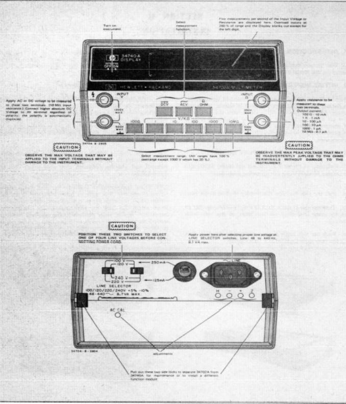
Figure 3-1. Front and Rear Panel Features.
3-0

Model 34702A |
TM 11-6625-2809-14 & P |
SECTION III
OPERATING INSTRUCTIONS
3-1. INTRODUCTION.
3-2. This section contains instructions and information which will assist you in proper operation of the Model 34702A Multimeter Module. A Model 34740A or 34750A Display Module is required to operate the Model 34702A. Included in this section is identification of controls, indicators and connectors; operating procedures; and BCD output code information (for use in conjunction with the 34721B BCD Module).
3-3. PANEL FEATURES.
3-4. The panel features of the instrument are described in Figure 3-1.
terminals without damaging the instrument. No more than 500 V should be applied between LO and Chassis (Grnd. ). Do not apply voltage between LO and Chassis when using the 34721A or 34721B BCD Module. These modules connect LO to Chassis when attached to the Model 34702A.
3-7. DC Voltage Measurement.
3-8. Set the Function switch to DCV, select the required voltage range, and apply the voltage to be measured to the INPUT V terminals.
3-9. AC Voltage Measurement.
3-5. FRONT PANEL OPERATION. |
3-10. Set the |
function |
switch to |
ACV, select |
the |
required voltage |
range, |
and apply |
the voltage to |
be |
|
|
measured to the INPUT V terminals. |
|
|
||
3-6. There are two manual controls; the function switch and the range switch (See Figure 3-1). Each range, except the 1000V range, has 100% overranging capability; e.g. using a four digit display module 1.9999 V can be measured on the I V range. The display blanks at 200% of range, indicating an overload.
Overload protection circuits allow up to 1200 V peak to be applied to the INPUT V terminals without damaging the instrument. Up to 350 V can be applied to the INPUT Ω.
3-11. Resistance Measurement.
3-12. Set the function switch to Ω (92), select the required resistance range, and connect the device to be measured to the INPUT Ω terminals.
3-13. 34721B/5055A OUTPUT CODES.
3-14. Output codes obtained from a 34721B BCD Module when used in conjunction with the Model 34702A and a display module are listed in Table 3-1. Refer to the 34721B Operating and Service Manual for further information regarding the BCD Module
.
|
|
Table 3-1. 34721B5055A Output Codes |
|
||||
|
|
|
|
|
|
|
|
Number |
Polarity |
|
|
|
|
|
|
Overload |
Range |
|
Function |
Overrange |
Digits Columns |
||
Printed |
Column 9 |
Column 8 |
Column 7 |
Column 6 |
1 through 5 |
||
|
|
k Ω |
|
Volts |
|
|
|
0 |
|
|
|
|
DCV |
underrange |
O |
1 |
+ |
10000 |
|
|
ACV |
overrange |
1 |
2 |
|
1000 |
|
1000 |
k Ω |
|
2 |
3 |
|
100 |
|
100 |
|
|
3 |
4 |
|
10 |
|
10 |
|
|
4 |
5 |
|
1 |
|
1 |
|
|
5 |
6 |
|
.1 |
|
.1 |
|
|
6 |
7 |
|
|
|
|
|
|
7 |
8 |
|
|
|
|
|
|
8 |
9 |
|
|
|
|
|
|
9 |
3-1
Model 34702A |
TM 11-6625-2809-14 & P |
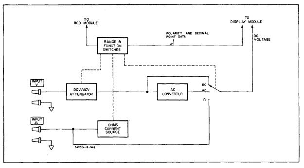
Figure 4-1. Block Diagram.
4-0
Model 34702A |
TM 11-6625-2809-14 & P |
SECTION IV
THEORY OF OPERATION
4-1. INTRODUCTION. |
4-9-. Range/Function Switches |
4-2. This section contains a description of the Model 34702 Multimeter in simplified form followed by a more detailed functional description. A detailed circuit schematic is shown in Figure 7-3.
4-3. BLOCK DIAGRAM DESCRIPTION.
4-4. The circuits of the Model 34702A can be divided into four major blocks shown in Figure 4-1.
4-5. ACV And DCV Attenuator.
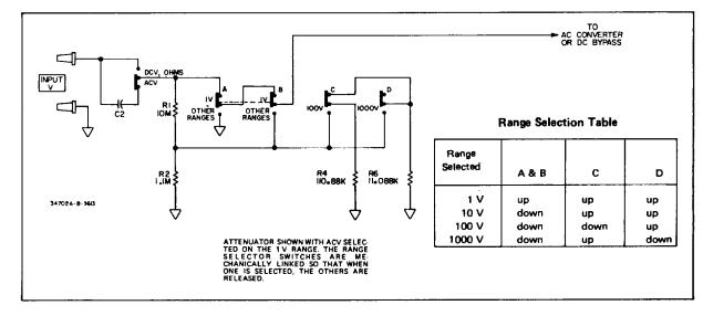
4-6. The ACV/DCV Attenuator reduces the level of the signal applied to the input so that it can be measured by the 34740A or 34750A Display Module. The signal can be attenuated by a factor of I, 10, 100 or 1000.
4-7. Current Source.
4-8. Resistance measurements are made by passing a known current through the resistor being measured and then measuring the voltage developed across the resistor. The current source supplies five different currents used by the six available ohmmeter ranges. Resistance of an unknown is measured by connecting it across the Ω terminals and selecting Ω function.
4-10. Range and Function switching is accomplished by manual selection. Data from the Range and Function switches is supplied to the Display Module, and to the BCD Module when it is connected.
4-11. AC Converter.
4-12. The AC Converter accepts ac voltage from the attenuator and changes it to a dc voltage proportional to the level of the applied signal.
4-13. DETAILED THEORY OF OPERATION.
4-14 ACV/DCV Attenuator.
4-15. Figure 4-2 shows the ACV/DCV Attenuator with its AC and DC voltage accuracy adjustments deleted. Resistors R3, R5, and R7, shown in Figure 7.3 are dc adjustments. Capacitors C3 through Cl 1, also shown in Figure 7-j provide ac compensation for the attenuator.
4-16. Ω Converter.
4-17. Current Source. A simplified diagram of the Ωmeter current source is shown in Figure 4-3a. Zener diode CRI6 is the voltage reference for the current source.
Figure 4-2. ACV/DCV Attenuator.
4-1

Model 34702A
Amplifier A is connected in a non-inverting configuration and Rb is adjusted such that 1 V (.1 V for the 10MIO range) is developed across Ra and Rb. Amplifier B has its + input connected to a stable dc voltage of -6.2 V. The - input is connected to the output of Amplifier A through the range reference resistors R52 - R56. The I V across Ra and Rb causes the output of Amplifier B to become more positive. This allows the current through Qx to vary such that the - input of Amplifier B becomes approximately -6.2 V. The input current to Amplifier B is very small. Consequently the current that flows through the range reference resistors is the same as the current supplied by the source of Qx. The drain current of Qx is almost identical to its source current because the gate current is extremely small. The drain current flows through Rx and develops a dc voltage which is applied to
TM 11-6625-2809-14 & P
the Display Module input. The output current, Ix, is changed for different resistance ranges by changing the value of Ra. On the 10 M Ω range
Switch Sb is in the 10 M Ω position which reduces the voltage between points 4 and 5 to .1 V.
4-18. Ohms Protection Circuit. The actual circuit represented by Qx in Figure 4-3a is shown in Figure 4- 3b. The ohmmeter circuits are protected for voltages applied to the "Ω (f’)" input up to 350 V peak. Large negative voltages are blocked by CR12. Large positive voltages are blocked by the high collector to base breakdown voltages of Q13 and Q14. CR13 conducts for positive voltages greater than approximately 2 V, causing CR14 to conduct.
Figure 4-3. Ohms Converter.
4-2
Model 34702A
turning on Q12. This places - 12 V at the collector of Q12 which turns off transistors QI 1, Q13, and Q14.
419.AC Measuring Circuits.
420.A simplified diagram of the circuits used to measure ac voltage is shown in Figure 4-4.
The attenuation of the input signal by the Attenuator for the four ac voltage ranges is:
Range |
Attenuation Factor |
1V |
X 1 |
1OV |
X 0.1 |
100V |
X 0.01 |
1000V |
X 0.001 |
TM 11-6625-2809-14 & P
The output voltage of the attenuator is buffered by the Impedance Converter. The voltage gain of the Impedance Converter is adjustable and is approximately one. Its input impedance is very high to minimize loading of the Attenuator and its output resistance is low to drive the Converter Amplifier. The AC Converter yields a dc output voltage that is proportional to the average value of the negative half-wave rectified input signal. The resulting voltage is filtered and measured by the Display Module.
4-21. Impedance Converter. A simplified diagram of the Impedance Converter is shown in Figure 4-5. The input transistor Q1 is a source follower. Transistors Q2 and Q3 constitute an amplifier that provides bias current to Q1 and a high input resistance (load resistance) for Q1. A positive going voltage at point 1 causes the voltage at point 2 to increase. This increased voltage at point 2 increases the
Figure 4-4. Ac/DC Converter.
4-3
Model 34702A
current through Q2. The increased current causes the voltage at point 4 to increase. Since Q3 is an emitter follower, point 3 will also increase and follow very closely the voltage at point 2. Since the output voltage is taken at the emitter of Q3, RI3 may be increased to make the gain of the amplifier greater than unity.
4-22. AC Converter. Refer to Figure 4-4 for the following discussion. Overall ac feedback is supplied from point 5 back to the inverting input. The voltage at point 5 is similar in shape to the voltage at point 2, inverted and about one-half the amplitude. Current for the negative half of the waveform at point 5 flows through CR8, R31 and R33. Current for the positive half of this waveform flows through CR9, R32 and R33. The output voltage is taken at the cathode of CR9, filtered by the Low Pass Filter and measured by the Display Module. The DC Feedback Amplifier provides a low frequency feedback path around the Converter Amplifier to keep the Converter Amplifier biased properly.
4-4
TM 11-6625-2809-14 & P
Figure 4-5. Impedance Converter.

TM 11-6625-2809-14 & P

 WARNING


These servicing instructions are for use by qualified personnel only. To avoid electrical shock, do not perform any servicing other than that contained in the operating instructions unless you are qualified to do so.
5-0

Model 34702A |
TM 11-6625-2809-14 & P |
SECTION V.
MAINTENANCE
5-1. INTRODUCTION.
5-2. This section contains information necessary for maintenance of the -hp- Model 34702A Multimeter. Included are Performance Tests and Adjustment Procedures for the 30 day, 90 day, 6 month, and I year intervals referred to in Table 1-1. To determine the optimum calibration interval for your instrument, refer to MIL Specification MILC-45662A. If, after completing the Performance Checks, you find that the instrument does not meet its required specifications, refer to the Adjustment Procedure (Paragraph 5-16). Attempt to readjust the instrument to bring it into specification. If, after adjusting the instrument, it is still out of specification, refer to troubleshooting in Section VII.
Table 5-1. Recommended Test Equipment.
Instrument |
Required |
Recommended |
Type |
Characteristics |
Model |
AC Calibrator |
1 V, 10 V, 100 V |
-hp- Model |
|
1000 V, 45 Hz to |
745A/746A |
|
100 kHz |
|
|
Accuracy: +0.04% |
|
|
of setting (45 Hz to |
|
|
20 kHz) |
|
|
+ 0.15% of setting |
|
|
(100 kHz) |
|
100 Ω, 1ΚΩ |
Accuracy: +0.01% |
General Radio |
10ΚΩ, 100ΚΩ |
|
Model GR 1433-Z |
1ΜΩ, 10ΜΩ |
|
Decade Resistor |
|
|
|
standard resistors |
|
|
5-3. RECOMMENDED TEST EQUIPMENT.
5-4. The test equipment that is recommended for maintaining the Model 34702A is listed in Table 5-1. If the recommended model is not available, use equipment that has specifications equal to or better than those listed.
5-5. PERFORMANCE TESTS.
5-6. The following tests verify that the Model 34702A is operating properly and meets the specifications listed in Table 1-1 of this manual. These tests should be completed before any attempt is made to adjust the instrument.
5-7. A Performance Test Record is provided at the end of this section for recording the results of the Performance Tests.
5-8. All of the following tests have been written to include the use of either a 34740A or 34750A Display Module.
5-9. DC Accuracy Test (DCV Function).
DESCRIPTION:
This test verifies the ability of the Model 34702A to measure dc voltage accurately within the specification limits.
SPECIFICATION.
34740A
Accuracy (+ 23o C + 5o C), < 95% RH):
30 days |
+ (0.03% of reading + .01% of range) |
90 days |
+ (0.04% of reading + .01% of range) |
6 mo. |
+ (0.05% of reading + .02% of range) |
1 yr |
.+ (0.06% of reading + .02% of range) |
DC Standard |
1 V, 10 V, 100 V, |
-hp- 740B |
|
1000 V Ranges |
|
|
Accuracy: +0.008% |
|
Electronic |
Capable of measur- |
-hp- Model 5300A/ |
Counter |
ing the period of |
5302A |
|
50 Hz or 60 Hz to |
|
|
within + .01% |
|
34750A
Accuracy (+ 23oC + 5oC), <95% RH):
30 days |
+(0.025% of reading + .005% of range) |
90 days |
±(0.035% of reading + .005% of range) |
6 mo. |
±(0.045% of reading + .007% of range) |
1 yr. |
±(0.06% of reading + .01% of range) |
RECOMMENDED TEST EQUIPMENT:
DC Standard, -hp- Model 740B
TEST PROCEDURE:
a.Select the DCV function of the Model 34702A and connect a dc standard (-hp- Model 740B or equivalent) to the 34702A INPUT V terminals.
b.Check dc accuracy for both polarities of input according to Table 5-2. Apply short to 34702A input to check 0 V reading on all ranges.
NOTE
With 1000 V applied only the positive polarity is checked due to the possibility of arcing within the Model 740B.
Rev. B 5-1
Model 34702A |
PERFORMANCE TEST |
TM 11-6625-2809-14 & P |
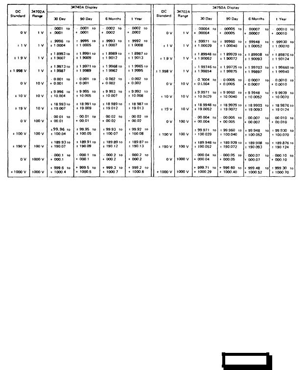
Table 5-2. DC Accuracy.
5-10. Input Impedance Test (DCV and ACV
Function).
DESCRIPTION:
Input impedance affects the ability of a voltmeter to accurately measure a given voltage because of loading effects caused by the impedance Normally, it is desirable to achieve as high an input impedance as possible. This check ensures that the input Impedance of the Model 34702A meets the specifications listed below.
SPECIFIC ATION: |
|
Input Resistance |
|
1 and 10 V ranges: |
11.11 ΜΩ + 0.2% <80 pF |
100 V range: |
10.1 ΜΩ + 0.2% <80 pF |
1000 V range: |
10 ΜΩ ± 0.2% < 80 pF |
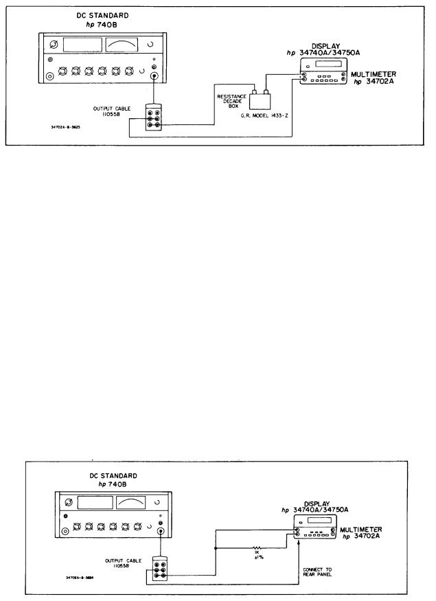
RECOMMENDED TEST EQUIPMENT:
b.Set the resistance decade to 10 ΜΩ and then shunt it with a jumper lead. Set the DC standard for + 1.0000 V (34740A Display) or + 1.00000 V (34750A Display) as observed on the Display Module.
c.Remove the jumper lead and again observe the display. It should read between .5258V and .5268V (34740A) or between .52582 and .52681 (34750A).
NOTE
The 34702A is not checked on the 10 V range since the input circuit is equivalent for both the 1 V and the 10 V ranges.
d.Set the Model 34702A to the 100 V range and short the resistance box with a jumper lead.
e.Set the dc standard for + 100.00 V (34740A) or
+100.000 V (34750A) as observed on the Display Module.
AC Calibrator, -hp- Model 745A
DC Standard, -hp- Model 740B
Resistance Decade, GR Model 1433-Z
TEST PROCEDURE:
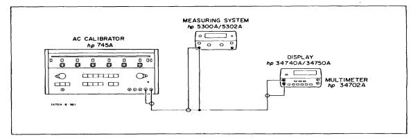
a. Connect the equipment as shown ill Figure 5-1. The Model 34702A should be set to DCV on the 1 V range.
Rev. B 5-2
WARNING
Use extreme caution when removing or replacing the jumper in Steps f, g and i to avoid electrical shock when performing the input impedance test on the 100 V’ and 1000 V ranges.
TM 11-6625-2809-14 & P
Model 34702A |
PERFORMANCE TEST |
Figure 5-1. Input Impedence Test.
f.Turn the dc standard OUTPUT to OFF. Remove the jumper from the resistance box. Set dc standard OUTPUT to ON and again observe the display. It should read 50.20 to 50.30 (34740A) or 50.201 to 50.301 (34750A).
g.Turn the dc standard OUTPUT to OFF. Set the Model 34702A to the 1000 V range and short the resistance box with a jumper lead.
h.Turn the dc standard OUTPUT to ON. Set
the dc standard for + 1000.0 V (34740A) or + 1000.00 V (34750A) as observed on the Display Module.
i. Turn the dc standard OUTPUT to OFF. Remove the jumper from the resistance box. Turn the dc standard OUTPUT to ON and again observe the display. It should read 499.7 to 500.7 (34740A) or 499.75 to 500.75 (34750A).
j. Set the dc standard OUTPUT to zero. Replace dc standard with the ac standard.
k. Set the Model 34702A to the 1 V range. Replace the resistance box with a 100 κΩ resistor (-hp- Part Number 0757-0465). Connect one end of the resistor directly to the HI terminal. Set the ac standard frequency to I kHz. Adjust the ac standard amplitude for + 1.0000 V i 1 count(34740A) or + 1.00000 V + 1 count (34750A) as observed on the Display Module.
I. Change the ac standard frequency to 20 kHz. The 34702A display should indicate >.7059 (34740A) or>
.70594 (34750A). This verifies the 34702A input capacity specification.
5-1. DC Effective Common Mode Rejection.
DESCRIPTION:
Effective Common Mode Rejection (ECMR) is a measure of the effect of a common mode source on the measured value or readout of the instrument with a 1kohm unbalance. Typically ECMR is measured in decibels (dB) and can be calculated by the following formula:
Common Mode Voltage Applied
ECMR (dB) = 20 log10 (________________________________________)
Change in Display Indication
SPECIFICATION
:
Effective Common Mode Rejection (I κΩ unbalance): > 80 dB.
RECOMMENDED TEST EQUIPMENT: DC Standard, -hp- Model 740B
Resistor, I κΩ t 1% (resistance decade may be used for this)
Figure 5-2. Effective Common Mode Rejection
Rev. C 5-3
Model 34702A |
PERFORMANCE TEST |
TM 11-6625-2809-14 & P |
TEST PROCEDURE
a.Disconnect all previous connections to the Model 34702A input and connect the equipment as shown in Figure 5-2. Set the dc standard for a +10 V output. Set the 34702A to the I V range.
b.Observe the voltmeter display. It should read less than 10 counts (34740A Display) or 100 counts (34750A Display). This verifies an effective common mode rejection at dc of > 80 dB.
5-12. Normal Mode Rejection.
DESCRIPTION:
Normal Mode Rejection (NMR) is a measure of the ability of the Model 34702A to reject ac signals applied to the INPUT V terminals while the instrument is operating in DCV function. NMR is measured in decibels (dB) and can be calculated by the following formula:
Peak Normal Mode Voltage
NMR (dB) = 20 log10(____________________________________)
Peak Display Indication
SPECIFICATION:
Normal Mode Rejection: Greater than 60 dB (at 50 Hz t 0.1%or 60 Hz ± 0.1%).
RECOMMENDED TEST EQUIPMENT:
AC Calibrator, -hp- Model 745A
Electronic Counter, -hp- Model 5300A/5302A
TEST PROCEDURE:
a.Disconnect all previous connections to the 34702A input and connect the equipment as shown in Figure 5-3. Set the Model 34702A to DCV and the 1 V range.
b.Adjust the ac calibrator output for .707 V rms (1V
peak).
c. Set the counter controls to measure period and adjust the ac calibrator frequency for a counter indication between 16.650 ms and 16.683 ms (19.980 ms to 20.020 ms for Option 050). The Display Module should read <10 counts (34740A Display) or <100 counts (34750A Display).
5-13. AC Accuracy.
DESCRIPTION:
This test verifies the ability of the Model 34702A to measure ac voltage accurately to within the specification tolerances.
SPECIFICATION:
34740A
Accuracy (+ 23°C ± 5°C, <95% RH)'
30 days |
|
45 Hz to 20 kHz |
+(0.25% of reading + |
|
.05% of range) |
20 kHz to 100 kHz |
+(0.75% of reading + |
|
.05% of range) |
90 days |
|
45 Hz to 20 kHz |
+(0.30°c of reading + |
|
.05% of range) |
20 kHz to 100 kHz |
+(0.80% of reading + |
|
.05% of range) |
6 mo. |
|
45 Hz to 20 kHz |
+(0.35% of reading + |
|
.05% of range) |
20 kHz to 100 kHz |
+(0.85% of reading + |
|
.05% of range) |
I yr. |
|
45 Hz to 20 kHz |
+(0.50% of reading + |
|
0.05% of range) |
20 kHz to 100 kHz |
+(1.0% of reading + |
|
0.05% of range) |
Figure 5-3. Normal Mode Rejection.
Rev. A 5-4

Model 34702A |
PERFORMANCE TEST |
TM 11-6625-2809-14 & P |
34750A
Accuracy (+ 23oC + 5°C, < 95% RH):
30 days |
|
45 Hz to 20 kHz |
+(0.25% of reading + |
|
.05% of range) |
20 kHz to 100 kHz |
+(.75% of reading + |
|
.05% of range) |
90 days |
|
45 Hz to 20 kHz |
±(.3% of reading + |
|
.05% of range) |
20 kHz to 100 kHz |
+(.8% of reading + |
|
.05% of range) |
6 mo. |
|
45 Hz to 20 kHz |
+(.35% of reading + |
|
.05% of range) |
20 kHz to 100 kHz |
+(.85% of reading + |
|
.05% of range) |
1 yr. |
|
45 Hz to 20 kHz |
±(0.50% of reading + |
|
0.05% of range) |
20 kHz to 100 kHz |
±(1.0% of reading + |
|
0.05% of range) |
RECOMMENDED TEST EQUIPMENT:
AC Calibrator/High Voltage Amplifier, -hp- Model 745A/746A or equivalent.
TEST PROCEDURE:
a.Set the Model 34702A function switch to ACV and select the I V range. Apply short to 34702A input and check 0 V reading on all ranges.
b.Using an ac calibrator and a high voltage amplifier (-hp- Model 745A/746A recommended), check the accuracy of the Model 34702A for inputs other than 0 V at 45 Hz and 20 kHz using Table 5-3(a). Also check the accuracy for these inputs at 100 kHz using Table 5- 3(b). All readings should be within the limits specified by the tables.
514.Response Time.
DESCRIPTION:
This test verifies the ability of the Model 34702A to respond quickly to changes in input voltage.
SPECIFICATION:
34740A
Response time: < 2 s to within + 0.3% of final value or 20 counts, whichever is greater.
Table 5-3. (a). AC Accuracy (45Hz and 20 kHz).
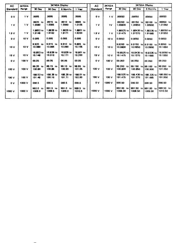
Rev. B 5-5
Model 34702A |
PERFORMANCE TEST |
TM 11-6625-2809-14 & P |
Table 5-3(b). AC Accuracy (100 kHz).
34750A
Response time: <2 s to within t 0.3% of final value or 200 counts, whichever is greater.
RECOMMENDED TEST EQUIPMENT:
AC Calibrator, -hp- Model 745A or equivalent
TEST PROCEDURE:
a.Set the ac calibrator output to 10 V at I kHz. Set the 34702A to ACV on the 10 V range.
b.Connect the output of the ac calibrator to the 34702A INPUT V terminals while observing the 34740A/34750A Display Module. The display indication should read within 30 counts (34740A) or 300 counts (34750A) of its final value within two seconds after the 34702A is connected to the ac calibrator.
5-15. Ohms Accuracy.
DESCRIPTION:
This test verifies the ability of the Model 34702A to accurately measure resistance to within the limits of the specification given below.
SPECIFICATION:
34740A
Accuracy (+ 23oC + 5°C, < 95% RH):
30 days |
|
10 ΜΩ range |
+(0.25% of reading + |
|
0.02% of range) |
All other |
+(0.05% of reading + |
ranges |
0.02% of range) |
90 days |
|
10 ΜΩ range |
+(0.30% of reading + |
|
0.02% of range) |
All other |
+(0.06% of reading + |
ranges |
0.02% of range) |
6 mo. |
|
10 ΜΩ range |
+(0.35% of reading + |
|
0.03% of range) |
All other |
±(0.07% of reading + |
ranges |
0.03% of range) |
1 yr. |
|
10 ΜΩ range |
+(0.50% of reading + |
|
0.03% of range) |
All other |
+(0.1 1% of reading + |
ranges |
0.03% of range) |
34750A
Accuracy (+ 23oC + 5°C, <95% RH):
30 days |
|
10 ΜΩ range |
+(0.25% of reading + |
|
0.015% of range) |
All other |
+(0.045% of reading + |
ranges |
0.015% of range) |
Rev. A 5-6

Model 34702A |
PERFORMANCE TEST |
TM 11-6625-2809-14 & P |
90 days |
|
10 ΜΩ range |
+(0.3% of reading + |
|
0.015% of range) |
All other |
±(0.055% of reading + |
ranges |
0.015% of range) |
6 mo. |
|
10 ΜΩ range |
+(0.35% of reading + |
|
0.02% of range) |
All other |
+(0.065% of reading + |
ranges |
0.02% of range) |
1 yr. |
|
10 ΜΩ range |
±(0.50% of reading + |
|
0.02% of range) |
All other |
+(0.1 1% of reading + |
ranges |
0.02% of range) |
RECOMMENDED TEST EQUIPMENT:
Resistance Decade, GR Model 1433-Z or equivalent.
NOTE
Due to temperature change inside the instrument between line and battery operation, the voltage references in the Display Module must be adjusted when changing modes to achieve these specifications.
TEST PROCEDURE:
a.Connect a resistance decade with 100 f through ΜΩ steps to the INPUT i2 terminals of the Model 34702A.
b.Refer to Table 5-4 and check the accuracy of the 34702A on the 100 Ω through 10 ΜΩ ranges.
Table 5-4. Ohms Accuracy Test.
5-7
Loading...