


 Loading...
YM2608
OPNA
Application Manual
Transcribed by Nemesis
OCR by Adobe Acrobat 8 Professional
Automated translation using http://www.excite.co.jp/world/english Additional translation using http://translate.google.com
Kanji reference provided by http://nihongo.j-talk.com/parser/search 30/6/2008
Yamaha Motor Co., Ltd.
1
Outline
YAMAHA sound source LSI OPNA is a compound type sound source system that enhances the function in addition while having interchangeability named OPN(YM2203). The digital rhythm sound source with a high sampling function and reality demanded from the new generation sound source in addition to six FM sound sound pronunciation simultaneously was built into. In addition, it risked it for two channel output.
FM sound source, SSG sound source, ADPCM sound source, and the system configuration by 4 sound source part of the rhythm sound source flexibly correspond to all the sound concepts.
Feature
• |
FM Sound Source |
Four operators six-sound pronunciation simultaneously. |
|
|
|
With built-in |
sine wave LFO function |
|
|
YM2203 and software compatibility full. |
|
• |
SSG Sound Source |
YM2203 and software compatibility full. |
|
|
|
(After mixing, the output outputs 3ch.) |
|
• |
ADPCM Sound Source |
ADPCM voice analysis and synthetic function. |
|
|
|
Accessible of |
memory that external memory and CPU |
|
|
manage. |
|
|
|
Sampling rate |
16KHz max. |
• |
Rhythm Sound Source |
Six digital rhythm tones. (pronunciation control by |
|
|
|
event method) |
|
• |
DAC output |
Exclusive use |
DAC YM3016. 2ch output. |
• |
Master clock |
8MHz |
|
•Nch-Si gate MOS LSI
•5V single power supply
•64pin plastic SDIP
2
Chapter 1 Composition and Function
1-1: Prime function
The basic function of OPNA can be divided roughly into four sound source part of FM sound source, SSG sound source, and ADPCM sound source and the rhythm sound source.
1) FM sound source part
The basic function of the FM sound source part is the same as OPN(YM2203). (It is a function that the part is enhanced.)
Pronunciation mode |
Four operator FM method and six sound pronunciation |
|
simultaneously. |
Algorithm |
Eight kinds. |
Parameter |
The register address and refer to the FM sound source |
|
part. |
LFO function |
Sine wave LFO. Pitch (PM) and, it modulates amplitude |
|
(AM). |
|
The LFO frequency is changeable. AM on/off is possible |
|
of PMS, the AMS control, and each operator. |
Compound sine wave synthesis |
One sound is possible in six sounds. |
Timer function |
Two kinds of timers of A and B. |
Output control |
On/off of L and R. |
2) SSG sound source part
The SSG sound source part is the same as OPN excluding the output method.
Pronunciation form |
Three rectangular liquid sounds |
+ white noise. |
|
Function of each data |
Refer to the register address. |
|
|
Output |
It outputs it from one terminal |
by |
internal mixing. |
I/O port |
Eight bit general purpose I/O port |
x2 |
|
3) Rhythm sound source part
The rhythm sound source part is a digital rhythm by ADPCM voice synthesis method to build rhythm ROM into.
Pronunciation tone |
6 sounds (bass drum, snare, rim shot, Tamm, cymbals, |
|
|
and high hat cymbals) |
|
Pronunciation control |
Event method (It is possible to dump it) |
|
Level control |
Each tone |
independence can control. |
|
The total |
level can control. |
Output control |
On/off of |
L and R. |
3
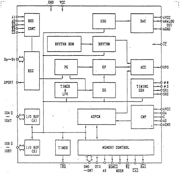
4) ADPCM sound source part
Speech analysis, synthesis, and external memory control of ADPCM sound source part. It is composed of the AD/DA conversion function.
Sampling rate |
2kHz-16kHz |
AD/DA conversion |
8bit |
ADPCM analysis |
4bit |
Linear interpolation rate |
55.5kHz |
Data memory |
Memory that external RAM ROM or CPU manages. |
External memory capacity |
256kbytes (max) |
|
DRAM access x1bit, x8bit it is possible to select |
Output control |
On/off of L and R. |
No sound discrimination |
The state under the analysis of a no sound can be |
|
identified. |
5) DAC |
|
Exclusive use DAC YM3016 is used. |
|
1-2: Block diagram |
|
4

1-3: Terminal arrangement chart
Note: This figure is TOP VIEW.
* It is a pull-up in Vcc. the terminal of the sign
5
1-4: Terminal function |
|
|
• |
φM |
Master clock (standard 8MHz) of OPNA is input. |
• |
φS,SH1,SH2 |
It is clock (φS) for DAC and signal (SH1, SH2) of the cycle. |
• |
OPO |
It is a serial data of FM, ADPCM, and rhythm each sound |
|
|
source part output. |
• |
DO-D7 |
It is passing of interactive data of 8bit. CPU and data are |
|
|
exchanged. |
• |
!CS,!RD,!WR,A1,A0 |
Data passing (D0-D7) is controlled. |
• |
!IRQ |
The interrupt signal is output. It is an open drain output. |
• |
ANALOG OUT |
It is an analog output terminal in the SSG sound source part. |
|
|
It is source for an output. |
•10A0-10A7,
|
10B0-10B7 |
It is 8bit general purpose I/O port of two affiliates. It is |
|
|
|
a pull-up in Vcc. |
|
• |
DM0-DM7 |
Each signal of address (AO-A7), data input (D10-D17), and |
|
|
|
data output (D01-D07) of an external memory is done to each |
|
|
|
terminal of corresponding DM0-DM7 in the multiplex. |
|
• |
A8,DT0 |
A8 connects DTO with data output (D00) in address (A8) of an |
|
|
|
external memory. |
|
• |
!RAS,!CAS,!WE |
It is a |
control signal of an external memory. |
|
|
When an |
external memory is DRAM, it is connected with the |
|
|
corresponding each terminal. |
|
|
|
It uses |
it for latch signal (!RAS !CAS) of the address for |
|
|
ROM. !RAS : to RAS address. !CAS corresponds to the CAS |
|
|
|
address. |
|
• |
MDEN,!ROMCS |
It is a |
timing signal that takes the data of an external |
|
|
memory. |
|
|
|
When MDEN is“1”, DRAM data is put on DM1-DM7 and DTO. |
|
|
|
When !ROMCS is“0”, ROM data is put on DM1-DM7 and DTO. |
|
• |
AD,C,DA |
It is a |
terminal for the AD conversion. |
|
|
AD is an analog input terminal, and the input voltage of |
|
|
|
convertible AD is a range of Vce/2 Vce/4(v). |
|
|
|
The terminal DA is connected with the DAC output with the |
|
|
|
terminal that inputs a standard voltage when AD is converted. |
|
• |
SPOFF |
It is necessary to separate the amplifier and the |
|
|
|
speaker |
to use DA Comparta as a reference voltage generator |
|
|
when AD |
is converted. This terminal is used as a control |
|
|
terminal for that. |
|
• |
!IC |
The operation of OPNA is initialized. |
|
• |
!TEST |
It is a |
terminal for the test of LSI. |
• |
GND,AGND |
It is a |
ground terminal. |
• |
Vcc,AVcc |
It is a |
power supply terminal of +5V. |
6

1-5: Data bus control
The data bus control of read/write etc. of addressing and data is done with !CS !WR !RD A1 AO. Figure 1-* and Table 1-1 show the allocation of the register address at this time and the control mode of the register.
|
|
|
|
|
|
|
|
|
A1=“0” |
|
|
A1=“1” |
|
|
|
|
|
|
|
|
|
|
|
|
|
||
|
|
$00-$0F |
|
SSG |
|
$00-$10 |
ADPCM |
|
|||||
|
|
|
|
|
|
|
|
|
|
|
|
||
|
|
$10-$1F |
|
Rhythm |
|
|
|
|
|||||
|
|
|
|
|
|
|
|
|
|
|
|
||
|
|
$20-$2F |
|
Commonness part |
|
|
|
|
|||||
|
|
|
|
|
|
|
of FM |
|
|
|
|
||
|
|
$30- |
|
|
|
|
|
|
|
$30- |
|
|
|
|
|
|
|
|
FM |
|
|
|
FM |
|
|||
|
|
|
|
|
|
|
|
|
|
|
|
||
|
|
|
|
$B6 |
|
(CH1-CH3) |
|
$B6 |
(CH4-CH6) |
|
|||
|
|
|
|
|
|
|
|
|
|
|
|||
|
|
|
|
|
|
|
|
|
|
|
|
|
Figure 1-* |
|
|
|
|
|
|
|
|
|
|
|
|
|
|
|
|
|
|
|
|
|
|
Table 1-1: Content of data passing control |
|||||
|
|
|
|
|
|
|
|
|
|
|
|
|
|
!CS |
!RD |
|
!WR |
|
A1 |
|
A0 |
|
Range of |
|
|
Content |
|
|
|
|
|
|
|
|
|
|
address |
|
|
|
|
0 |
1 |
|
0 |
|
0 |
|
0 |
|
00-2F |
Addressing of SSG, commonness part of FM, and rhythm |
|||
|
|
|
|
|
|
|
|
|
|||||
|
|
|
|
30-B6 |
Addressing of FM channel 1-3 |
||||||||
|
|
|
|
|
|
|
|
|
|||||
|
|
|
|
|
|
|
|
|
|
|
|||
0 |
1 |
|
0 |
|
0 |
|
1 |
|
00-2F |
Data write of SSG, commonness part of FM, and rhythm |
|||
|
|
|
|
|
|
|
|
|
|||||
|
|
|
|
30-B6 |
Data write of FM channel 1-3 |
||||||||
|
|
|
|
|
|
|
|
|
|||||
|
|
|
|
|
|
|
|
|
|
|
|||
0 |
1 |
|
0 |
|
1 |
|
0 |
|
00-10 |
Addressing related to ADPCM |
|||
|
|
|
|
|
|
|
|
|
|||||
|
|
|
|
30-B6 |
Addressing of FM channel 4-6 |
||||||||
|
|
|
|
|
|
|
|
|
|||||
|
|
|
|
|
|
|
|
|
|
|
|||
0 |
1 |
|
0 |
|
1 |
|
1 |
|
00-10 |
Data write related to ADPCM |
|||
|
|
|
|
|
|
|
|
|
|||||
|
|
|
|
30-B6 |
Data write of FM channel 4-6 |
||||||||
|
|
|
|
|
|
|
|
|
|||||
|
|
|
|
|
|
|
|
|
|
|
|||
0 |
0 |
|
1 |
|
0 |
|
0 |
|
XX |
Data read of status O |
|||
|
|
|
|
|
|
|
|
|
|
|
|||
0 |
0 |
|
1 |
|
0 |
|
1 |
|
00-0F |
Read of data of SSG register |
|||
|
|
|
|
|
|
|
|
|
|||||
|
|
|
|
FF |
Device identification code read |
||||||||
|
|
|
|
|
|
|
|
|
|||||
|
|
|
|
|
|
|
|
|
|
|
|||
0 |
0 |
|
1 |
|
1 |
|
0 |
|
XX |
Data read of status 1 |
|||
|
|
|
|
|
|
|
|
|
|
|
|||
0 |
0 |
|
1 |
|
1 |
|
1 |
|
08,0F |
Read of ADPCM and PCM data |
|||
|
|
|
|
|
|
|
|
|
|
|
|
|
|
1 |
X |
|
X |
|
X |
|
X |
|
XX |
Inactive mode |
|
|
|
|
|
|
|
|
|
|
|
|
|
|
|
|
|
7
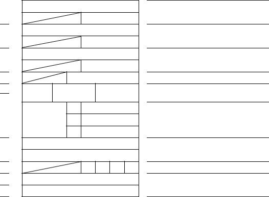
(a) READ/WRITE DATA (part SSG) |
|
|
||||||
Address |
D7 |
D6 |
D5 |
D4 |
D3 |
D2 |
D1 |
D0 |
00 |
|
|
|
Fine Tune |
|
|
|
|
01 |
|
|
|
|
|
Coarse Tune |
|
|
02 |
|
|
|
Fine Tune |
|
|
|
|
03 |
|
|
|
|
|
Coarse Tune |
|
|
04 |
|
|
|
Fine Tune |
|
|
|
|
05 |
|
|
|
|
|
Coarse Tune |
|
|
06 |
|
|
|
|
Period Control |
|
||
07 |
IN/OUT |
|
/Noise |
|
|
/Tone |
|
|
|
IOB |
IOA |
|
|
|
|
|
|
08 |
|
|
|
M |
|
Level |
|
|
09 |
|
|
|
M |
|
Level |
|
|
0A |
|
|
|
M |
|
Level |
|
|
0B |
|
|
|
Fine Tune |
|
|
|
|
0C |
|
|
|
Coarse Tune |
|
|
||
0D |
|
|
|
|
CON |
ATT |
ALT |
HLD |
0E |
|
|
|
I/O PortA |
|
|
|
|
0F |
|
|
|
I/O PortB |
|
|
|
|
Comment
Channel-A Tone Period
Channel-B Tone Period
Channel-C Tone Period
Noise Period
/ENABLE
Channel-A Amplitude
Channel-B Amplitide
Channel-C Amplitude
Envelop Period
Envelop Shape Cycle
I/O Port Data
8
(b) WRITE DATA (part RHYTHM)
Address |
D7 |
D6 |
D5 |
D4 |
D3 |
D2 |
D1 |
D0 |
|
Comment |
||
|
|
|
|
|
|
|
|
|
|
|
|
|
10 |
|
DM |
|
|
|
RKON |
|
|
|
Dump/rhythm KON |
||
|
|
|
|
|
|
|
|
|
|
|
|
|
11 |
|
|
|
|
|
RTL |
|
|
|
|
Rhythm Total Level |
|
|
|
|
|
|
|
|
|
|
|
|
|
|
12 |
|
|
|
|
TEST |
|
|
|
|
LSI TEST DATA |
||
|
|
|
|
|
|
|
|
|
|
|
|
|
18 |
- |
L |
R |
|
|
|
IL |
|
|
|
Output Select/Instrument Level |
|
|
|
1D |
|
|
|
|
|
|
||||
|
|
|
|
|
|
|
|
|
|
|
|
|
|
|
|
|
|
|
|
|
|
|
|
|
|
9
(c) WRITE DATA (FM part)
Address |
D7 |
D6 |
D5 |
D4 |
D3 |
D2 |
D1 |
D0 |
||
|
|
|
|
|
|
|
|
|
|
|
21 |
|
|
|
|
TEST |
|
|
|
||
|
|
|
|
|
|
|
|
|
|
|
22 |
|
|
|
|
|
|
|
LFO |
|
|
|
|
|
|
|
|
|
|
|
|
|
24TIMER-A
25 TIMER-A
26TIMER-B
27 |
|
MODE |
|
RESET |
|
ENABLE |
|
LOAD |
|
|||||
|
|
|
|
B |
|
A |
|
B |
A |
|
B |
A |
||
|
|
|
|
|
|
|
|
|||||||
|
|
|
|
|
|
|
|
|
|
|
|
|
|
|
28 |
|
|
|
SLOT |
|
|
|
|
|
|
|
CH |
|
|
|
|
|
|
|
|
|
|
|
|
|
|
|
||
29 |
|
SCH |
|
|
|
|
|
|
IRQ ENABLE |
|
||||
2D |
|
|
|
|
|
|
|
|
|
|
|
|
|
|
|
|
|
|
|
|
|
|
|
|
|
|
|
|
|
2E |
|
|
|
|
|
|
|
|
|
|
|
|
|
|
|
|
|
|
|
|
|
|
|
|
|
|
|
|
|
2F |
|
|
|
|
|
|
|
|
|
|
|
|
|
|
|
|
|
|
|
|
|
|
|
|
|
|
|
|
|
|
|
|
|
|
|
|
|
|
|
|
|
|
|
|
30 |
- |
|
|
|
DT |
|
|
|
|
|
MULTI |
|
||
|
3E |
|
|
|
|
|
|
|
|
|
||||
|
|
|
|
|
|
|
|
|
|
|
|
|
|
|
|
|
|
|
|
|
|
|
|
|
|
|
|
|
|
40 |
- |
|
|
|
|
|
|
|
TL |
|
|
|
|
|
|
4E |
|
|
|
|
|
|
|
|
|
|
|
||
|
|
|
|
|
|
|
|
|
|
|
|
|
|
|
|
|
|
|
|
|
|
|
|
|
|
|
|
|
|
50 |
- |
KS |
|
|
|
|
|
|
|
AR |
|
|
|
|
|
5E |
|
|
|
|
|
|
|
|
|
|
|||
|
|
|
|
|
|
|
|
|
|
|
|
|
|
|
|
|
|
|
|
|
|
|
|
|
|
|
|
|
|
60 |
- |
AMON |
|
|
|
|
|
|
|
|
DR |
|
|
|
|
6E |
|
|
|
|
|
|
|
|
|
|
|
||
|
|
|
|
|
|
|
|
|
|
|
|
|
|
|
70 |
- |
|
|
|
|
|
|
|
|
|
SR |
|
|
|
|
7E |
|
|
|
|
|
|
|
|
|
|
|
|
|
|
|
|
|
|
|
|
|
|
|
|
|
|
|
|
|
|
|
|
|
|
|
|
|
|
|
|
|
|
|
80 |
- |
|
|
SL |
|
|
|
|
|
|
RR |
|
||
|
8E |
|
|
|
|
|
|
|
|
|
||||
|
|
|
|
|
|
|
|
|
|
|
|
|
|
|
|
|
|
|
|
|
|
|
|
|
|
|
|
|
|
90 |
- |
|
|
|
|
|
|
|
|
|
SSG-EG |
|
||
|
9E |
|
|
|
|
|
|
|
|
|
|
|||
|
|
|
|
|
|
|
|
|
|
|
|
|
|
|
|
|
|
|
|
|
|
|
|
|
|
|
|
|
|
A0 |
|
|
|
|
|
|
|
|
|
|
|
|
|
|
A1 |
|
|
|
|
|
|
F-Num 1 |
|
|
|
|
|||
A2 |
|
|
|
|
|
|
|
|
|
|
|
|
|
|
|
|
|
|
|
|
|
|
|
|
|
|
|
|
|
A4 |
|
|
|
|
|
|
|
|
|
|
|
|
|
|
A5 |
|
|
|
|
|
|
BLOCK |
|
|
|
F-Num 2 |
|
||
A6 |
|
|
|
|
|
|
|
|
|
|
|
|
|
|
|
|
|
|
|
|
|
|
|
|
|
|
|
|
|
A8 |
|
|
|
|
|
|
|
|
|
|
|
|
|
|
A9 |
|
|
|
|
3 CH * F-Num 1 |
|
|
|
|
|||||
AA |
|
|
|
|
|
|
|
|
|
|
|
|
|
|
|
|
|
|
|
|
|
|
|
|
|
|
|
|
|
AC |
|
|
|
|
|
3 CH * |
|
|
|
3 CH * |
|
|||
AD |
|
|
|
|
|
|
|
|
|
|||||
|
|
|
|
|
|
BLOCK |
|
|
|
F-Num 2 |
|
|||
AE |
|
|
|
|
|
|
|
|
|
|
||||
|
|
|
|
|
|
|
|
|
|
|
|
|
|
|
|
|
|
|
|
|
|
|
|
|
|
|
|
|
|
B0 |
|
|
|
|
|
|
|
|
|
|
|
|
|
|
B1 |
|
|
|
|
|
|
FB |
|
|
|
CONNECT |
|
||
B2 |
|
|
|
|
|
|
|
|
|
|
|
|
|
|
|
|
|
|
|
|
|
|
|
|
|
|
|
|
|
B4 |
|
|
|
|
|
|
|
|
|
|
|
|
|
|
B5 |
|
L |
|
R |
|
AMS |
|
|
|
|
|
PMS |
|
|
B6 |
|
|
|
|
|
|
|
|
|
|
|
|
|
|
|
|
|
|
|
|
|
|
|
|
|
|
|
|
|
Comment
LSI TEST DATA
LFO FREQ CONTROL
TIMER-A upper 8 Bits
TIMER-A lower 2 Bits
TIMER-B DATA
TIMER-A/B Control and
3 CH Mode
Key-ON/OFF, CH is specified with DO,D1,D2
IRQ Enable, SCH
It is Set as for prescaler.
1/3, 1/6 Selection of dividing frequency
The machine of dividing frequency is set to 1/2.
Detune/Multiple
(33, 37, 3B There is no Address)
Total Level |
|
(43, 47, 4B There |
is no Address) |
|
|
Key Scale/Attack Rate |
|
(53, 57, 5B There |
is no Address) |
|
|
Decay Rate/AMON |
|
(63, 67, 6B There |
is no Address) |
|
|
Sustain Rate |
|
(73, 77, 7B There |
is no Address) |
|
|
Sustain Level/Release Rate |
|
(83, 87, 8B There |
is no Address) |
|
|
SSG-Type Envelope |
Control |
(93, 97, 9B There |
is no Address) |
|
|
F-Numbers/BLOCK
3 CH-3 slot F-Numbers/BLOCK
Self-Feedback/Connection
PMS/AMS/LR
10
(d) WRITE DATA (ADPCM part)
Address |
D7 |
D6 |
D5 |
D4 |
D3 |
D2 |
D1 |
D0 |
|
|
|
|
|
|
|
|
|
00 |
|
|
|
CONTROL 1 |
|
|
|
|
|
|
|
|
|
|
|
|
|
01 |
|
|
|
CONTROL 2 |
|
|
|
|
|
|
|
|
|
|
|
|
|
02 |
|
|
|
START ADR (L) |
|
|
|
|
|
|
|
|
|
|
|
|
|
03 |
|
|
|
START ADR (H) |
|
|
|
|
|
|
|
|
|
|
|
|
|
04 |
|
|
|
STOP ADR (L) |
|
|
|
|
|
|
|
|
|
|
|
|
|
05 |
|
|
|
STOP ADR (H) |
|
|
|
|
|
|
|
|
|
|
|
|
|
06 |
|
|
|
PRESCAL (L) |
|
|
|
|
|
|
|
|
|
|
|
|
|
07 |
|
|
|
PRESCAL (H) |
|
|
|
|
|
|
|
|
|
|
|
|
|
08 |
|
|
|
ADPCM-DATA |
|
|
|
|
|
|
|
|
|
|
|
|
|
09 |
|
|
|
DELTA-N (L) |
|
|
|
|
|
|
|
|
|
|
|
|
|
0A |
|
|
|
DELTA-N (H) |
|
|
|
|
|
|
|
|
|
|
|
|
|
0B |
|
|
|
EG CTRL |
|
|
|
|
|
|
|
|
|
|
|
|
|
0C |
|
|
|
LIMIT ADR (L) |
|
|
|
|
|
|
|
|
|
|
|
|
|
0D |
|
|
|
LIMIT ADR (H) |
|
|
|
|
|
|
|
|
|
|
|
|
|
0E |
|
|
|
DAC DATA |
|
|
|
|
|
|
|
|
|
|
|
|
|
0F |
|
|
|
( PCM DATA ) |
|
|
|
|
|
|
|
|
|
|
|
|
|
10 |
|
|
|
FLAG CONTROL |
|
|
|
|
|
|
|
|
|
|
|
|
|
11
(e) READ DATA
Address |
D7 |
D6 |
D5 |
D4 |
D3 |
D2 |
D1 |
D0 |
|
|
|
|
|
Comment |
|
|
|
|
|
|
|
|
|
|
|
|
|
|
|
XX |
|
|
|
FLAG |
|
|
|
|
Status 0 |
(When |
A1 |
= “0”) |
||
|
|
|
|
|
|
|
Status |
1 |
(When |
A1 |
= “1”) |
|||
|
|
|
|
|
|
|
|
|
|
|||||
|
|
|
|
|
|
|
|
|
|
|
|
|
|
|
|
|
|
|
|
|
|
|
|
|
|
|
|
|
|
FF |
|
|
|
ID No. |
|
|
|
|
Status |
2 |
|
|
|
|
|
|
|
|
|
|
|
|
|
|
|
|
|
|
|
12

1) Addressing mode
Data on |
the data bus specifies the address of the register when the data bus control is |
|||||||||||
this mode. The specified |
address is maintained until addressing is |
done next. Therefore, |
||||||||||
addressing improves only |
by the first one time, and is unnecessary |
afterwards when the |
||||||||||
data of |
the same address |
is continuously accessed. |
|
|
|
|||||||
2) Data write mode |
|
|
|
|
|
|
|
|
||||
The bus |
control signal is made <data write mode> after addressing, |
and data on the data |
||||||||||
bus is written in the register. |
|
|
|
|
|
|
||||||
|
|
|
|
|
|
|
|
|
|
|
|
|
|
Address |
|
Data |
|
|
Address |
|
Data |
|
|
|
|
|
W1 |
|
W2 |
W1 |
W2 |
|
||||||
|
|
|
|
|
|
|
|
|
|
|
|
|
Address |
|
Data |
|
Data |
|
Data |
|
|
W1: Waiting time |
after |
|
|
|
|
|
write of address |
|
||||
W1 |
W2 |
W2 |
W2 |
|
||||||
|
|
|
|
|
|
|
|
|
|
|
W2: Waiting time after write of data
In addressing and the data write mode, it is necessary to set each sound source part's prescribed waiting time by moving after writing ends to the following mode. This is because the method of data processing is different in LSI in each sound source part. Please set waiting time to set data in the register correctly. The waiting time when the register of each sound source part is written is indicated in Table 1-* and 1-*.
3) Status read mode
When the bus control signal is made <status read mode>, status information generated in the status register is output on the data bus.
4) Data read mode
The data of the register to be able to read the SSG sound source part and ADPCM sound source part is output on the data bus at <data read mode> time.
5) Inactive mode
When CS is“1”, data passing DO-D7 becomes high impedance.
13
<<Waiting time at writing mode>>
Table *.*: After the write of the address
Sound source |
Address |
Waiting |
part |
|
cycle |
|
|
|
FM |
$21-$B6 |
17 |
|
|
|
SSG |
$00-$0F |
0 |
|
|
|
Rhythm |
$10-$1D |
17 |
|
|
|
ADPCM |
$00-$10 |
0 |
|
|
|
Table *.*: After the write of data
Sound source |
Address |
Waiting |
|
part |
|
cycle |
|
|
|
|
|
FM |
$21-$9E |
83 |
|
|
|
||
$A0-$B6 |
47 |
||
|
|||
|
|
|
|
SSG |
$00-$0F |
0 |
|
|
|
|
|
Rhythm |
$10 |
576 |
|
|
|
||
$11-$1D |
83 |
||
|
|||
|
|
|
|
ADPCM |
$00-$10 |
0 |
|
|
|
|
*Cycle number is cycle of master clock φM numbers.
14

Chapter 2 FM sound source part
The FM sound source part is composed by the register that arranges each parameter to control the LFO block and these that give a periodic change to the operator block and the sound pronounced by four operator FM method by six sounds (color) simultaneously.
2-1: About the FM method
To understand the function of each block in the FM sound source part, it touches a little in the beginning about the FM method. This paragraph doesn't exist needing when the FM sound source is understood enough.
Please start from [2-2 register composition]
2-1-1: Operator
The unit that is called FM operator (cell) that can be shown in the block of Figure 2-1 is prepared in the FM sound source part. The function of this unit can express it like the expression.
F(t)=A(t)sinωct |
..... |
|
|
|
OP(operator) |
|
|
: sin wave generation circuit. |
|
|
PG(phase generator) |
|
|
: Frequency (phase) information |
|
|
generation circuit. Data reading |
|
|
speed (ωt) is given to the |
|
|
operator. |
|
|
EG(envelope generator) |
|
|
: Operator’s output level (A(t)) is |
|
|
controlled. |
Frequency |
Envelope |
|
Data |
Data |
Figure 2-1: FM operator cell |
The expression shows that FM operator (cell) is a sine wave oscillator of a frequency and a changeable amplitude (envelope). However, it is not so interesting because only the sine wave is output with this as the tone. Then, the tone of a complex overtone composition was made to be able to do the frequency modulation by the sine wave by connecting two or more operators, and to be made. This is FM method.
Two operators are shown and the output when the series is connected is shown in the expression .
F(t)=A(t)sin(ωct+I(t)sinωmt) |
..... |
|
A(t): |
Amplitude |
|
I(t): |
Modulation level |
|
ωc: |
Frequency of carrier (modulated operator)(phase information) |
|
ωm: |
Frequency of modulator (modulation operator)(phase information) |
|
In a word, the tone making of the FM sound source can be called work to generate A(t), I(t), ωc, and ωm by controlling PG and EG of the carrier and modulator by each parameter.
15
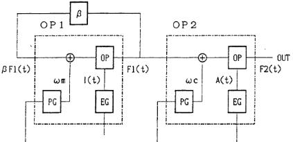
Figure 2-2 is a block chart of two operators FM that is the basic configuration of FM method.
β: Self feedback
Frequency |
Envelope |
Frequency |
Envelope |
Data |
Data |
Data |
Data |
Figure 2-2: Two operator FM
In Figure 2-2, βis a return rate of the self feedback. The self feedback is a method to feed back the output of modulator as a modulation input. The output of OP1 is shown in the expression .
F1(t)=I(t)sin (ωmt+βF1(t)) |
..... |
Because feedback FM is equivalent to the connection of the operator to the series, and the overtone element becomes the harmonic component of the next integer as a result, it is suitable for the tone making a saw blade shape of waves (saw tooth wave) seen in the stringed instrument etc.
FM method can be expressed above by the expression of . And, a wider sound making is enabled by these combinations. This connection status is called an algorithm (connection). The OPNA connects four operators a sound (1CH). Four operator FM method is adopted, and it will select it from eight kinds of algorithms.
2-1-2: Parameters
When a current thing is brought together, it will only have to set the sound creation of the FM sound source as follows.
o Selection of algorithm
oPG (phase generator) parameter is set, and frequency information is given to the operator.
oEG (envelope generator) parameter is set, and envelope information is given to the operator.
o Setting of β in feedback FM.
The parameter is set by writing data in each register of the FM sound source part.
16
The parameter that controls each block of operators is as follows.
• |
Parameter concerning algorithm |
:Algorithm (Connection), Self-Feedback |
• |
PG parameter |
:Multiple, Detune, F-numbers, Block |
• |
EG parameter |
:TotalLevel, |
|
|
Attack Rate, Decay Rate, Sustain Rate, |
|
|
Sustain Level, Release Rate, SSG-Type EG, |
|
|
Key Scale |
• |
LFO parameter |
:FREQ.CONTROL(LFO SPEED), AMS, PMS, AMON |
2-1-3: Channel and slot
OPNA can pronounce 6 sounds (6 channels) at the same time. And, 24 operators in total will be multiplying because they need it by four operators a sound. However, this is a figure for convenience' sake because the FM sound source is understood conceptual, and has only one unit operator cell in LSI. As actual operation of the FM sound source, the operator cell is operated 24 times by the timesharing processing, and six sound pronunciation simultaneously becomes possible.
The state of the operator on the axis of time is expressed in the serial because it operates it like this as the slot. Thereafter, it treats as sound = channel and operator = slot.
17
Loading...