


LED COLOUR TV
MAINTENANCE MANUAL
CHASIS: HLS49J MSD308B
MODEL: LED32HTC2000E
(JUC7.820.00084054)
Please read this manual carefully before maintenance

Chapter1 Safety and notes.......................................................................................................................................................... |
3 |
1-1 Installation notes.......................................................................................................................................................... |
3 |
1-2 Attention points of operation and using ....................................................................................................................... |
3 |
1-3 Storage notes................................................................................................................................................................ |
3 |
1-4 Dismantling notes ........................................................................................................................................................ |
3 |
1-5 High-voltage warning .................................................................................................................................................. |
4 |
Chapter2 whole machine standard and terminal functions ........................................................................................................ |
4 |
2-1 Basic standard.............................................................................................................................................................. |
4 |
2-2 Introduction of terminals(practicality photos) ............................................................................................................. |
5 |
Chapter3 Main chip functions and the introductions of power supply ...................................................................................... |
6 |
3-1 Main IC and functions of HLS49J............................................................................................................................... |
6 |
3-2 Pin function description of HLS49J chip..................................................................................................................... |
7 |
3-2-1 MSD308B recommended operating power conditons................................................................................... |
7 |
3-2-2 M25P16 16Mbit(2M x 8bit) brief introduction: ............................................................................................ |
7 |
3-2-3 SY8009B DC-DC brief introduction:......................................................................................................... |
7 |
3.3 Brief introduction of power supply .............................................................................................................................. |
8 |
Chapter4 The chassis frame diagram, mainboard power supply systems, mainboard interface definition................................ |
8 |
4-1 Power supply system ................................................................................................................................................... |
9 |
4-1-1 The composition and distribution of the TV power supply .............................................................................. |
9 |
4-1-2 Pin voltage of the voltage adjustor on the mainboard .................................................................................... |
10 |
4-1-3 Interface definition ......................................................................................................................................... |
11 |
Chapter5 Software upgrade instructions .................................................................................................................................. |
11 |
5-1 Software upgrade tooling---there are two kinds of using upgrade tooling ................................................................ |
11 |
5-2 Software upgrade introduction................................................................................................................................... |
12 |
Chapter6: Classical accident maintenance procedures and examples...................................................................................... |
16 |
6-1 The thinking of don’t boot ......................................................................................................................................... |
16 |
6-2 Common problems for your reference....................................................................................................................... |
16 |
Chapter7 High voltage and high current wearing parts list...................................................................................................... |
17 |
Chapter8 Factory mode parameter setting instructions and notes............................................................................................ |
17 |
8-1 Enter into the factory mode ....................................................................................................................................... |
17 |
8-2 Setting method of factory menu................................................................................................................................. |
19 |
Chapter9 Instructions of HLS49J module Circuit Schematic Diagram ................................................................................... |
20 |
Appendix Circuit Schematic Diagram .............................................................................................................................. |
20 |

Chapter1 Safety and notes
1-1 Installation notes
(1)Please don't beat or rub, scratch the surface of the LED screen heavily, don’t touch it with your hand casually.
(2)When the screen is dirty, please clean it with absorbent cotton or cotton cloth slightly.
(3)Please clean it timely when water or other viscosity pollution fall, which may make the LED face or color change.
(4)Please don’t make the LED screen shaked by strong external force.
1-2 Attention points of operation and using
(1)Please unplug the power cable before moving the LED screen.
(2)Please don’t change the original setting of the mainboard’s, if not, the brightness and white balance etc. may not meet the specification.
(3)The radiation of a long time using in the room temperature is larger than the low temperature.
(4)Please note that the long displaying image may remain at the top when shutdown the machine.
(5)Please avoid the impact from the mobile phone to protect your TV.
1-3 Storage notes
(1)When stored for a long time, please keep the temperature between 0 to 40 ,don’t expose the TV to the strong sunlight, the humidity should be less than 85 RH.
(2)Please don’t put your TV under high humidity and high temperature environment, for example, the temperature: 60 , and the humidity: 85%RH.
(3)Please don’t put your TV under low temperature environment, for example, the temperature lower than -25 .
1-4 Dismantling notes
(1)As LED screen is easy to be damaged, while dismantle, please attention to protect.
(2)Please attention the position of each screw when dismantle, in case to beat the wrong position when install, if not, it may lead to crack or slide of the face frame.
(3) If you need to dismantle the power board or the mainboard, please attention the position and

direction of each line, especially the direction of the screen line, in case of causing accident when install. Before dismantle, we can take some photos of the line route for the comparison of installing.
(4)After check and maintenance, please assure that there is no foreign body in the machine when install.
1-5 High-voltage warning
The high-voltage of the LED screen is generated by the power supply board, without attention to exposure to the high voltage, one may meet a serious electricity shock.
Chapter2 whole machine standard and terminal functions
2-1 Basic standard
|
Item |
Standard |
|
|
|
|
|
|
|
|
|
|
Model Name |
M320X13-E1-A(G3) |
|
|
|
|
visual area |
32 inches opposite angles |
|
|
|
|
aspect ratio |
16:9 |
|
|
|
|
resolving ratio |
1,366x768 Pixel |
|
the parameters |
are for |
|
visual area H x V |
697.685(H) x 392.256(V) |
|
||
|
|
reference only,the |
specific |
||
|
display colour |
8 bit, 16.7M million |
|
||
LED Panel |
|
should accord to the standard |
|||
Contrast Ratio |
3000 1 |
|
of the screen practicality of |
||
|
brightness |
280cd/m² |
|
the batch orders |
|
|
visual angle |
178°(horizontal)/178° (vertical) |
|
|
|
|
|
|
|
|
|
|
react time |
6.5ms |
|
|
|
|
|
|
|
|
|
|
backlight life |
30000 hours |
|
|
|
|
|
|
|
|
|
|
color temperature |
cold/hot |
|
|
|
|
|
|
|
|
|
TV function |
sound system |
B/G D/K I L |
|
|
|
color system |
PAL / SECAM |
|
|
|
|
|
|
|
|
||
|
AV |
AV x 1 |
Audio L/R x 1 |
|
|
|
aberration signal |
YPbPr x 1 |
support to1080P Audio L/R x 1, |
||
|
HDMI |
HDMI x3 |
support to1080P |
|
|
Audio and video |
USB |
USB x1 |
support media player |
|
|
|
plug and use |
|
|
|
|
signal input |
|
|
|
|
|
|
input frequency |
H: 31.5K -50KHz |
|
||
|
|
|
|||
|
PC input |
V: 60Hz |
|
||
|
|
|
|||
|
|
recommend |
1280x768(60HZ) |
|
|
|
|
Phone x 1 |
PC audio input |
|
|
Video output |
|
Output CVBS signal |
Output TV and AV signal ,Audio L/R x |
||
|
1 |
|
|
||
|
|
|
|
|
|
Audio output |
|
Audio output L / R |
8W inner speakers for each channel |
||
Power |
power supply |
AC100V~240V, 50/60Hz |
|
power achievement |
<150W |
||
|
|||
|
operation temperature |
+ 0° ~ + 40° |
|
requirement for environment |
storage temperature |
- 20 ° ~ + 60° |
|
|
operation humidity |
10% ~ 85% |
|
appearance size |
W x H x D |
|
|
|
|
|
|
net weight |
no accessory |
Kg |
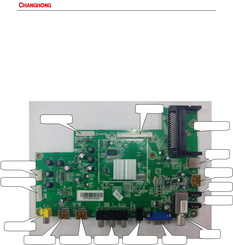
2-2 Introduction of terminals(practicality photos)
Lvds output
Power input
PCMCIA Card Slot
USB input
Audio output
HDMI3 input
Keypad IR input
AV input
YPBPR input
Coaxial output
RF input
HDMI2 input |
HDMI1 input |
AV out |
PC audio input |
PC input |
ATTENTION:
1.HDMI and YPbPr support to 1080P
2.The recommendation resolving ratio of PC is 1280X768
Chapter3 Main chip functions and the introductions of power supply
3-1 Main IC and functions of HLS49J
No. |
Item no. |
Model(EXAMPLE) |
Main function |
1 |
U001 |
AMS1117/A-3.3 |
5V to 3.3V LDO |
2 |
U200 |
MSD308B |
Video decoder, image processor, A/D and D/A conversion |
3 |
U201 |
H5TQ1G63DFR-PBC |
DDR3 |
4 |
U205 |
EN25Q64-104HIP |
64Mbit(8M x8bit), low voltage, Serial Flash memory |
5 |
U804 |
AMS1117/A-3.3 |
5V to 3.3V LDO |
6 |
U805 |
AMS1117/A-3.3 |
5V to 3.3V LDO |
7 |
U809 |
SY8009B |
5V to 1.15V DC-DC |
8 |
U808 |
AMS1117/A-1.5 |
5V to 1.5V LDO |
9 |
U700 |
RT9108NBGCP |
Power amplifier |
10 |
A002 |
DT21WN-2A-E |
Silicon high frequency head integrated chips |
11 |
U806 |
MP1471 |
12V to 5V DC-DC |
12 |
UT001 |
MSB101A |
DVBT2 DEMO |
13 |
UT002 |
AMS1117/A-3.3 |
5V to 3.3V LDO |
14 |
UT003 |
AMS1117-ADJ |
5V to 1.2V LDO |
15 |
UT004 |
EN25F40-100GCP |
4M-bit (512K-byte) |
U808 LDO-1.5V
U201 DDR3
UT002 LDO-3.3V
U806:MP1471 |
U200 MSD309B |
UT004 Flash Memory
U809: DC-DC-1.15V
UT001 MSB101A
U700 RT9108NBGCP
UT003 LDO-1.2V
U805 LDO-3.3V
U205:Flash Memory
U804 LDO-3.3V
U001 LDO-3.3V
A002: TDA18273HNDT21WN-2A-E
3-2 Pin function description of HLS49J chip
3-2-1 MSD308B recommended operating power conditons
(The Main Chip cancel 1.8V Supply Voltages because of DDR3 supplied by 1.5V )
Parameter |
Symbol |
Min |
Typ |
Max |
Unit |
3.3STB Supply Voltages |
VvDD_33 |
3.14 |
3.3 |
3.46 |
V |
3.3V Supply Voltages |
VvDD_33 |
3.14 |
3.3 |
3.46 |
V |
1.5V Supply Voltages |
VvDD_15 |
1.43 |
1.5 |
1.57 |
V |
1.15V Supply Voltages |
VvDD_1v15 |
1.09 |
1.15 |
1.21 |
V |
2.5V Supply Voltages |
VvDD_25 |
2.38 |
2.5 |
2.62 |
V |
1.2V Supply Voltages |
VvDD_12 |
1.14 |
1.2 |
1.26 |
V |
Junction Temperature |
Tj |
|
|
125 |
|
Case Temperature |
TC |
|
|
100 |
|
3-2-2 EN25Q64-104HIP 64Mbit(8M x 8bit) brief introduction:
Pin NO. |
Pin Name |
I/O |
Function |
|
1 |
CS# |
I |
Chip Select |
|
2 |
SO |
O |
Serial |
Data Output |
3 |
WP# |
I |
White Protect |
|
4 |
Vss |
|
Ground |
|
5 |
SI |
I |
Serial |
Data Input |
6 |
SCK |
I |
Serial Clock |
|
7 |
HOLD# |
I |
Power Supply |
|
8 |
VDD |
|
Power Supply |
|
3-2-3 SY8009B DC-DC brief introduction:
Pin introduction: |
|
|
|
|
Function description |
Pin |
SYMBOL |
|
1 |
EN |
Enable Input. |
2 |
GND |
Ground |
3 |
OUT |
Power Switching Output. |
4 |
IN |
DC Power Input. |
5 |
NC |
Not Connect |
6 |
FB |
Feedback Input. |

3.3 Brief introduction of power supply
Use for mainbord |
PS-ON |
power supply. |
DIM |
|
BL-ON |
|
GND |
|
GND |
|
GND |
|
GND |
|
12V |
|
12V |
|
12V |
|
|
Use for LED backlight power supply.
AC input AC100-240V 50/60HZ
Chapter4 The chassis frame diagram, mainboard power supply systems,
mainboard interface definition
This chapter mainly introduce the chassis frame diagram, power supply system, interface definition
 Loading...