


XR-L500
Table of contents
 Loading...
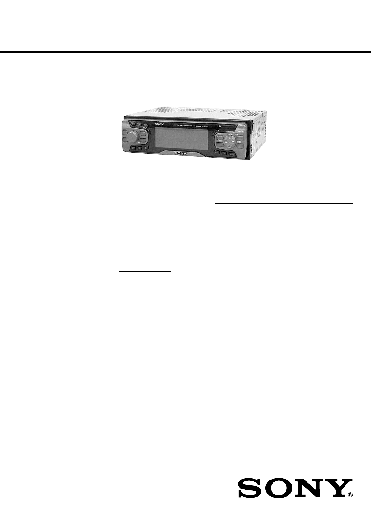
XR-L500/L500V/L500X
SERVICE MANUAL
Ver 1.1 2001.05
Photo: XR-L500
SPECIFICATIONS
Cassette Player section
Tape track 4-track 2-channel stereo
Wow and flutter 0.08 % (WRMS)
Frequency response 30 – 18,000 Hz
Signal-to-noise ratio
Cassette type
TYPE II, IV 61 dB
TYPE I
Tuner section
FM
Tuning range 87.5 – 108.0 MHz
Aerial terminal External aerial connector
Intermediate frequency 10.7 MHz/450 kHz
Usable sensitivity 8 dBf
Selectivity 75 dB at 400 kHz
Signal-to-noise ratio 66 dB (stereo),
Harmonic distortion at 1 kHz
Separation 35 dB at 1 kHz
Frequency response 30 – 15,000 Hz
MW/LW
Tuning range MW: 531 – 1,602 kHz
Aerial terminal External aerial connector
Intermediate frequency 10.7 MHz/450 kHz
Sensitivity MW: 30 µV
72 dB (mono)
0.6 % (stereo),
0.3 % (mono)
LW: 153 – 279 kHz
LW: 40 µV
58 dB
AEP Model
UK Model
Model Name Using Similar Mechanism XR-4300R
T ape Transport Mechanism Type MG-25G-136
General
Outputs Audio outputs (Rear)
Inputs Telephone ATT cont ro l lead
Tone controls Bass ±8 dB at 100 Hz
Loudness 100 Hz +8 dB
Power requirements 12 V DC car battery
Dimensions Approx. 178 × 50 × 176
Mounting dimensions Approx. 182 × 53 × 161
Mass Approx. 1.2 kg
Supplied accessories Parts for installation and
Note
This unit cannot be connected to a digital preamplifier
or an equalizer.
Design and specifications are subject to change
without notice.
Power aerial relay control
lead
Power amplifier con trol lead
Remote controller input
connector
Aerial input connector
Treble ±8 dB at 10 kHz
10 kHz +2 dB
(negativ e eart h )
mm (w/h/d)
mm (w/h/d)
connections (1 set)
Front panel case (1)
Power amplifier section
Outputs Speaker outputs
Speaker impedance 4 – 8 ohms
Maximum power output 50 W × 4 (at 4 ohms)
(sure seal connectors)
FM/MW/LW CASSETTE CAR STEREO
9-870-247-12 Sony Corporation
2001E0500-1 e Vehicle Company
C 2001.5 Shinagawa Tec Service Manual Production Group

SECTION 4
frequency counter
test tape
WS-48A
(3 kHz, 0 dB)
set
AUDIO OUT REAR jack (CNJ151)
–
+
10 kΩ
MECHANICAL ADJUSTMENTS
XR-L500/L500V/L500X
SECTION 5
ELECTRICAL ADJUSTMENTS
1. Clean the following parts with a denatured-alcohol-moistened
swab:
playback head pinch roller
rubber belt capstan
idler
2. Demagnetize the playback head with a head demagnetizer.
3. Do not use a magnetized screwdriver for the adjustments.
4. The adjustments should be performed with the power supply
voltage (14.4 V) unless otherwise noted.
• T orque Measurement
Mode Torque Meter Meter Reading
Forward CQ-102C (30 – 65 g•cm)
Forward
Back Tension
Reverse CQ-102RC (30 – 65 g•cm)
Reverse
Back Tension
FF, REW CQ-201B (60 – 200 g•cm)
CQ-102C (0.5 – 4.5g•cm)
CQ-102RC (0.5 – 4.5g•cm)
2.95 – 6.37 mN•m
(0.42 – 0.90 oz•inch)
0.05 – 0.44 mN•m
(0.01 – 0.06 oz•inch)
2.95 – 6.37 mN•m
(0.42 – 0.90 oz•inch)
0.05 – 0.44 mN•m
(0.01 – 0.06 oz•inch)
5.89 – 19.61 mN•m
(0.83 – 2.78 oz•inch)
• T ape Tension Measurement
Mode Tension Meter Meter Reading
Forward CQ-403A
Reverse CQ-403R
more than 60 g
(more than 2.12 oz)
more than 60 g
(more than 2.12 oz)
TAPE DECK SECTION
0 dB=0.775 V
Tape Speed Adjustment
Setting:
Procedure:
1. Put the set into the FWD PB mode.
2. Adjust adjustment resistor for inside capstan motor so that the
reading on the frequency counter becomes 3,000 Hz.
Specification: Constant speed
Frequency counter
2,955 to 3,075 Hz
Adjustment Location:
– SET UPPER VIEW –
Tape Speed Adjustment
TUNER SECTION
Tuner section adjustments are done automatically in this set.
13
XR-L500/L500V/L500X
SECTION 6
DIAGRAMS
6-1. NOTE FOR PRINTED WIRING BOARDS AND SCHEMATIC DIAGRAMS
Note on Printed Wiring Board:
• X : parts extracted from the component side.
• Y : parts extracted from the conductor side.
• : Pattern from the side which enables seeing.
(The other layers' patterns are not indicated.)
Caution:
Pattern face side: Parts on the pattern face side seen from
(Conductor Side) the pattern face are indicated.
Parts face side: Parts on the parts face side seen from
(Component Side) the parts face are indicated.
Note on Schematic Diagram:
• All capacitors are in µF unless otherwise noted. pF: µµF
50 WV or less are not indicated except for electrolytics
and tantalums.
• All resistors are in Ω and 1/
specified.
• C : panel designation.
• A : B+ Line.
• Power v oltage is dc 14.4V and fed with regulated dc power
supply from ACC and BATT cords.
• Voltages and waveforms are dc with respect to ground
under no-signal (detuned) conditions.
no mark : FM
( ) : MW/LW
〈〈 〉〉 : TAPE PLA YBACK
• Voltages are tak en with a V OM (Input impedance 10 MΩ).
Voltage variations may be noted due to normal production tolerances.
• Waveforms are taken with a oscilloscope.
Voltage variations may be noted due to normal production tolerances.
• Circled numbers refer to waveforms.
• Signal path.
F : FM
f : MW/LW
E : T APE PLA YBA CK
L : BUS AUDIO IN
: Impossible to measure
∗
4
W or less unless otherwise
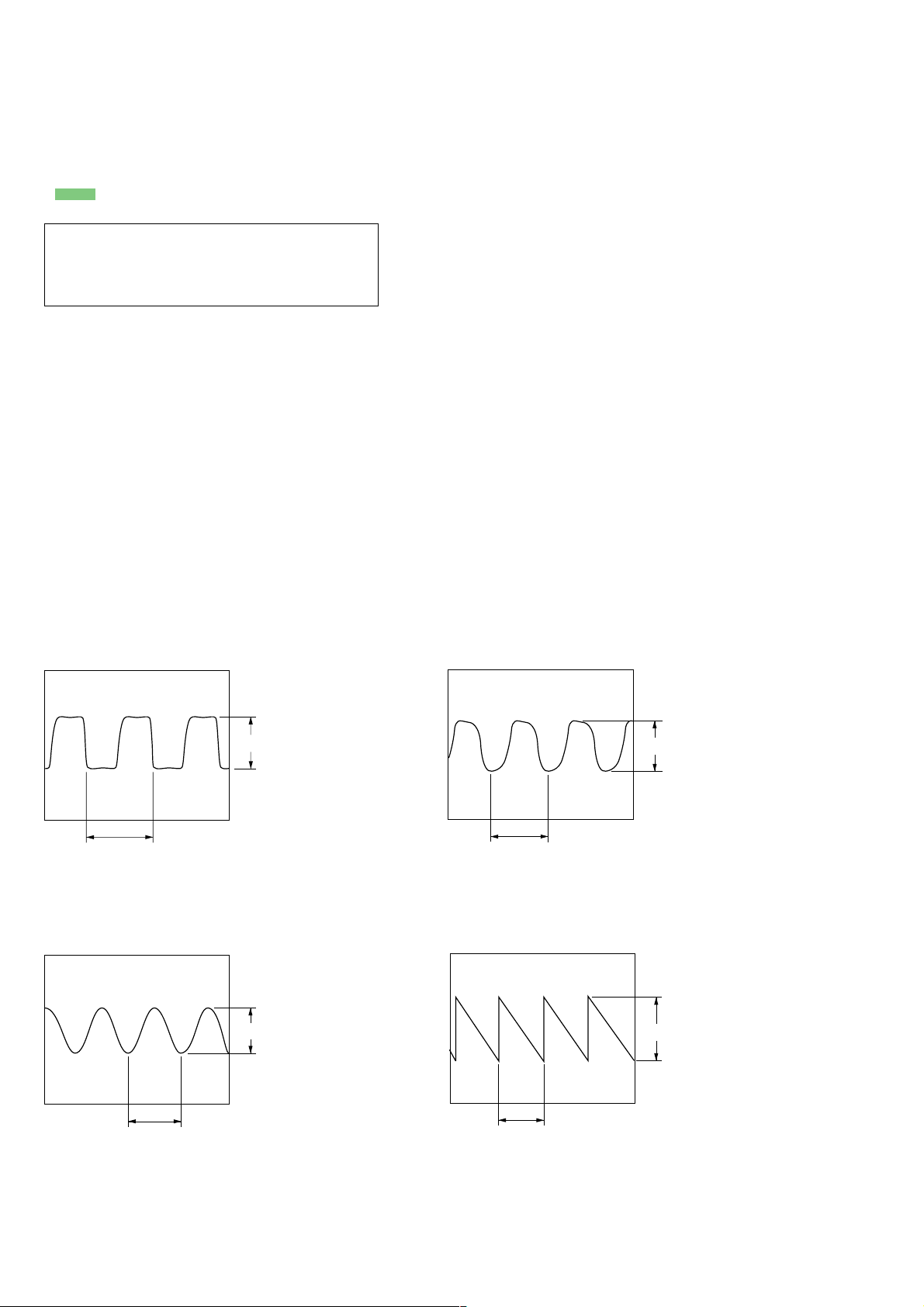
• Waveforms
– MAIN Board –
1 IC51 4 (OSCO)
232 ns
2 IC501 qs (OSCOUT)
5 Vp-p
3.3 Vp-p
3 IC501 qh (XOUT)
5 Vp-p
30.8 µs
– KEY Board –
4 IC900 uf (OSC)
2.5 Vp-p
14
54.4 ns
22.4 µs

XR-L500/L500V/L500X
6-3. SCHEMATIC DIAGRAM – MAIN Board (1/3) – • See page 14 for Waveform. • See page 23 for IC Block Diagrams.
(Page 17) (Page 18)
1616
6-4. SCHEMATIC DIAGRAM – MAIN Board (2/3) – • See page 14 for Waveforms. • See page 23 for IC Block Diagrams.
XR-L500/L500V/L500X
(Page 16)
(Page 18)
1717
Loading...