


HT-BE1
Table of contents
 Loading...
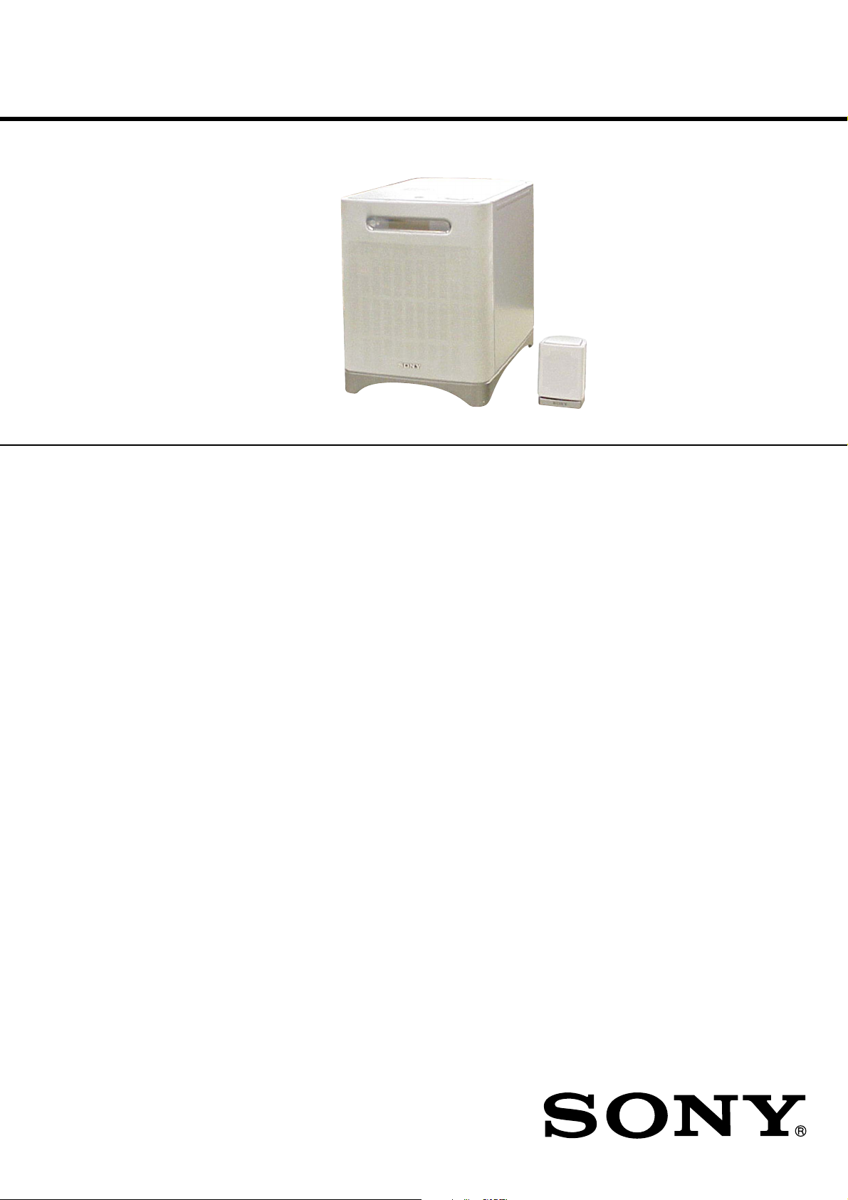
HT-BE1/SA-WBE1/SS-BE1
SERVICE MANUAL
Ver 1.2 2003. 08
The HT-BE1 system consists of one unit
of SA-WBE1 and five units of SS-BE1.
This system incorporates Dolby* Digital and Pro Logic Surround and
the DTS** Digital Surround System.
* Manufactured under license from Dolby Laboratories.
“Dolby,” “Pro Logic,” and the double-D symbol are trademarks of
Dolby Laboratories.
Confidential unpublished works. © 1992-1997 Dolby Laboratories. All
rights reserved.
** Manufactured under license from Digital Theater Systems, Inc. US Pat.
No. 5,451,942 and other worldwide patents issued and pending. “DTS”
and “DTS Digital Surround” are trademarks of Digital Theater Systems,
Inc. © 1996 Digital Theater Systems, Inc. All rights reserved.
SA-WBE1
US Model
Canadian Model
AEP Model
UK Model
E Model
SS-BE1
SPECIFICATIONS
AUDIO POWER SPECIFICATIONS
POWER OUTPUT AND TOTAL HARMONIC DISTORTION:
With 6 ohm loads, both channels driven, from 120 – 10,000 Hz; rated 19
watts per channel minimum RMS power, with no more than 10 % total
harmonic distortion from 220 milliwatts to rated output.
SA-WBE1 (subwoofer)
Max. output
Subwoofer: 30 W (6 ohms)
Front: 15 W + 15 W (6 ohms)
Center*: 15 W
Rear*: 15 W + 15 W
* Depending on the sound field settings and the source, ther e may be no sound output.
Speaker system Bass reflex type
Speaker unit 130 mm (5 1/8 inches) dia. cone type
Dimensions (approx.) 215 × 271 × 302 mm (8 1/2 × 10 3/4 × 12 inches)
(w/h/d, not including the projecting parts)
Mass (approx.)
US, CND model: 6.3 kg (13 lb 15 oz )
AEP, UK, SP, MY model: 6.4 kg (14 lb 2 oz )
SS-BE1 (satellite speakers)
Speaker system Closed box type
Speaker unit 50 mm (2 inches ) dia. cone type
Rated impedance 6 ohms
Dimensions (approx.) 61 × 82 × 65.5 mm (2 1/2 × 3 1/4 × 2 5/8 inches) (w/h/d)
Mass (approx.) 175 g (7 oz)
General
Power requirements
US, CND, MX model: 120 V AC, 60 Hz
AEP, UK model: 230 V AC, 50/60 Hz
SP, MY model: 220-240 V AC, 50/60 Hz
Power consumption
US model: 60 W
1.0 W (at the Power Saving Mode)
CND, MX model: 75 W
1.0 W (at the Power Saving Mode)
AEP, UK, SP, MY model: 45 W
0.3 W (at the Power Saving Mode)
Operating temperature 5°C to 35°C (41°F to 95°F)
Operating humidity 5 % to 90 %
Supplied accessories Speaker cords (3 m (10 ft) × 3, 8 m (26 ft) × 2)
Optical digital cord (1) (US, CND, SP, MY model)
Coaxial digital cord (1) (AEP, UK model)
Remote commander (remote) RM-BE1 (1)
Size AA (R6) batteries (2)
Design and specifications are subject to change without notice.
•Abbreviation
CND : Canadian model
SP : Singapore model
MY : Malaysia model
MX : Mexican model
HOME THEATER SYSTEM
9-874-031-03
2003H04-1
© 2003. 08
Sony Corporation
Home Audio Company
Published by Sony Engineering Corporation
1
HT-BE1/SA-WBE1/SS-BE1
SAFETY CHECK-OUT
After correcting the original service problem, perform the following
safety check before releasing the set to the customer:
Check the antenna terminals, metal trim, “metallized” knobs, screws,
and all other exposed metal parts for AC leakag e. Check leakage as
described below.
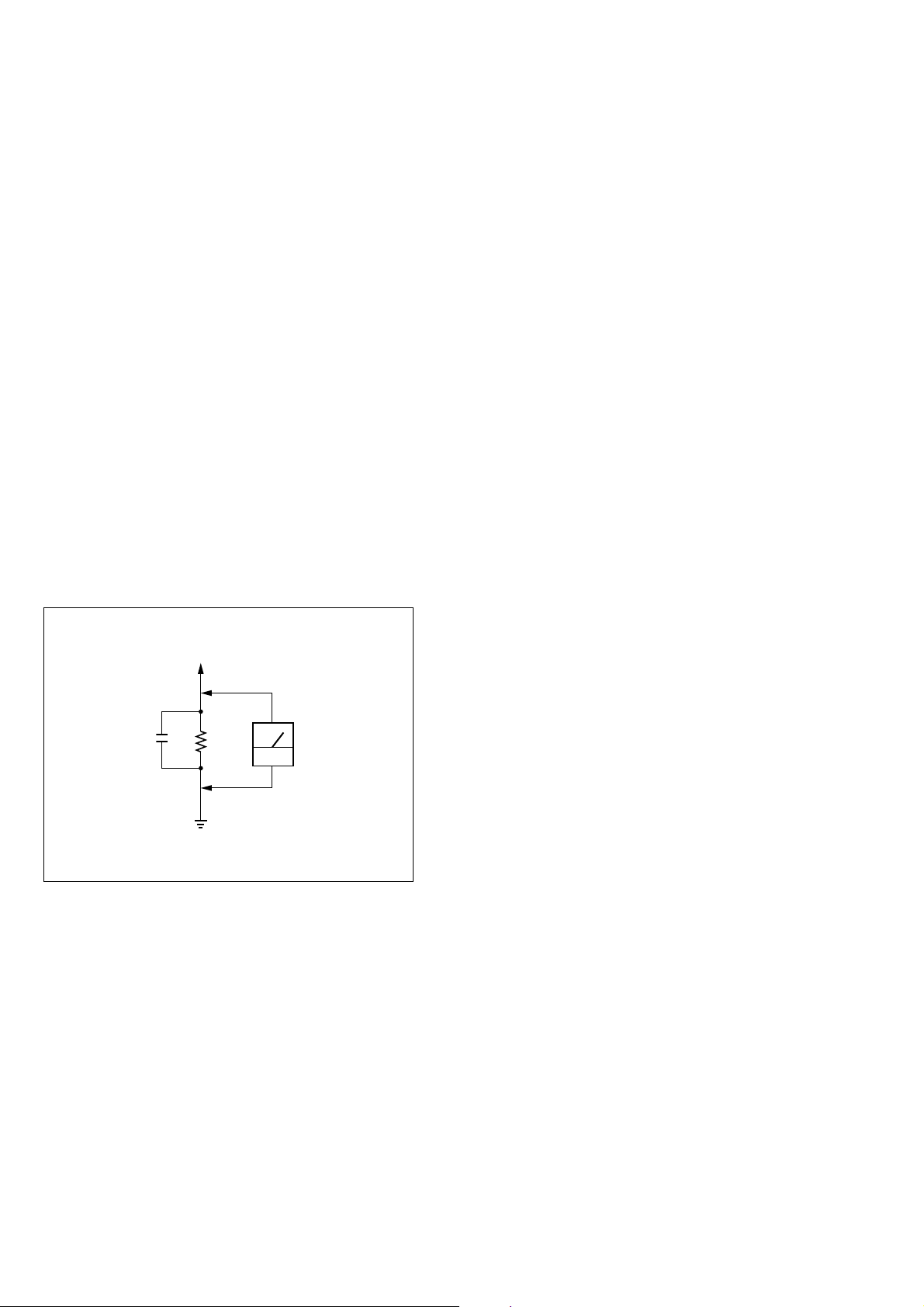
LEAKAGE TEST
The AC leakage from any exposed metal part to earth ground and
from all exposed metal parts to any exposed metal part having a
return to chassis, must not exceed 0.5 mA (500 microamperes).
Leakage current can be measured by any one of three methods.
1. A commercial leakage tester, such as the Simpson 229 or RCA
WT-540A. Follow the manufacturers’ instructions to use these
instruments.
2. A battery-operated AC milliammeter. The Data Precision 245
digital multimeter is suitable for this job.
3. Measuring the voltage drop across a resistor by means of a V OM
or battery-operated AC voltmeter. The “limit” indication is 0.75
V, so analog meters must have an accurate low-v oltage scale. The
Simpson 250 and Sanwa SH-63Trd are examples of a passive
VOM that is suitable. Nearly all battery operated digital
multimeters that have a 2V AC range are suitable. (See Fig. A)
TABLE OF CONTENTS
1. SERVICING NOTE
1-1. Extension Cable and Service Position ................................ 3
2. GENERAL
Index to Parts and Controls .................................................4
3. DISASSEMBLY
3-1. Top Chassis Assy................................................................. 5
3-2. Display Board, Key Board .................................................. 6
3-3. Rear Panel Assy................................................................... 6
3-4. Main Board ......................................................................... 7
4. DIAGRAMS
4-1. IC Pin Descriptions ............................................................. 8
4-2. Block Diagram –Main Section–........................................ 12
4-3. Block Diagram –Power Section– ...................................... 13
4-4. Printed Wiring Board –Jack Section– ............................... 14
4-5. Schematic Diagram –Jack/Main (5/1) Section–................ 15
4-6. Printed Wiring Board –Main Section– .............................. 16
4-7. Schematic Diagram –Main (2/5) Section– ........................ 18
4-8. Schematic Diagram –Main (3/5) Section– ........................ 19
4-9. Schematic Diagram –Main (4/5) Section– ........................ 20
4-10. Schematic Diagram –Main (5/5) Section– ........................ 21
4-11. Schematic Diagram –Display/Key Section– ..................... 22
4-12. Printed Wiring Board –Display Section– .......................... 23
4-13. Printed Wiring Board –Key Section–................................ 24
4-14. IC Block Diagrams............................................................ 25
To Exposed Metal
Parts on Set
0.15µF
1.5k
Ω
Earth Ground
AC
voltmeter
(0.75V)
Fig. A. Using an AC voltmeter to check AC leakage.
SAFETY-RELATED COMPONENT WARNING!!
COMPONENTS IDENTIFIED BY MARK 0 OR DOTTED LINE
WITH MARK 0 ON THE SCHEMATIC DIAGRAMS AND IN
THE PARTS LIST ARE CRITICAL TO SAFE OPERATION.
REPLACE THESE COMPONENTS WITH SONY PAR TS WHOSE
PART NUMBERS APPEAR AS SHOWN IN THIS MANUAL OR
IN SUPPLEMENTS PUBLISHED BY SONY.
5. EXPLODED VIEWS
5-1. Main Section (SA-WBE1) ................................................ 28
5-2. Main Board Section (SA-WBE1) ..................................... 29
6. ELECTRICAL PARTS LIST......................................... 30
ATTENTION AU COMPOSANT AYANT RAPPORT
LES COMPOSANTS IDENTIFIÉS P AR UNE MARQUE 0 SUR LES
DIAGRAMMES SCHÉMATIQUES ET LA LISTE DES PIÈCES
SONT CRITIQUES POUR LA SÉCURITÉ DE FONCTIONNEMENT .
NE REMPLACER CES COMPOSANTS QUE PAR DES PIÈCES
SONY DONT LES NUMÉROS SONT DONNÉS DANS CE MANUEL
OU DANS LES SUPPLÉMENTS PUBLIÉS PAR SONY.
À LA SÉCURITÉ!!
2
HT-BE1/SA-WBE1/SS-BE1
A
SECTION 1
SERVICING NOTE
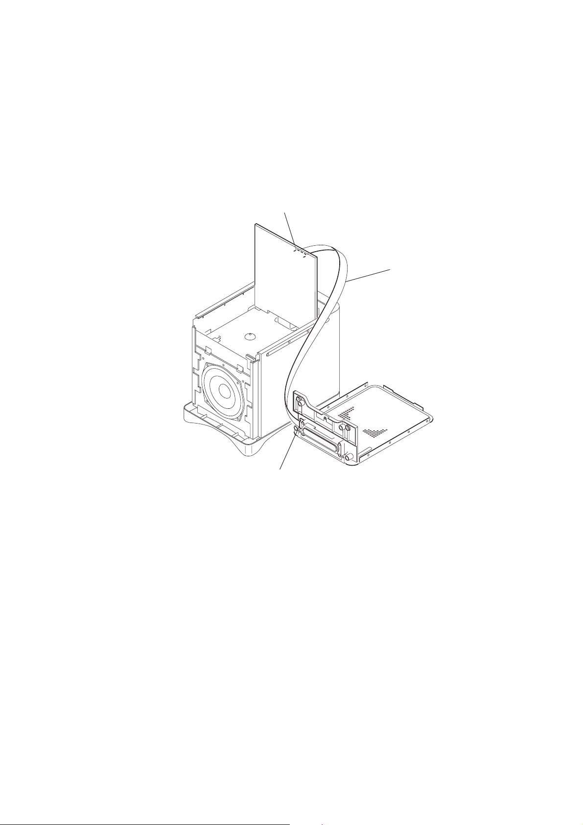
1-1. EXTENSION CABLE AND SERVICE POSITION
When repairing or servicing this set, connecting the jig (extension cable) as shown below.
• Connect the MAIN board (CN801) and the DISPLAY board (CN701) with the extension cable (Part No. J-2501-049-A).
MAIN board
(CN801)
J-2501-049-
DISPLAY board
(CN701)
3
HT-BE1/SA-WBE1/SS-BE1
SECTION 2
GENERAL
This section is extracted
from instruction manual.
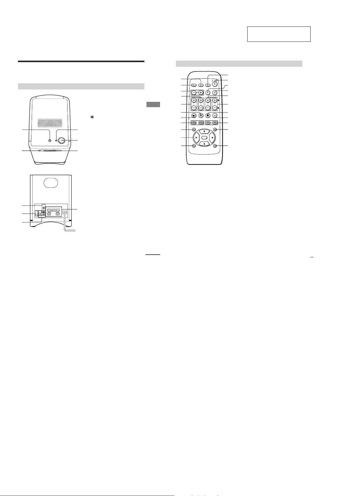
Index to Parts and Controls
Refer to the pages indicated in parentheses for details.
Subwoofer
1
2
6
7
L
SPEAKER
FRONT R CENTER
FRONT L
AUDIO IN
R
USB
OPTICAL COAXIAL
REAR R REAR L
DIGITAL IN
8
3
4
5
9
Top panel/Front panel
1 ?/1 (POWER) switch and indicator (15,
23)
Turns on and off the power of the
system.
remote sensor (5, 25)
2
Accepts the remote control signals.
3 MENU/ENTER (15, 16, 17, 19, 20, 23)
Displays the menu on the display
window. To executes the settings, press
this button again.
4 VOL/SELECT knob (15, 16, 17, 19, 20,
23)
Adjust the volume and select settings.
5 Display window (13, 15, 17)
Indicates the speaker setting, input
signal, sound field mode, etc.
Rear panel
6 AUDIO IN L/R jacks (11)
Connect to the audio output of a TV,
VCR, etc.
7 USB jack (11)
Connect to the PC.
8 DIGITAL IN OPTICAL/COAXIAL
jacks (10)
Connect to the DIGITAL OUT
(OPTICAL) jack of the DVD player, etc.
9 SPEAKER jacks (7)
Connect to the supplied satellite
speakers.
continued
Additional Information
GB
27
Remote
1
2
3
4
5
6
7
8
9
q;
qa
1 TV button (22)
Turns the TV on and off.
2 SHIFT button (13, 16, 19, 20, 22, 23)
Switches the function of the buttons on
the remote.
3 TV CH +/– (TV/VIDEO) buttons (22)
Changes the TV channel.
To change the TV input, press – while
pressing SHIFT.
4 REAR +/– buttons (16)
Adjust the rear speakers volume.
5 CENTER +/– buttons (16)
Adjust the center speaker volume.
6 XPA USE button (21)
Pauses playing a disc.
7 NPLAY button (21)
Plays a disc.
8 ./>PREV/NEXT buttons (21)
Press to go to the next chapter or track,
or to go back to the previous chapter or
track.
SHIFT
TV DVD1
TV CH
FUNCTION
VIDEO
TV/
LEVEL
CENTER
REAR
PLAY PAUSE
PREV NEXT SCAN
DVD TOP MENU
ENTER
DVD CONTROL
DVD2
SOUND
FIELD
MENU
WOOFER
VOLUME
STOP MUTING
TEST TONE
DVD MENU
RETURNDISPLAY
9 DVD TOP MENU button (21)
qs
qd
qf
qg
qh
qj
qk
ql
w;
wa
ws
Displays the title menu on the TV
screen.
0 </M/m/,/ENTER button (21)
Selects and executes the items or
settings.
qa DISPLAY button (21)
Displays the setup display of the DVD
player.
qs DVD 1/DVD 2 button (21)
Turns on and off the power of the DVD
player.
qd ?/1 (POWER) switch (13, 15)
Turns on and off the system.
qf FUNCTION button (15)
Selects the input signal.
qg SOUND FIELD (MENU) button (13,
17, 19, 20, 23)
Selects the sound field mode.
Pressing this button while pressing
SHIFT will select the menu.
qh WOOFER +/– buttons (16)
Adjust the subwoofer volume.
qj VOLUME +/– buttons (13, 15, 19, 20,
23)
Make the speaker settings or adjust the
volume of the system.
Pressing this button while pressing
SHIFT will set the speaker setup
parameters.
qk xSTOP button (21)
Stops playing a disc.
ql MUTING (TEST TONE) button (15,
16)
Mutes the sound.
Pressing this button while pressing
SHIFT will sound the test tone.
w; m/M (SCAN) buttons (21)
Locate a point while monitoring the
picture.
wa DVD MENU button (21)
Displays the DVD menu on the TV
screen.
ws RETURN button (21)
Returns to the previously selected
screen.
4
SECTION 3
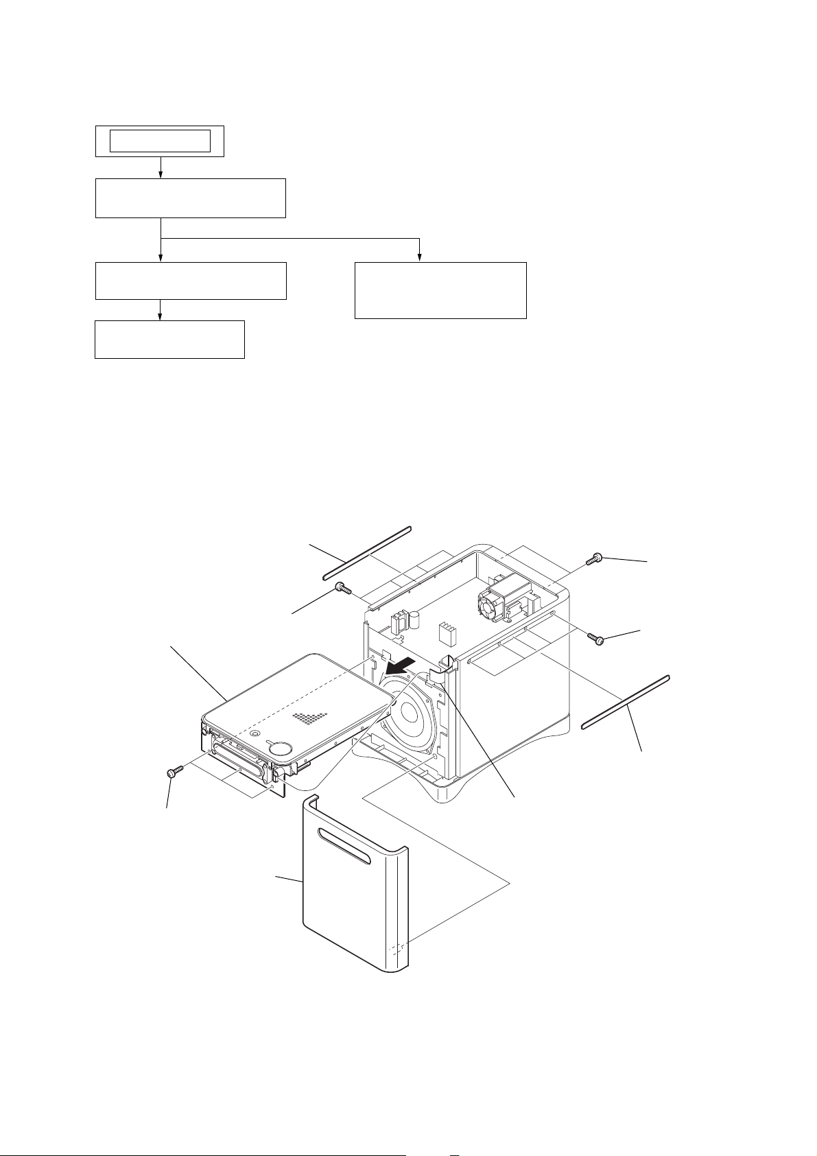
DISASSEMBLY
• The equipment can be removed using the following procedure.
SET
3-1. TOP CHASSIS ASSY
(Page 5)
HT-BE1/SA-WBE1/SS-BE1
3-3. REAR PANEL ASSY
(Page 6)
3-2. DISPLAY BOARD,
KEY BOARD
(Page 6)
3-4. MAIN BOARD
(Page 7)
Note : Follow the disassembly procedure in the numerical order given.
3-1. TOP CHASSIS ASSY
3
blind panel
4
BVTP 3x10
0
top chassis assy
9
5
BVTP 3x10
2
BVTP 3x10
8
BVTP 3x10
6
grille frame assy
7
CN701
1
blind panel
5
HT-BE1/SA-WBE1/SS-BE1
d
0
3-2. DISPLAY BOARD, KEY BOARD
7
DISPLAY board
5
CN702
6
BVTP 3x10
1
dial knob
9
KEY boar
3
BVTP 3x10
3-3. REAR PANEL ASSY
1
CN902
(Except US, Canadian, Mexican model)
1
CN901
(US, Canadian, Mexican model)
2
BVTP 3x10
2
CN381
4
LCD holder sub assy
3
CN383
4
CN301
8
BVTP 3x10
5
PTP 4x20
6
PTP 4x2
7
rear panel assy
6

3-4. MAIN BOARD
0
2
BVTP 3x10
9
MAIN board
7
4
CN421
5
BVTP 3x10
8
DC fan (FAN901)
BTP 3x25
HT-BE1/SA-WBE1/SS-BE1
3
BVTP 3x10
heat sink
1
CN382
6
BVTP 3x1
7
HT-BE1/SA-WBE1/SS-BE1
SECTION 4
DIAGRAMS
4-1. IC PIN DESCRIPTIONS
• IC801 µPD703033A (SYSTEM CONTROLLER)
Pin No. Pin Name I/O Pin Description
1 LRSY I CD L/R clock input
1 CO-DI O Data output for MAC.
2 CO-CLK O Clock output for MAC.
3U L/OTHER H I
4 USB L/OTHER H I USB setting input (Fixed at L)
5NC—Not used. (Open)
6 DSP-DO O Serial data output for DSP.
7 DIG-DI I Serial data input from DSP.
8 DIG-CLK O Clock output for DSP.
9 EVDD — Power supply pin (+3.3 V)
10 EVSS — Ground
11 DSP-RST O Reset signal output for DSP. (L: active)
12 DSP-PM O PLL initialization output for DSP.
13 DSP-CS O Chip select output for DSP.
14 DSP-HACN I Acknowledge signal input from DSP.
15 DSP-BST O Boot stop signal output for DSP.
16 DSP-GP9 I Decode signal input from DSP.
17 DSP-PLOCK I Internal PLL lock signal input from DSP.
18 DIR-ERR I PLL lock signal input from DIR.
19 DIR-CE O Chip enable signal output for DIR.
20 DIR-XST I Reset signal input from DIR.
21 VPP — Programming power supply pin
22 DIR-AD O Serial data output for DIR.
23 DIR-XMODE I System reset signal input from DIR.
24 DIRDO I Serial data input from DIR.
25, 26 NC — Not used. (Open)
27 MUTE-FL,FR O Amplifier mute (FL, FR) output
28 MUTE-SL,SR,C O Amplifier mute (SL, SR, C) output
29 MUTE-SW O Amplifier mute (SW) output
30 to 33 NC — Not used. (Open)
34 RESET I µ-com reset signal input
35 XT1 I Not used. (Fixed at L)
36 XT2 O Not used. (Open)
37 NC — Not used. (Connected to capacitor)
38 X2 O Main clock signal output (16 MHz)
39 X1 I Main clock signal input (16 MHz)
40 VSS — Ground
41 VDD — Power supply pin (+5 V)
42, 43 NC — Not used. (Open)
44 AMP-MUTE O Amplifier mute output
45 NC — Not used. (Open)
46 P-CONT I Power control signal input
47 to 50 NC — Not used. (Open)
51 DISC I Not used. (Fixed at L)
52 NC — Not used. (Open)
53 LCD-CLK O Clock output for LCD driver.
54 LCD-DATA O Serial data output for LCD driver.
55 LCD-CS O Chip select output for LCD driver.
56 LCD-C/D O Latch output for LCD driver.
57 LED-CLR — Not used. (Open)
Destination setting input (L: US, Canadian, Mexican model, H: Except US, Canadian,
Mexican model)
8
HT-BE1/SA-WBE1/SS-BE1
Pin No. Pin Name I/O Pin Description
58 BVDD — Power supply pin (+3.3 V)
59 BVSS — Ground
60, 61 NC — Not used. (Open)
62 READY-H O Power supply (ready) output
63 USB-PLYSCK I USB play/idle decision input
64 to 66 NC — Not used. (Open)
67 USB-H O USB/analog select output
68 VOL-STB O Latch output for volume control.
69 VOL-CLK O Clock output output for volume control.
70 VOL-DATA O Data output for volume control.
71 NC — Not used. (Open)
72 READY-H O Ready LED ON/OFF control output (ready mode: red LED light on)
73 NC — Not used. (Open)
74 AVDD — Analog power supply pin (+5 V)
75 AVSS — Analog ground
76 AVREF — Analog reference voltage pin (+5 V)
77 to 80 NC — Not used. (Fixed at H)
81 AUDIO DEC I Auto power ON/OFF level check input
82 KEY1 I Key AD value input
83 ENA I Encoder A input
84 ENB I Encoder B input
85 DIGITAL DEC I Level decision input from DIR.
86 to 88 NC — Not used. (Fixed at H)
89 NC — Not used. (Open)
90 STOP I Stop mode check signal input
91 SIRCS I SIRCS signal input
92 RDS-DATA I Not used. (Open)
93 P-WAKE I Interruption signal input from STOP mode.
94 to 96 NC — Not used. (Open)
97 IN I µ-com programming serial in input
98 CO-S/MUTE O Soft mute control output for MAC.
99 CO-PD O Soft reset control output for MAC
100 CO-CS O Chip select output for MAC.
9

HT-BE1/SA-WBE1/SS-BE1
• IC802 CXD9617R (DSP)
Pin No. Pin Name I/O Pin Description
1 VSS — Ground
2 XRST I Reset signal input from system controller.
3 EXTIN I Not used. (Connected to ground)
4 FS2 I Not used. (Connected to ground)
5 VDDI I Power supply pin (+2.4 V)
6 FS1 I Not used. (Connected to ground)
7 PLOCK O Internal PLL lock signal output for system controller.
8 VSS — Ground
9 MCLK1 I Clock signal input (13.5 MHz)
10 VDDI I Power supply pin (+2.4 V)
11 VSS — Ground
12 MCLK2 O Clock signal output (13.5 MHz)
13 MS I Switching signal input of master/slave operation. (Fixed at L : internal clock)
14 SCKOUT O Internal system clock signal output
15 LRCKI1 I Not used. (open)
16 VDDE I Power supply pin (+3.3 V)
17 BCKI1 I Not used. (open)
18 SDI1 I Audio IF data input
19 LRCKO O Sampling clock output for digital audio serial data
20 BCKO O Bit clock output for digital audio serial data
21 VSS — Ground
22 KFSIO I/O Audio clock signal (384fs/256fs) input/output
23 to 25 SDO1 to SDO3 O Digital audio serial data output
26 SDO4 O Audio IF serial output (Not used. (open))
27 SPDIF O Not used. (open)
28 LRCKI2 I Sampling clock input from audio serial data.
29 BCKI2 I Bit clock input from audio serial data.
30 SDI2 I Digital audio data input
31 VSS — Ground
32 HACN O Acknowledge signal output for system controller.
33 HDIN I Serial data input from system controller.
34 HCLK I Clock input from system controller.
35 HDOUT O Serial data output for system controller.
36 HCS I Chip select input from system controller.
37 SDCLK O Not used. (open)
38 CLKEN O Not used. (open)
39 RAS O Not used. (open)
40 VDDI I Power supply pin (+2.4 V)
41 VSS — Ground
42 CAS O Not used. (open)
43 DQM/OE0 O Not used. (open)
44 CS0 O External memory chip select output (SRAM) (Not used. (open))
45 WE0 O SRAM write enable output (Not used. (open))
46 VDDE I Power supply pin (+3.3 V)
47 WMD1 I Not used. (Fixed at L)
48 VSS — Ground
49 WMD0 I Not used. (Fixed at L)
50 PAGE2 O Not used. (open)
51 VSS — Ground
52 PAGE1 O External memory page switching signal output (Not used. (open))
53 PAGE0 O External memory page switching signal output (Not used. (open))
54 BOOT I Not used. (open)
10
HT-BE1/SA-WBE1/SS-BE1
Pin No. Pin Name I/O Pin Description
55 BTACT O Not used. (open)
56 BST I Boot stop signal input from system controller.
57 MOD1 I Operation mode signal input (Fixed at H : 256fs)
58 MOD0 I Operation mode signal input (Fixed at L : single chip mode)
59 EXLOCK I Lock signal input
60 VDDI I Power supply pin (+2.4 V)
61 VSS — Ground
62 to 66 A17 to A13 O External memory address output (SRAM) (Not used. (open))
67 GP10 O Connected to LRCKO
68 GP9 O Decode signal output for system controller.
69 GP8 I Audio signal input from DIR.
70 VDDI I Power supply pin (+2.4 V)
71 VSS — Ground
72 to 75 D15/GP7 to D12/GP4 I/O External memory data input/output (general port) (Not used. (open))
76 VDDE I Power supply pin (+3.3 V)
77 to 80 D11/GP3 to D8/GP0 I/O External memory data input/output (general port) (Not used. (open))
81 VSS — Ground
82 A9 O External memory address output (SRAM) (Not used. (open))
83 to 85 A12 to A10 O External memory address output (SRAM) (Not used. (open))
86 TDO O Not used. (open)
87 TMS I Not used. (open)
88 XTRST I Not used. (open)
89 TCK I Not used. (open)
90 TDI I Not used. (open)
91 VSS — Ground
92 to 97 A8 to A3 O External memory address output (SRAM) (Not used. (open))
98, 99 D7, D6 I/O External memory data input/output (SRAM) (Not used. (open))
100 VDDI I Power supply pin (+2.4 V)
101 VSS — Ground
102 to 105 D5 to D2 I/O External memory data input/output (SRAM) (Not used. (open))
106 VDDE I Power supply pin (+3.3 V)
107, 108 D1, D0 I/O External memory data input/output (SRAM) (Not used. (open))
109, 110 A2, A1 O External memory address output (SRAM) (Not used. (open))
111 VSS — Ground
112 A0 O External memory address output (SRAM) (Not used. (open))
113 PM I PLL initialization input from system controller.
114, 115 SDI3, SDI4 I Not used. (open)
116 SYNC I Sync/async selection input (Fixed at H : async)
117 to 119 VSS — Ground
120 VDDI I Power supply pin (+2.4 V)
Note on Schematic Diagram:
• All capacitors are in µF unless otherwise noted. pF: µµF
50 WV or less are not indicated except for electrolytics
and tantalums.
• All resistors are in Ω and 1/
specified.
• 2 : nonflammable resistor.
• C : panel designation.
Note:
The components identified by mark 0 or dotted
line with mark 0 are critical for safety.
Replace only with part
number specified.
• A : B+ Line.
•Voltage is dc with respect to ground under no-signal
(detuned) condition.
•Voltages are taken with a V OM (Input impedance 10 MΩ).
Voltage var iations may be noted due to normal production tolerances.
• Signal path.
F : LINE
c : DIGITAL AUDIO (OPTICAL)
J : DIGITAL AUDIO (COAXIAL)
•Abbreviation
CND : Canadian model.
SP : Singapore model.
MY : Malaysia model.
MX : Mexican model.
Note on Printed Wiring Boards:
• X : parts extracted from the component side.
• : Pattern from the side which enables seeing.
•Abbreviation
CND : Canadian model.
SP : Singapore model.
MY : Malaysia model.
MX : Mexican model.
4
W or less unless otherwise
Note:
Les composants identifiés par
une marque 0 sont critiques
pour la sécurité.
Ne les remplacer que par une
piéce portant le numéro
spécifié.
• Waveforms
1V/div 50nsec/div
1
12.0MHz
IC501 wk (XT0)
1V/div 50nsec/div
2
12.288MHz
IC803 wa (XOUT)
1V/div 20nsec/div
3
16.0MHz
IC801 ek (X2)
1V/div 50nsec/div
4
13.5MHz
IC802 qs (MCLK2)
1V/div 50nsec/div
5
13.5MHz
IC802 qf (SCKOUT)
3.0Vp-p
3.5Vp-p
2.6Vp-p
3.1Vp-p
4.0Vp-p
11 11
HT-BE1/SA-WBE1/SS-BE1
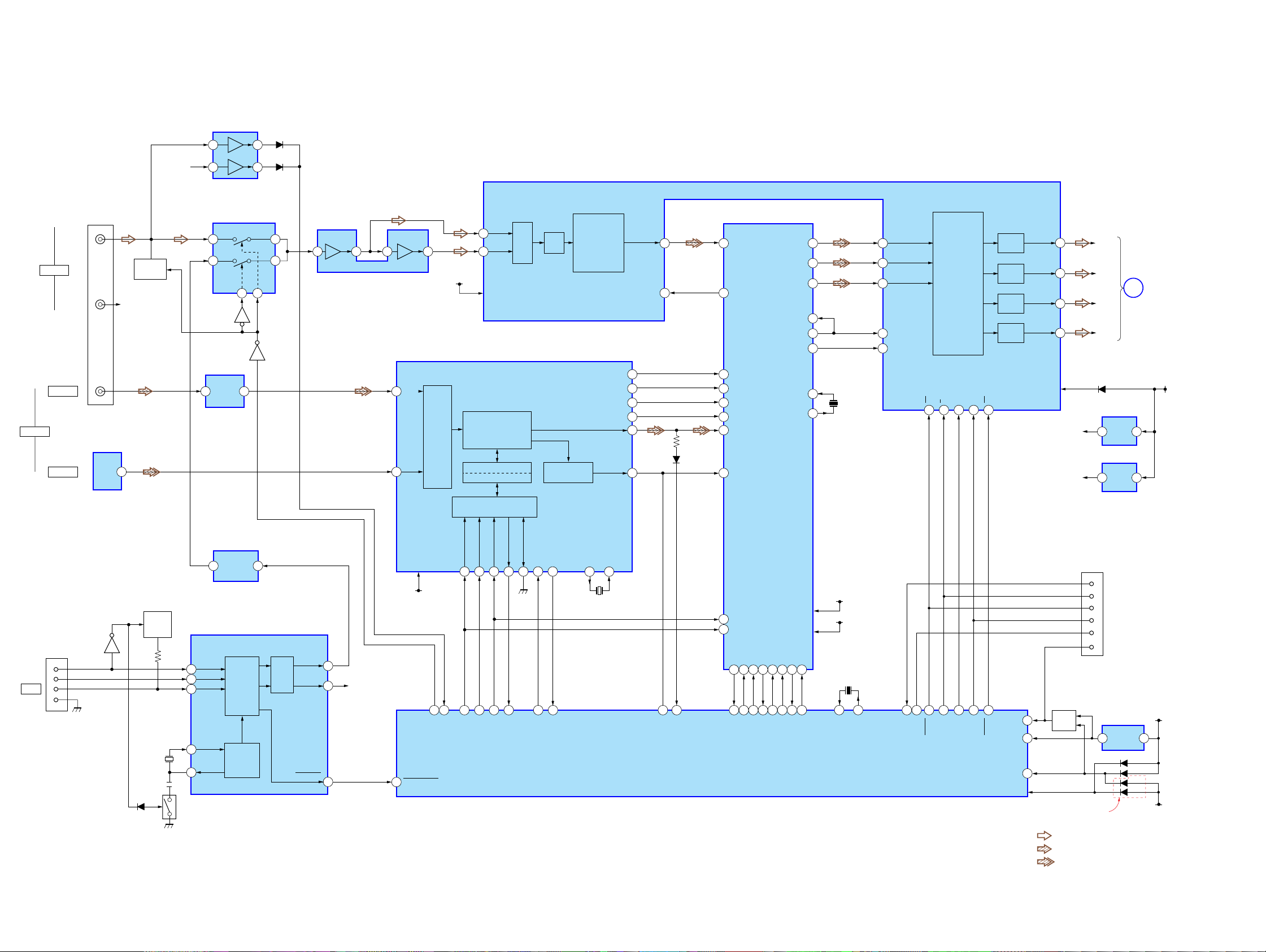
4-2. BLOCK DIAGRAM — MAIN SECTION —
AUDIO DETECT
IC505
6
R-CH
2
D507
7
D506
1
MULTI-CHANNEL
AUDIO CODEC
IC804
DIGITAL
AUDIO IN
COAXIAL
OPTICAL
L
R
J502
-1
-2
-3
OPTICAL
RECEIVER
IC503
OUT
1
R-CH
MUTE
Q504
INPUT SELECT
8
11
Q502
IC509
WAVE
SHAPER
IC502
12 6
23
Q501
DSP
DSI1
SCKOUTMCLKI
GP8
KFSIO
BCKI2
LRCKI2
SDI2
EXLOCK
IC802
SDO1
23 6
SDO2
24 7
SDO3
25 8
GP10
67
LRCKO
19 5
BCKO
20 4
MCLK1
9
MCLK2
12
X804
13.5MHz
SDTI1
SDTI2
SDTI3
LRCK
BCLK
AUDIO
PD
S/M
17
3 43 42 41
I/F
(2/2)
CDT1
CCLK
L-OUT
SL-OUT
C-OUT
SW-OUT
27
25
23
24
D5V
+2.5V
+3.3V
L
SL
C
SW
D510
+2.5V
REG
2 1
IC807
+3.3V
REG
3 2
IC808
A
POWER
SECTION
(Page 13)
READY
D5V
DAC
DAC
DAC
DAC
CS
LIN-
9
10
6 7 2 1
AMP
IC507
DIN0
3
DIN1
4
INPUT
29
30
AUDIO
5V
AVDD
DEMODULATOR
Pa,Pb DETECTION LOCK
C bit DETECTION
MICROPROCESSOR
ADC
LIN+
DIGITAL AUDIO
I/F RECEIVER
IC803
DATA
I/F
LPF
DETECTION
AUDIO
I/F
(1/2)
SDTO
9 18
39 14
24 69
AUDIO
13 22
CKOUT
14 29
BCK
15 28
LRCK
DATA
16 30
ERROR
D804
34 59
J501
USB
LPF
21
IC506
BIAS
D504
SWITCH
Q505
X501
12MHz
8
7
6
1
28
Q507
OSC
SWITCH
VBUS
DD+
XT1
XT0
Q506
USB
BUS
DETECT
1
VBUS
2
D-
3
D+
4
GND
USB INTERFACE,
D/A CONVERTER
IC501
USB
I/F
CRYSTAL
OSC
DAC
VOUTL
VOUTR
PLYBCK
23
19
R-CH
10
READY
63
USB-PLYSCK
VDD
+3.3V
CLCEDIDOBPSYNC
38 37 36 35 33 48 17
8 19 7 24 22 20
81
67
USB-H
AUDIO DEC
DIG-CLK
DIR-CE
DIG-DI
DIRDO
XMODE
DIR-AD
XSTATE
DIR-XST
XOUT
21 22
X803
12.288MHz
XIN
18
DIR-ERR
DIR-XMODE
33
HDIN
34
HCLK
GP9
68 56 2 11336 35 732
DSP-GP9
BST
HCS
151623 11 1213 6 1714
DSP-CS
DSP-BST
HACN
XRST
PM
DSP-RST
DSP-HACN
HDOUT
DSP-DO
DSP-PM
VDDI
VDDE
PLOCK
DSP-PLOCK
+2.5V
+3.3V
X801
16MHz
39 38
X1
X2
97
IN
SYSTEM
CONTROLLER
IC801 (1/2)
99 98 1 2 100
21
VPP
CO-PD
CO-S/MUTE
CO-DI
CO-CLK
OUT
2PIN
CLK
VPP
RESET
RESET
34
Q801
90 1 2
76
VDD
CO-CS
RESET
STOP
AVREF
• Signal path
8
IN
7
6
5
4
3
EXCEPT
US,CND,MX
MODEL
CN802
(PROGRAMMING)
RESET
IC806
D802
D803
D812
D811
D 5.6V
(SW)
D 5.6V
(UNSW)
: LINE
: DIGITAL AUDIO (COAXIAL)
: DIGITAL AUDIO (OPTICAL)
• R-ch is omitted due to
same as L-ch.
• Abbreviation
CND: Canadian model
1212
MX : Mexican model
Loading...