


PC815
High Sensitivity, High Density
PC815 Series
❈ Lead forming type (I type) and taping reel type (P type) are also available. (PC815I/PC815P)
..
❈❈ TUV (VDE0884) approved type is also available as an option.
■ Features ■ Applications
1. High current transfer ratio
(CTR: MIN. 600% at I
= 1mA, VCE=2V
F
2. High isolation voltage between input and
output
(V
: 5 000V
iso
)
rms
3. Compact dual-in-line package
PC815 : 1-channel type
PC835 : 3-channel type
PC825 : 2-channel type
PC845 : 4-channel type
4. Recognized by UL file No. E64380
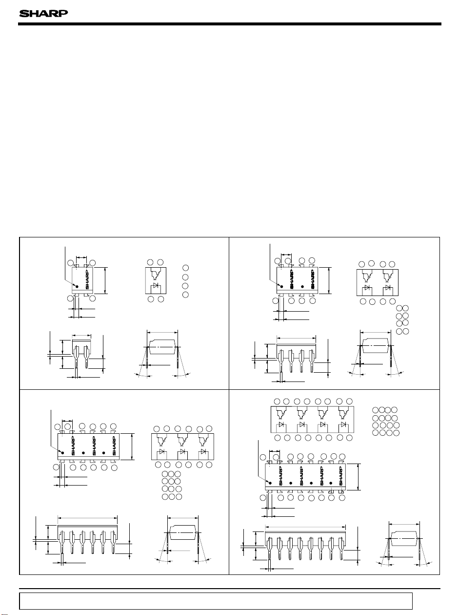
■ Outline Dimensions
PC815
TYP.
0.5
PC835
2.54
12
Anode mark
1 23456
± 0.5
TYP.
0.5
3.5
± 0.5
3.0
2.54
Anode mark
4.58
± 0.5
3.5
± 0.5
3.0
± 0.25
11
PC815
± 0.2
0.9
± 0.3
1.2
14.74
± 0.1
0.5
± 0.25
34
PC815
21
0.9
1.2
± 0.5
± 0.1
0.5
10
987
PC815
± 0.5
± 0.2
± 0.3
Internal connection diagram
± 0.5
6.5
± 0.5
2.7
θ = 0 to 13 ˚
± 0.5
PC815
6.5
± 0.2
2.7
43
12
7.62
0.26
θ
Internal connection
diagram
12
12 3456
θ = 0 to 13 ˚
)
1 Anode
2 Cathode
3 Emitter
4 Collector
± 0.3
± 0.1
θ
11
10
987
135 Anode
246 Cathode
11
7 9 Emitter
8 Collector
10
12
± 0.3
7.62
± 0.1
0.26
θ
θ
Mounting Type Photocoupler
1. System appliances, measuring instruments
2. Industrial robots
3. Copiers, automatic vending machines
4. Signal transmission between circuits of
different potentials and impedances
PC825
TYP.
PC845
± 0.5
TYP.
0.5
± 0.5
0.5
Anode mark
3.5
3.0
± 0.25
2.54
87 65
Anode mark
PC815
PC815
1 234
± 0.2
0.9
± 0.3
1.2
± 0.5
9.66
± 0.5
3.5
± 0.5
3.0
2.54
1
± 0.1
0.5
Internal connection diagram
12 345678
± 0.25
PC815
± 0.5
111213
PC815
14
1516
PC815
2345678
± 0.2
0.9
± 0.3
1.2
19.82
± 0.1
0.5
± 0.5
6.5
± 0.5
2.7
111213141516
10
10
9
PC815
θ = 0 to 13 ˚
PC815 Serise
Internal connection
diagram
87 65
12 34
± 0.3
7.62
± 0.1
0.26
θ
9
1357 Anode
2468 Cathode
11
9 Emitter
10
12
± 0.5
6.5
± 0.5
2.7
(
Unit : mm
1 3 Anode
2 4 Cathode
5 7 Emitter
6 8 Collector
θ
15
13
14
16
Collector
± 0.3
7.62
± 0.1
0.26
θ
θ = 0 to 13 ˚
)
θ
“ In the absence of confirmation by device specification sheets, SHARP takes no responsibility for any defects that occur in equipment using any of SHARP's devices, shown in catalogs,
data books, etc. Contact SHARP in order to obtain the latest version of the device specification sheets before using any SHARP's device.”
PC815 Series
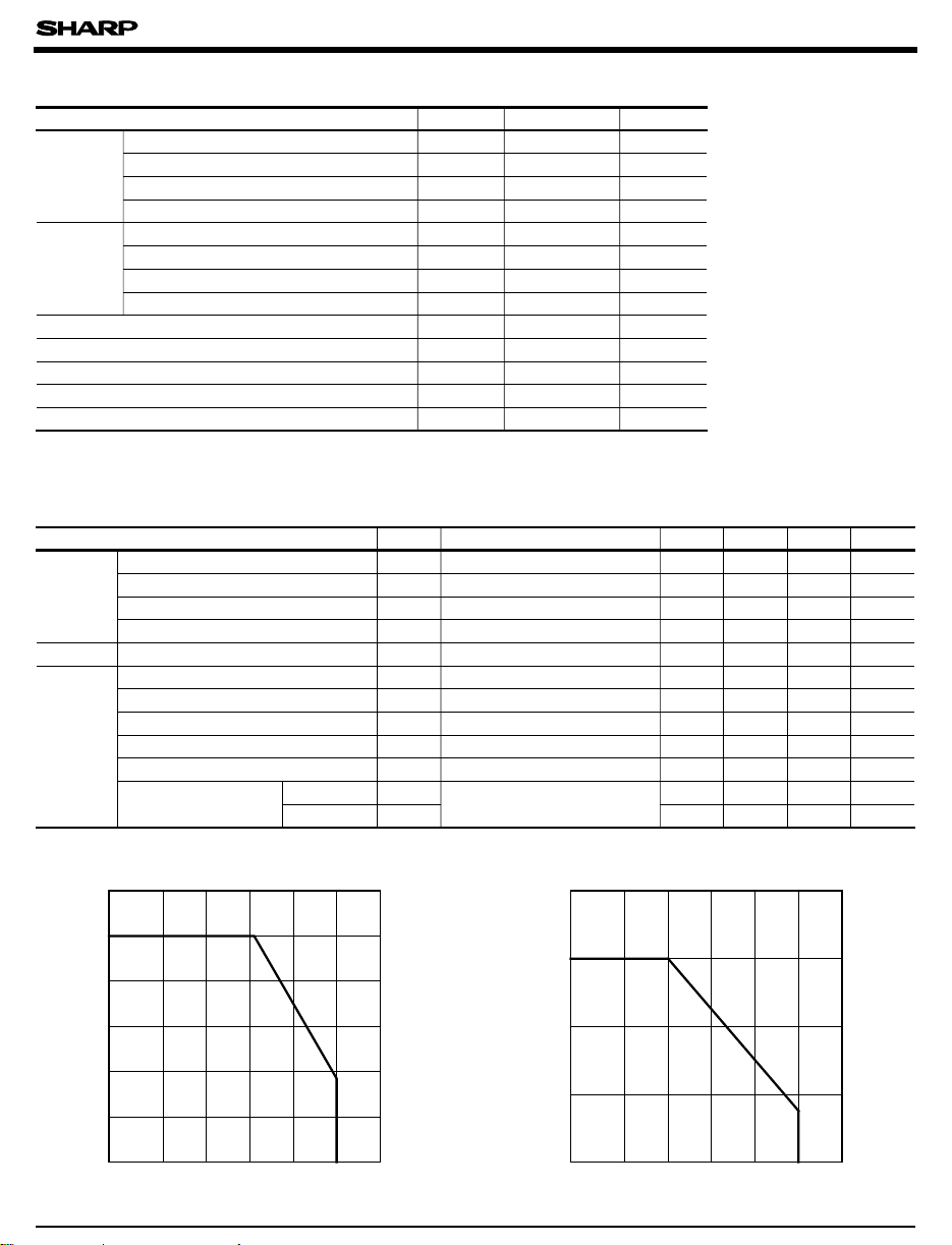
■ Absolute Maximum Ratings
Parameter Symbol Rating Unit
Forward current I
*1
Input
Peak forward current I
Reverse voltage V
Power dissipation P 70 mW
Collector-emitter voltage V
Output
Emitter-collector voltage V
Collector current I
Collector power dissipation P
Total power dissipation P
*2
Isolation voltage V
Operating temperature T
Storage temperature T
*3
Soldering temperature T
*1 Pulse width<=100µs, Duty ratio : 0.001
*2 40 to 60%RH, AC for 1 minute
*3 For 10 seconds
■ Electro-optical Characteristics
Parameter Symbol MIN. TYP. MAX. Unit
Forward voltage
Input
Output I
Transfer
charac-
teristics
Peak forward voltage
Reverse current
Terminal capacitance
Collector dark current
Current transfer ratio
Collector-emitter saturation voltage
Isolation resistance R
Floating capacitance C
Cut-off frequency f
Response time
Rise time t
Fall time t
F
FM
R
CEO
ECO
C
C
tot
iso
- 30 to + 100 ˚C
opr
- 55 to + 125 ˚C
stg
sol
(
Ta= 25˚C
50 mA
1A
6V
35 V
6V
80 mA
150 mW
200 mW
5 000
260 ˚C
)
V
rms
(
Ta= 25˚C
Conditions
V
V
C
CEO
CTR 600 %
V
CE(sat
= 20mA
I
F
F
= 0.5A
I
FM
FM
I
R
ISO
c
r
f
=4V
V
R
V= 0, f= 1kHz
t
= 10V, IF=0
V
CE
= 1mA, VCE=2V
I
F
)
= 20mA, IC= 5mA
I
F
DC500V, 40 to 60%RH
V= 0, f= 1MHz
f
VCE= 2V, IC= 2mA, RL= 100Ω
= 2V, IC= 10mA, RL= 100Ω
V
CE
- 1.2 1.4 V
- - 3.0 V
--10µA
- 30 250 pF
--10-6A
- 7 500
- 0.8 1.0 V
10
11
5x10
-
10
0.6 1.0 pF
- Ω
1 6 - kHz
-
60 300 µ s
- 53 250 µ s
)
Fig. 1 Forward Current vs.
Ambient Temperature
60
50
)
mA
(
40
F
30
20
Forward current I
10
0
-30
0 25 50 75 100 125
Ambient temperature Ta Ambient temperature Ta
(˚C)
Fig. 2 Collector Power Dissipation vs.
Ambient Temperature
200
)
mW
(
C
150
100
50
Collector power dissipation P
0
-30
0 125
25 50 75 100
(˚C)
 Loading...