


Sharp PC3H710NIP, PC3H711NIP, PC3H712NIP, PC3H715NIP, PC3Q710NIP Datasheet
...
PC3H71X NIP Series/PC3Q71X NIP Series
PC3H71X NIP Series
PC3Q71X NIP Series
■ Features
1.Low input current type(IF=0.5mA)
2.High resistance to noise due to high common rejection voltage (CMR:MIN. 10kV/μs)
3.Mini-flat package
4.Isolation voltage (Viso:2.5kVrms)
5.Recognized by UL, file No. E64380
■ Applications
1.Programmable controllers
2.Facsimiles
3.Telephones
■ Rank Table
Model No. |
Rank mark |
Ic (mA) |
Conditions |
|
PC3H710NIP |
A, B or no mark |
0.5 to 3.5 |
IF=0.5mA |
|
PC3H711NIP |
A |
0.7 to 1.75 |
||
VCE=5V |
||||
PC3H712NIP |
B |
1.0 to 2.5 |
||
Ta=25°C |
||||
PC3H715NIP |
A or B |
0.7 to 2.5 |
||
|
||||
|
|
|
|
|
Model No. |
Rank mark |
Ic (mA) |
Conditions |
|
PC3Q710NIP |
A or no mark |
0.5 to 3.0 |
IF=0.5mA |
|
VCE=5V |
||||
PC3Q711NIP |
|
|
||
A |
1.0 to 2.5 |
Ta=25°C |
■ Absolute Maximum Ratings |
(Ta=25°C) |
|||||
|
Parameter |
Symbol |
Rating |
|
Unit |
|
|
Forward current |
IF |
10 |
|
mA |
|
Input |
*1 Peak forward current |
IFM |
200 |
|
mA |
|
Reverse voltage |
VR |
6 |
|
V |
|
|
|
|
|||||
|
Power dissipation |
P |
15 |
|
mW |
|
|
Collector-emitter voltage |
VCEO |
70 |
|
V |
|
Output |
Emitter-collector voltage |
VECO |
6 |
|
V |
|
Collector current |
IC |
50 |
|
mA |
||
|
|
|||||
|
|
|
|
|
|
|
|
Collector power dissipation |
PC |
150 |
|
mW |
|
|
Total power dissipation |
Ptot |
170 |
|
mW |
|
|
Operating temperature |
Topr |
−30 to +100 |
°C |
|
|
|
Storage temperature |
Tstg |
−40 to +125 |
°C |
|
|
|
*2 Isolation voltage |
Viso |
2.5 |
|
kVrms |
|
|
*3 Soldering temperature |
Tsol |
260 |
|
°C |
|
*1 Pulse width<=100μs, Duty ratio=0.001 *2 40 to 60%RH, AC for 1 minute, f=60Hz *3 For 10s
Low Input Current Type
Photocoupler
■ Outline Dimensions |
(Unit : mm) |
PC3H71xNIP Series |
|
|
|
|
|
Internal connection |
||||||||||
|
|
|
|
|
|
|
|
|
||||||||
|
Anode mark |
|
|
|
|
|
diagram |
|
|
|
|
|||||
|
|
|
|
|
|
4 |
|
3 |
|
|
|
|
|
|||
|
|
|
1 |
|
|
|
4 |
|
|
|
|
|
|
|
||
±0.3 |
±0.25 |
|
|
|
|
|
|
|
|
|
|
|
|
|
||
|
|
|
|
|
|
|
|
|
|
|
1 |
Anode |
||||
|
|
|
|
|
|
|
|
|
|
|
|
Cathode |
||||
2.6 |
1.27 |
H 7 1 |
|
|
|
|
|
|
|
2 |
||||||
|
|
|
|
|
|
|
3 |
Emitter |
||||||||
2 |
|
|
|
3 |
±0.1 |
|
|
|
|
|||||||
|
|
|
4.4±0.2 |
|
|
|
|
|
|
4 |
Collector |
|||||
|
|
|
|
|
|
|
|
0.4 |
1 |
|
2 |
|
|
|
|
|
|
|
|
|
|
|
|
|
|
|
|
|
|
|
|
||
|
|
|
5.3±0.3 |
|
|
|
|
|
|
Epoxy resin |
||||||
|
|
±0.05 |
|
|
|
|
±0.2 |
|
|
|
|
|
|
|
|
|
|
|
|
0.2 |
|
0.5+0.4 |
2.0 |
|
|
|
|
|
|
|
|
||
|
|
|
|
|
0.1 |
|
|
|
|
|
|
|
|
|||
|
|
|
7.0−+0.70.2 |
|
|
−0.2 |
± |
|
|
|
|
|
|
|
|
|
|
|
|
|
|
|
|
0.1 |
|
|
|
|
|
|
|
|
|
PC3Q71xNIP Series |
|
|
|
|
|
|
|
|
|
|
|
|
|
|||
|
|
|
10.3±0.3 |
|
|
|
|
|
Internal connection |
|||||||
|
|
|
1.27±0.25 |
|
|
|
|
|
diagram |
|
|
|
|
|||
|
|
|
|
|
|
|
|
16 |
15 14 |
13 12 |
11 10 |
9 |
||||
|
16 |
|
|
9 |
|
|
|
|||||||||
|
|
|
|
|
|
|
|
|
|
|
|
|
|
|||
|
|
|
P C 3 Q 7 1 |
|
|
±0.2 |
|
|
|
|
|
|
|
|
|
|
|
|
|
|
|
4.4 |
|
|
1 |
2 |
3 |
4 |
5 |
6 |
7 |
8 |
|
|
|
|
|
|
|
|
|
|||||||||
|
|
|
|
|
|
|
|
|
|
|
|
|
|
|
|
|
|
|
|
|
|
|
|
|
|
1 |
3 |
5 |
7 |
Anode |
|
||
|
|
|
|
|
|
|
±0.1 |
|
2 |
4 |
6 |
8 |
Cathode |
|||
|
1 |
|
|
8 |
0.4 |
|
9 |
11 |
13 |
15 |
Emitter |
|
||||
|
|
|
|
|
10 |
12 |
14 |
16 |
Collector |
|||||||
|
|
|
Primary side mark |
|
|
|
||||||||||
|
|
|
|
|
|
|
|
|
|
|
|
|
|
|||
±0.2 |
|
|
|
|
|
|
C0.4 |
|
|
|
|
|
|
|
|
|
|
Epoxy resin |
|
|
|
(Input side) |
|
5.3±0.3 |
|
|
|
||||||
|
2.6 |
|
|
|
|
|
|
|
|
|
|
|||||
|
|
|
|
|
|
|
0.05 |
|
|
|
|
|
||||
|
|
|
|
|
|
|
|
|
|
|
|
|
|
|
||
|
|
|
|
|
|
|
|
± |
|
|
|
|
|
|
|
|
|
|
|
|
|
|
|
|
0.2 |
|
|
|
|
|
|
|
|
|
|
|
|
|
|
|
|
|
|
|
|
0.5+0.4 |
|
|
||
±0.1 |
|
|
6 |
° |
|
|
|
|
|
|
|
−0.2 |
|
|
||
|
|
|
|
|
|
|
7.0−+0.70.2 |
|
|
|
||||||
|
0.1 |
|
|
|
|
|
|
|
|
|
|
|
|
|||
 0.2mm or more
Soldering area
Notice |
In the absence of confirmation by device specification sheets, SHARP takes no responsibility for any defects that may occur in equipment using any SHARP |
|
devices shown in catalogs, data books, etc. Contact SHARP in order to obtain the latest device specification sheets before using any SHARP device. |
Internet |
Internet address for Electronic Components Group http://www.sharp.co.jp/ecg/ |
PC3H71X NIP Series/PC3Q71X NIP Series
■ Electro-optical Characteristics |
|
|
|
(Ta=25°C) |
||||||
|
Parameter |
Symbol |
Conditions |
MIN. |
TYP. |
MAX. |
Unit |
|
||
Input |
Forward voltage |
VF |
IF=10mA |
− |
1.2 |
1.4 |
V |
|||
|
Reverse current |
IR |
VR=4V |
− |
− |
10 |
μA |
|
||
|
Terminal capacitance |
Ct |
V=0, f=1kHz |
− |
30 |
250 |
pF |
|
||
Output |
Collector dark current |
ICEO |
VCE=50V, IF=0 |
− |
− |
100 |
nA |
|
||
Collector-emitter breakdown voltage |
BVCEO |
IC=0.1mA, IF=0 |
70 |
− |
− |
V |
|
|||
|
||||||||||
|
Emitter-collector breakdown voltage |
BVECO |
IE=10μA, IF=0 |
6 |
− |
− |
V |
|
||
|
Collector |
PC3H71XNIP Series |
IC |
IF=0.5mA, VCE=5V |
0.5 |
− |
3.5 |
mA |
||
characteristics |
current |
PC3Q71XNIP Series |
3.0 |
|||||||
|
|
|
|
|
|
|||||
|
|
|
|
|
|
|
||||
|
Collector-emitter saturation voltage |
VCE (sat) |
IF=10mA, IC=1mA |
− |
− |
0.2 |
V |
|||
|
Isolation resistance |
RISO |
DC500V 40 to 60%RH |
5×10¹⁰ |
1×10¹¹ |
− |
Ω |
|
||
|
Floating capacitance |
Cf |
V=0, f=1MHz |
− |
0.6 |
1.0 |
pF |
|||
Transfer |
|
Rise time |
tr |
|
− |
4 |
18 |
μs |
|
|
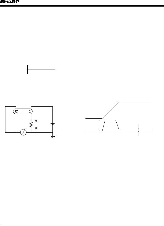
*1 Common mode rejection voltage |
CMR |
Ta=25°C, RL=470Ω, VCM=1.5kV (peak), |
10 |
− |
− |
kV/μs |
|
|||
|
Response time |
tf |
VCE=2V, IC=2mA, RL=100Ω |
− |
3 |
18 |
μs |
|||
|
|
Fall time |
|
|||||||
|
|
|
|
IF=0mA, VCC=9V, Vnp=100mV |
|
|
|
|
|
|
|
|
|
|
|
|
|
|
|
|
|
*1 Refer to Fig.1. |
|
|
|
|
|
|
|
|
||
Fig.1 Test Circuit for Common Mode Rejection Voltage
|
|
|
(dV/dt) |
|
|
|
|
VCM |
|
RL |
VCC |
1) |
Vnp |
|
Vnp |
|
Vcp |
||
|
é |
VCM : High wave |
VO |
|
|
ê |
pulse |
(Vcp Nearly = dV/dt´Cf´RL) |
|
VCM |
ê |
|
||
ê RL=470W |
1) Vcp : Voltage which is generated by displacement current in floating |
|||
|
ë VCC=9V |
capacitance between primary and secondary side. |
||
Fig.2 Forward Current vs. Ambient Temperature
(mA) |
10 |
|
|
|
|
|
|
|
|
|
|
|
|
F |
|
|
|
|
|
|
|
|
|
|
|
|
|
|
|
|
|
|
|
|
|
|
|
|
|
|
|
current I |
|
|
|
|
|
|
|
|
|
|
|
|
|
Forward |
5 |
|
|
|
|
|
|
|
|
|
|
|
|
|
|
|
|
|
|
|
|
|
|
|
|
|
|
|
0 |
|
|
|
|
|
|
|
|
|
|
|
|
|
-30 |
0 |
25 |
50 |
75 |
100 |
125 |
||||||
Ambient temperature Ta (°C)
Fig.3 Diode Power Dissipation vs. Ambient Temperature
P (mW) |
15 |
|
|
|
|
|
|
|
|
|
|
|
|
|
|
|
|
|
|
|
|
|
|
|
|
||
|
|
|
|
|
|
|
|
|
|
|
|
|
|
power dissipation |
10 |
|
|
|
|
|
|
|
|
|
|
|
|
Diode |
5 |
|
|
|
|
|
|
|
|
|
|
|
|
|
|
|
|
|
|
|
|
|
|
|
|
|
|
|
0 |
|
|
|
|
|
|
|
|
|
|
|
|
|
-30 |
0 |
25 |
50 |
75 |
100 |
125 |
||||||
Ambient temperature Ta (°C)
 Loading...