


PC812
PC812
■Features
1.High noise reduction
( Common mode rejection voltage
V CM : TYP. 1.5kV at dV/dt = 2kV/ μ s, R L = 470 Ω , V np = 100mV )
2.High current transfer ratio
( CTR : MIN. 90% at I F = 5mA, V CE = 5V)
3.High isolation voltage between input and output ( Viso : 5 000V rms )
4.Compact dual-in-line package
■Applications
1.Motor-control circuits
2.Computer terminals
3.System appliances, measuring instruments
4.Signal transmission between circuits of different potentials and impedances
High Noise Resistance Type
Photocoupler
■ Outline Dimensions |
|
( Unit : mm) |
|||||
|
|
|
|
|
Internal connection |
||
|
mark |
|
2.54± |
0.25 |
diagram |
|
|
|
4 |
4 |
3 |
|
|||
|
rank |
|
3 |
|
|
|
|
|
|
PC812 |
± 0.5 |
|
|
|
|
Anode mark |
CTR |
|
|
|
|
||
1 |
6.5 |
1 |
2 |
|
|||
|
|
|
2 |
Anode |
3 |
Emitter |
|
|
0.9 ± 0.2 |
|
1 |
||||
|
|
2 |
Cathode |
4 |
Collector |
||
|
1.2 ± 0.3 |
|
|||||
|
|
|
|
|
|
||
|
|
|
4.58 ± 0.5 |
7.62 ± 0.3 |
|
||
|
0.5TYP. |
± 0.5 |
|
|
|
|
|
|
3.5 |
|
|
|
|
|
|
|
|
± 0.5 |
|
|
|
|
|
|
|
3.0 |
|
|
θ |
|
θ |
|
|
|
|
0.5 ± 0.1 |
|
||
|
|
|
|
|
θ = 0 to 13 ˚ |
0.26 ± 0.1 |
|
|
|
|
|
|
|
||
■ Absolute Maximum Ratings |
|
(Ta= 25˚C) |
|
|
|
|
|
Parameter |
Symbol |
Rating |
Unit |
Forward current |
IF |
50 |
mA |
*1Peak forward current |
I FM |
1 |
A |
Input |
V R |
6 |
V |
Reverse voltage |
|||
Power dissipation |
P |
70 |
mW |
Collector-emitter voltage |
V CEO |
35 |
V |
Emitter-collector voltage |
V ECO |
6 |
V |
Output |
IC |
50 |
mA |
Collector current |
|||
Collector power dissipation |
P C |
150 |
mW |
Total power dissipation |
P tot |
200 |
mW |
*2Isolation voltage |
V iso |
5 000 |
V rms |
Operating temperature |
T opr |
- 30 to + 100 |
˚C |
Storage temperature |
T stg |
- 55 to + 125 |
˚C |
*3Soldering temperature |
T sol |
260 |
˚C |
*1 Pulse width <=100 μ s, Duty ratio : 0.001 *2 40 to 60% RH, AC for 1 minute
*3 For 10 seconds
“In the absence of confirmation by device specification sheets, SHARP takes no responsibility for any defects that occur in equipment using any of SHARP's devices, shown in catalogs, data books, etc. Contact SHARP in order to obtain the latest version of the device specification sheets before using any SHARP's device.”
|
|
|
|
|
|
|
|
|
PC812 |
|
|
■ Electro-optical Characteristics |
|
|
|
|
(Ta = 25˚C) |
||||||
|
|
|
|
|
|
|
|
|
|
|
|
|
|
Parameter |
Symbol |
Conditions |
MIN. |
T Y P . |
M A X . |
Unit |
|
||
|
|
Forward voltage |
V F |
IF = 20mA |
- |
1.2 |
1.4 |
|
V |
||
Input |
|
Peak forward voltage |
V F M |
IF M = 0.5A |
- |
- |
3.0 |
|
V |
|
|
|
Reverse current |
IR |
V R = 4V |
- |
- |
10 |
|
μ A |
|
||
|
|
|
|||||||||
|
|
Terminal capacitance |
Ct |
V = 0, f = 1kHz |
- |
30 |
200 |
|
p F |
|
|
Output |
|
Collector dark current |
ICEO |
V CE = 20V, IF = 0 |
- |
- |
10 - 7 |
|
A |
||
|
*4 Current transfer ratio |
C T R |
IF = 5 mA, VCE = 5V |
90 |
- |
480 |
|
% |
|
||
|
|
Collector-emitter saturation voltage |
V CE ( sat ) |
IF = 20mA, IC = 1mA |
- |
0.1 |
0.2 |
|
V |
||
Transfer |
|
Isolation resistance |
R ISO |
DC500V, 40 to 60% RH |
5 x 10¹⁰ |
1011 |
- |
|
Ω |
|
|
|
Floating capacitance |
Cf |
V = 0, f = 1MHz |
- |
0.6 |
1.0 |
|
p F |
|
||
charac- |
|
|
|||||||||
|
Cut-off frequency |
fc |
VCE = 5V, IC = 2mA, RL = 100 Ω, - 3dB |
15 |
80 |
- |
|
k H z |
|
||
teristics |
|
|
|||||||||
|
*4 |
Response time |
Rise time |
t r |
VCE = 2V, IC = 2mA, RL = 100 Ω |
- |
4 |
18 |
|
μ s |
|
|
Fall time |
tf |
- |
5 |
20 |
|
μ s |
|
|||
|
|
|
|
|
|||||||
|
*5 Common mode rejection voltage |
V CM |
dV/dt = 2kV/ μ s, RL = 470 Ω, Vnp = 100mV, IF = 0 |
- |
1.5 |
- |
|
k V |
|
||
*4 Classification table of current transfer ratio is shown below.
Model |
Rank |
CTR ( % ) |
t r ( μ s) |
tf ( μ s) |
|||
No. |
mark |
T Y P . M A X . T Y P . M A X . |
|||||
|
|||||||
PC812A |
A |
90 to 180 |
3 |
14 |
4 |
16 |
|
PC812B |
B |
150 to 180 |
4 |
16 |
5 |
18 |
|
PC812C |
C |
240 to 480 |
5 |
18 |
7 |
20 |
|
PC812 |
A , B o r C |
90 to 480 |
4 |
18 |
5 |
20 |
|
|
|
|
|
V CE = 2V |
|
||
Measurement |
I = 5mA |
|
IC = 2mA |
|
|||
conditions |
VCE = 5V |
|
R L = 100 Ω |
|
|||
|
|
Ta = 25˚C |
|
Ta = 25˚C |
|
||
|
|
|
|
|
|||
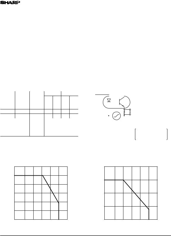
*5 Test Circuit for VCM
|
|
|
|
|
RL |
|
|
|
|
|
|
VCC = 9V |
|
|
|
|
|
|
|
|
|
|
|
||
|
|
|
|
|
|
|
|
|
|
|
||
|
|
|
|
|
|
Vnp |
|
|
|
|||
|
|
|
|
|
|
|
|
|
||||
|
|
|
|
|
|
|
|
|
|
|||
|
|
|
VCM |
|
|
|
|
|
|
|
||
VCM : Common mode rejection |
|
Test condition |
||||||||||
voltage |
|
Vnp = 100mV, RL = 470 Ω |
||||||||||
(higher value of pulse wave) |
|
dV/dt = 2kV/ μ s, IF = 0 |
||||||||||
dV/dt : Rising factor of voltage |
|
|
|
|
|
|
|
|||||
Fig. 1 Forward Current vs.
Ambient Temperature
|
60 |
|
|
|
|
|
|
|
50 |
|
|
|
|
|
|
) |
|
|
|
|
|
|
|
mA |
40 |
|
|
|
|
|
|
|
|
|
|
|
|
|
|
( |
|
|
|
|
|
|
|
F |
|
|
|
|
|
|
|
I |
30 |
|
|
|
|
|
|
current |
|
|
|
|
|
|
|
20 |
|
|
|
|
|
|
|
Forward |
|
|
|
|
|
|
|
10 |
|
|
|
|
|
|
|
|
|
|
|
|
|
|
|
|
0 |
|
|
|
|
|
|
|
- 30 |
0 |
25 |
50 |
75 |
100 |
125 |
|
|
Ambient temperature T a (˚C) |
|
|
|||
Fig. 2 Collector Power Dissipation vs. Ambient Temperature
|
200 |
|
|
|
|
|
|
) |
|
|
|
|
|
|
|
mW |
|
|
|
|
|
|
|
( |
|
|
|
|
|
|
|
C |
150 |
|
|
|
|
|
|
P |
|
|
|
|
|
|
|
dissipation |
100 |
|
|
|
|
|
|
power |
|
|
|
|
|
|
|
Collector |
50 |
|
|
|
|
|
|
|
|
|
|
|
|
|
|
|
0 |
|
|
|
|
|
|
|
- 30 |
0 |
25 |
50 |
75 |
100 |
125 |
|
|
Ambient temperature T a |
( ˚C ) |
|
|||
 Loading...