


PC829 Series
PC829 Series |
High Density Mounting Type |
Photocoupler |
|
.. |
|
TUV |
( VDE0884 ) approved type is also available as an option. |
|
|
|
|
|
|
|
|
|
|
|
|
|
|
|
|
|
|||
■ Features |
|
|
■ Outline Dimensions |
|
|
|
|
|
( Unit : mm ) |
||||||||||||
1. Symmetrical terminal configuration |
|
PC829 |
|
|
|
1.2 ± 0.3 |
|
|
Internal connection |
|
|
||||||||||
PC829 : 2-channel type |
|
|
|
|
|
|
|
0.9 ± 0.2 |
|
|
diagram |
|
|
|
|
|
|||||
|
|
|
|
|
|
8 |
7 |
6 |
|
5 |
|
8 |
7 |
|
6 |
5 |
|
|
|
||
PC849 : 4-channel type |
|
|
|
|
|
|
|
|
|
|
|
|
|||||||||
|
|
|
|
|
|
PC829 |
|
0.5 |
|
|
|
|
|
|
|
|
|
||||
2. High current transfer ratio |
|
|
|
|
|
|
|
|
|
|
|
|
|
|
|
|
|||||
|
|
|
|
|
|
|
|
|
|
± |
|
|
|
|
|
|
|
|
|
||
( CTR : MIN. 50% at IF = 5mA, VCE = 5V) |
|
|
|
|
|
|
|
|
6.5 |
|
|
|
|
|
|
|
|
|
|||
|
|
|
|
1 |
2 |
3 |
|
4 |
|
1 |
2 |
|
3 |
4 |
|
|
|
||||
3. High isolation voltage between input and |
|
|
|
|
|
|
|
|
|
|
|||||||||||
|
|
|
|
|
|
|
|
|
|
|
|
|
|
||||||||
|
Anode mark |
|
|
|
2.54 ± 0.25 |
|
|
|
|
|
|
|
|
||||||||
output ( Viso : 5 000V rms ) |
|
|
|
|
|
|
|
|
|
|
|
|
|
|
|||||||
|
|
|
|
|
|
9.66 ± 0.5 |
|
|
|
|
|
|
7.62 ± 0.3 |
|
|
||||||
4. Recognized by UL, file No. E64380 |
|
|
0.5TYP. |
3.5 |
|
|
|
|
|
|
|
|
|
||||||||
|
|
|
0.5 |
|
|
|
|
|
|
|
|
|
|
|
|
|
|
|
|||
|
|
|
|
|
|
± |
|
|
|
|
|
|
|
|
|
|
|
|
|
|
|
■ Applications |
|
|
|
|
± 0.5 |
|
|
|
|
|
|
|
|
|
|
0.26 ± 0.1 |
|
|
|||
|
|
|
|
3.0 |
|
|
|
|
|
0.5 ± 0.1 |
|
|
|
θ |
|
|
|
θ |
|
||
1. Telephone exchangers |
|
|
|
|
|
|
|
|
|
|
|
|
|
|
|
|
|||||
|
|
1 |
4 |
Anode |
|
5 |
8 |
Emitter |
|
|
θ = 0 to 13 ˚ |
|
|
||||||||
2. Computer terminals |
|
|
|
|
|
|
|
||||||||||||||
|
|
2 |
3 |
Cathode |
|
6 |
7 |
Collector |
|
|
|
|
|
|
|
|
|||||
3. System appliances, measuring instruments |
PC849 |
|
|
|
1.2 ± 0.3 |
|
|
Internal connection |
|
|
|||||||||||
4. Signal transmission between circuits of |
|
|
|
|
|
0.9 ± 0.2 |
|
|
diagram |
|
|
|
|
|
|||||||
16 |
15 |
14 |
13 |
12 |
11 |
10 |
|
9 |
16 |
15 |
|
14 |
13 |
12 |
11 |
10 |
9 |
||||
different potentials and impedances |
|
|
|
|
|
|
|
|
|
|
|
||||||||||
|
|
|
|
PC849 |
|
|
0.5 |
|
|
|
|
|
|
|
|
|
|||||
|
|
|
|
|
|
|
|
|
|
|
|
± |
|
|
|
|
|
|
|
|
|
|
|
|
|
|
|
|
|
|
|
|
|
6.5 |
|
|
|
|
|
|
|
|
|
|
|
|
|
1 |
2 |
3 |
4 |
5 |
6 |
7 |
8 |
1 |
2 |
|
3 |
4 |
5 |
6 |
7 |
8 |
|
|
|
|
|
|
|
|
|
|
|
|
|
|
|||||||||
|
|
|
|
Anode mark |
|
|
|
|
2.54 ± 0.25 |
|
|
|
|
|
|
|
|
||||
|
|
|
|
|
|
|
19.82 ± 0.5 |
|
|
3.5 |
0.5TYP. |
|
|
|
7.62 ± 0.3 |
|
|
||||
|
|
|
|
|
|
|
|
|
|
|
|
± 0.5 |
|
|
|
|
|
|
|
|
|
|
|
|
|
|
|
|
|
|
|
|
|
|
0.5 |
|
|
|
0.26 ± 0.1 |
|
|
||
|
|
|
|
|
|
|
|
|
|
|
|
|
± |
|
|
θ |
|
|
|
θ |
|
|
|
|
|
|
|
|
|
|
0.5 ± 0.1 |
|
3.0 |
|
|
|
|
|
|
||||
■ Absolute Maximum Ratings |
(Ta = 25˚C ) |
|
|
|
|
|
|
|
|
|
|
|
θ = 0 to 13 ˚ |
|
|
||||||
1 |
4 |
5 |
8 |
Anode |
|
9 12 13 16 |
|
|
Emitter |
|
|
|
|||||||||
|
Parameter |
Symbol |
Rating |
Unit |
|
|
|
|
|
|
|||||||||||
|
2 |
3 |
6 |
7 |
Cathode |
10 11 14 15 |
|
Collector |
|
|
|||||||||||
|
Forward current |
IF |
50 |
mA |
|
|
|
|
|
|
|
|
|
|
|
|
|
|
|
|
|
Input |
*1Peak forward current |
IFM |
1 |
A |
|
|
|
|
|
|
|
|
|
|
|
|
|
|
|
|
|
Reverse voltage |
VR |
6 |
V |
|
|
|
|
|
|
|
|
|
|
|
|
|
|
|
|
|
|
|
|
|
|
|
|
|
|
|
|
|
|
|
|
|
|
|
|
||||
|
Power dissipation |
P |
70 |
mW |
|
|
|
|
|
|
|
|
|
|
|
|
|
|
|
|
|
|
Collector-emitter voltage |
V CEO |
35 |
V |
|
|
|
|
|
|
|
|
|
|
|
|
|
|
|
|
|
Output |
Emitter-collector voltage |
V ECO |
6 |
V |
|
|
|
|
|
|
|
|
|
|
|
|
|
|
|
|
|
Collector current |
IC |
50 |
mA |
|
|
|
|
|
|
|
|
|
|
|
|
|
|
|
|
|
|
|
|
|
|
|
|
|
|
|
|
|
|
|
|
|
|
|
|
||||
|
Collector power dissipation |
PC |
150 |
mW |
|
|
|
|
|
|
|
|
|
|
|
|
|
|
|
|
|
|
Total power dissipation |
P tot |
170 |
mW |
|
*2Isolation voltage |
V iso |
5 000 |
V rms |
|
Operating temperature |
T opr |
- 25 to + 100 |
˚C |
|
Storage temperature |
T stg |
- 40 to + 125 |
˚C |
|
*3Soldering temperature |
T sol |
260 |
˚C |
*1 |
Pulse width<=100μs, Duty ratio : 0.001 |
|
|
|
*2 |
40 to 60% RH, AC for 1 minute |
|
|
|
*3 |
For 10 seconds |
|
|
|
“ In the absence of confirmation by device specification sheets, SHARP takes no responsibility for any defects that occur in equipment using any of SHARP's devices, shown in catalogs, data books, etc. Contact SHARP in order to obtain the latest version of the device specification sheets before using any SHARP's device.”
PC829 Series
■ Electro-optical Characteristics |
|
|
|
|
( Ta = 25˚C) |
||||
|
|
|
|
|
|
|
|
|
|
|
Parameter |
Symbol |
Conditions |
MIN. |
TYP. |
MAX. |
Unit |
||
|
Forward voltage |
V F |
IF = 20mA |
- |
1.2 |
1.4 |
V |
||
Input |
Peak forward voltage |
V FM |
IFM = 0.5A |
- |
- |
3.0 |
V |
||
Reverse current |
IR |
V R = 4V |
- |
- |
10 |
μ A |
|||
|
|||||||||
|
Terminal capacitance |
Ct |
V = 0, f = 1kHz |
- |
30 |
250 |
pF |
||
Output |
Collector dark current |
ICEO |
V CE = 20V, I F = 0 |
- |
- |
10 - 7 |
A |
||
|
Current transfer ratio |
CTR |
IF = 5mA, V CE = 5V |
50 |
- |
400 |
% |
||
|
Collector-emitter saturation voltage |
V CE( sat ) |
IF = 20mA, I C = 1mA |
- |
0.1 |
0.2 |
V |
||
Transfer |
Isolation resistance |
R ISO |
DC500V, 40 to 60% RH |
5 x 10¹⁰ |
1011 |
- |
Ω |
||
charac- |
Floating capacitance |
Cf |
V = 0, f = 1MHz |
- |
0.6 |
1.0 |
pF |
||
teristics |
Cut-off frequency |
fc |
VCE = 5V, I C = 2mA, R L = 100 Ω, - 3dB |
- |
80 |
- |
kHz |
||
|
Response time |
Rise time |
t r |
VCE = 2V, I C = 2mA, R L = 100 Ω |
- |
4 |
- |
μ s |
|
|
Fall time |
tf |
- |
3 |
- |
μ s |
|||
|
|
|
|||||||
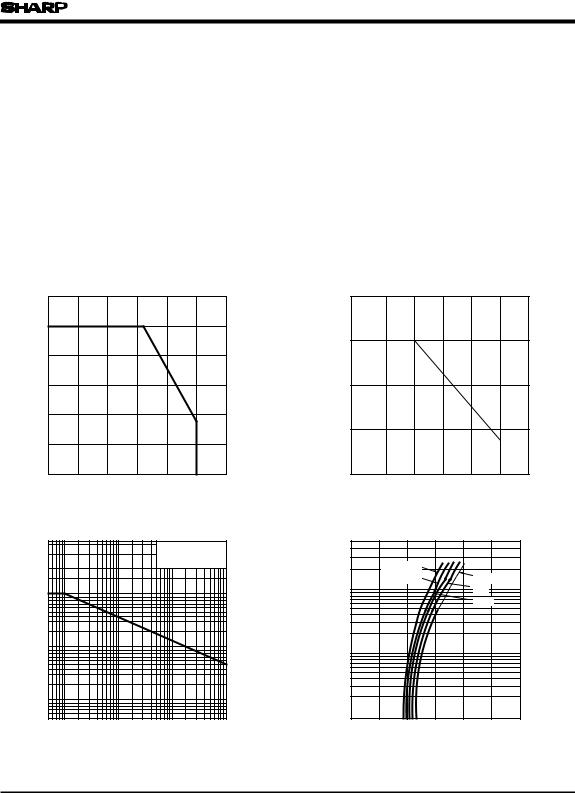
Fig. 1 Forward Current vs.
Ambient Temperature
|
60 |
|
|
|
|
|
|
|
50 |
|
|
|
|
|
|
) |
|
|
|
|
|
|
|
mA |
40 |
|
|
|
|
|
|
( |
|
|
|
|
|
|
|
F |
|
|
|
|
|
|
|
I |
|
|
|
|
|
|
|
current |
30 |
|
|
|
|
|
|
|
|
|
|
|
|
|
|
Forward |
20 |
|
|
|
|
|
|
|
|
|
|
|
|
|
|
|
10 |
|
|
|
|
|
|
|
0 |
|
|
|
|
|
|
|
- 25 |
0 |
25 |
50 |
75 |
100 |
125 |
|
|
|
Ambient temperature T a (˚C) |
|
|
||
Fig. 3 Peak Forward Current vs. Duty Ratio
10 000
 Pulse width <=100 μs 5 000
  Ta = 25˚C
) |
2 000 |
mA |
1 000 |
( |
|
FM |
500 |
I |
|
current |
200 |
|
|
Peakforward |
100 |
20 |
|
|
50 |
10
5
5 10 - 3 2 |
5 10 - 2 2 |
5 10 - 1 2 |
5 |
1 |
Duty ratio
Fig. 2 Collector Power Dissipation vs. Ambient Temperature
|
200 |
|
|
|
|
|
|
) |
|
|
|
|
|
|
|
mW |
|
|
|
|
|
|
|
( |
150 |
|
|
|
|
|
|
C |
|
|
|
|
|
|
|
|
|
|
|
|
|
|
|
P |
|
|
|
|
|
|
|
power dissipation |
100 |
|
|
|
|
|
|
|
|
|
|
|
|
|
|
Collector |
50 |
|
|
|
|
|
|
|
|
|
|
|
|
|
|
|
0 |
|
|
|
|
|
|
|
- 25 |
0 |
25 |
50 |
75 |
100 |
125 |
|
|
|
Ambient temperature T a ( ˚C ) |
|
|||
Fig. 4 Forward Current vs. Forward Voltage
|
500 |
|
|
|
|
|
|
|
200 |
Ta = 75˚C |
|
|
- 25˚C |
|
|
|
|
|
50˚C |
|
|
|
|
) |
100 |
|
|
|
|
0˚C |
|
mA |
|
|
|
|
|
||
|
|
|
|
|
25˚C |
|
|
( |
50 |
|
|
|
|
|
|
F |
|
|
|
|
|
|
|
I |
|
|
|
|
|
|
|
current |
20 |
|
|
|
|
|
|
|
|
|
|
|
|
|
|
Forward |
10 |
|
|
|
|
|
|
5 |
|
|
|
|
|
|
|
|
2 |
|
|
|
|
|
|
|
1 |
|
|
|
|
|
|
|
0 |
0.5 |
1.0 |
1.5 |
2.0 |
2.5 |
3.0 |
|
|
|
Forward voltage V F (V) |
|
|||
 Loading...