


LC-26SD1E/RU, LC-32SD1E/RU
CHAPTER 7. MAJOR IC INFORMATIONS
[1] MAJOR IC INFORMATIONS
1. General ICs Information
Ref No. |
Name |
Part Code |
Description |
|
KD890FM (MAIN UNIT) |
|
|
||
IC1905 |
1 |
HDMI-Receiver |
VHISII9021+-1Q |
The SiI9021 is a second generation panel Link Cinema receiver that is compatible with the |
|
|
|
|
HDMI 1.1 (High Definition Multimedia interface) specification. |
|
|
|
|
The SiI9021 is capable of receiving and outputting two channel digital audio at up to 192KHz |
|
|
|
|
- an excellent solution for Digital TVs. |
|
|
|
|
The feature of this IC is as follows. |
|
|
|
|
1) Digital video interface supports video processors: |
|
|
|
|
2) Analog RGB and YPbPr output: 10-bit DAC. |
|
|
|
|
3) Digital audio interface supports high-end audio systems: |
IC2701 |
2 |
4CH- |
VHITVHC153T-1Y |
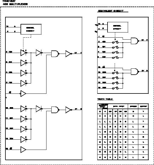
This IC is a super high speed CMOS 4-channel multiplexer using the CMOS technology and |
|
|
MULTIPLEXER |
|
incorporates 2 circuits. |
|
|
|
|
The input consists of 2 addresses A, B, 4 channel inputs C0-C3 and strobe input G, and the |
|
|
|
|
signal of the channel selected by the address input sent as the output Y. |
|
|
|
|
The strobe input is used for prohibition of data output. |
|
|
|
|
That means, when G input is “H” the output becomes “L” unconditionally. |
|
|
|
|
In this model, this IC operates the switch of H/V-SYNC on each signal condition. |
IC3002 |
3 |
VIDEO |
RH-IXB624WJN1Q |
The VCT 6wxyP family is based on functional blocks contained and approved in existing |
|
|
PROCESSOR |
|
products like VCT49xxl, VSP 94x5B, and DPS 94xxA. |
|
|
|
|
That is, the following 6 major functions are included: |
|
|
|
|
1) Audio Processing |
|
|
|
|
2) Video Processing |
|
|
|
|
3) Motion Adaptive Upconversion |
|
|
|
|
4) Scaling, Display Processing and FPD |
|
|
|
|
5) Unified memory for Audio, Video and Text Control, 3D Combfilter PC |
|
|
|
|
Connectivity |
|
|
|
|
6) Controlling, OSD and Text |
IC3003 |
3 |
Microcontroller |
RH-IXB664WJZZY |
This IC is based on LCD Driver and nano Watt Technology and is RISC microprocessor to |
|
|
|
|
control peripheral functions necessary for the system configuration. |
|
|
|
|
In this equipment, the R/C LED on the AVC side and system on the display side are con- |
|
|
|
|
trolled. |
IC2301 |
5 |
RS232C |
VHIISL83220-1Y |
This IC is a line driver receiver in conformity with EIA/TIA-232-E (former RS-232C) standard. |
|
|
Transmitters/ |
|
By connecting a PC, the system can be controlled externally. |
|
|
Receivers |
|
|
IC1710 |
6 |
CPLD |
RH-IXB823WJZZQ |
This IC is a CPLD of Altera and use CMOS EEPROM cells to implement logic |
|
|
|
|
functions with 64 Macrocells. This device controls ON/OFF power supply and |
|
|
|
|
signals for inverter unit. |
IC1706 |
6 |
Stepdown |
VHIMP1410ES-1Y |
The MP1410 is a monolithic step down switch mode regulator with a built in internal power |
|
|
Converter |
|
MOSFET. |
|
|
|
|
In this model, it is assumed 1.8V DC/DC-CONVERTER and is used. |
IC3001 |
|
E2PROM |
VHIBR24L64F-1Y |
The BR24L64F is a 2-wire (I2C bus type) serial EEPROM that is electrically programmable. |
|
|
|
|
This IC saves adjustment values of the adjustment process mode, etc. |
|
|
|
|
The data is given out by commands from the main microprocessor. |
IC1901 |
|
E2PROM |
VHI24LC2BIN-1Y |
This IC is a 2-wire (I2C bus type) serial EEPROM this is electrically |
|
|
|
|
programmable. |
|
|
|
|
This EEPROM chip stores EDID data of the input for HDMI. |
|
|
|
|
This data is controlled by the I2C signal. |
IC2303 |
|
E2PROM |
VHIBR24C21F-1Y |
This IC is a 2-wire (I2C bus type) serial EEPROM this is electrically |
|
|
|
|
programmable. |
|
|
|
|
This EEPROM chip stores EDID data of the input for PC. |
|
|
|
|
This data is controlled by the I2C signal. |
KD604FM (AV UNIT) |
|
|
||
IC301 |
|
Sound Amp |
VHITDA8931T-1Y |
The TDA8931 is a switching power stage for high efficiency class-D audio power amplifier |
IC302 |
|
|
|
systems. |
|
|
|
|
With this amplifier a compact 1x 20 W closed loop self-oscillating digital amplifier system can |
|
|
|
|
be built. |
|
|
|
|
In this model, Audio amplifier is 10watt. |
KD605FM (POWER UNIT) |
|
|
||
IC705 |
|
Switching |
VHIMR4020++-1 |
This IC is a power supply for the switching regulator on the primary side. |
|
|
Regulator |
|
Overvoltage/overcurrent protection circuit, other protection circuits and control circuits are |
|
|
|
|
built in this IC. |
7 – 1
|
|
|
|
LC-26SD1E/RU, LC-32SD1E/RU |
|
|
|
|
|
Ref No. |
Name |
Part Code |
Description |
|
IC704 |
|
Switching |
VHIMR4030++-1 |
This IC is a power supply for the switching regulator on the primary side. |
|
|
Regulator |
|
Overvoltage/overcurrent protection circuit, other protection circuits and control circuits are |
|
|
|
|
built in this IC. |
KD628FM (DIDGITAL UNIT) |
|
|
||
IC4001 |
1 |
DTV-PROCES- |
RH-IXB680WJZZQ |
This is a video/audio signal processing IC (Digital Processor) (STi5516) for digital tuner, |
|
|
SOR |
|
which has been manufactured by STMicroelectronics, and incorporates a CPU. In this equip- |
|
|
|
|
ment, it implements GUI processing and video/audio processing for digital tuner, negotiation |
|
|
|
|
processing with CI-CARD, etc. |
IC4201 |
2 |
64M-SDRAM |
RH-IXB472WJZZQ |
This IC is 64Mb SDRAM (static dynamic random-access memory) IC. |
|
|
|
|
In this equipment, it is used for SMI memory (for image processing), and data is used for |
|
|
|
|
operation of the digital processor. |
IC4202 |
2 |
64M-SDRAM |
RH-IXB472WJZZQ |
This IC is 64Mb SDRAM (static dynamic random-access memory) IC. |
|
|
|
|
In this equipment, it is used for EMI memory (generally for CPU), and data is used for opera- |
|
|
|
|
tion of the digital processor. |
IC4203 |
2 |
16Mbit-FLASH |
RH-IXB681WJZZQ |
This IC is a high performance CMOS super technology 16Mbit Flash Memory. |
|
|
|
|
Start software (loader) for the CPU with a built-in digital processor and application software |
|
|
|
|
have been written on this Flash Memory. |
|
|
|
|
The digital processor reads these softwares on start-up and implements them. |
IC4402/05 |
RATCH3 |
VHILVC573AP-1Y |
This is a RATCH-3 STATE output IC. In this equipment, it is used to establish negotiation |
|
|
|
STATE |
|
communication with CI-CARD. |
IC4401 |
3 |
BALANCE |
VHITCLCX245-2Y |
This IC is a low voltage (3.3V) CMOS 8bit bidirectional transceiver. When setting the trans- |
|
|
TRANCEIVER |
|
mission direction change input DIR to ”H”, the A bus is switched to input and the B bus is |
|
|
|
|
changed to output; if the DIR is set to “L”, the B bus is switched to input and the A bus is |
|
|
|
|
changed to output. When setting the enable input OE to “H”, both A and B buses enter the |
|
|
|
|
high impedance state. In this equipment, it used to switch bus of the data from CICARD. |
IC4404 |
3 |
Buffer/Line |
VHILCX244MT-1Y |
This lC is fabricated with an advanced CMOS technology to achieve high speed operation |
|
|
Driver |
|
while maintaining CMOS low power dissipation. |
|
|
|
|
In this equipment, it is used to control negotiation communication with CI-CARD. |
IC4604 |
4 |
3-OP-AMP |
VHITSH73CPT |
This IC is a Triple operational amplifiers featuring high video performances with large band- |
|
|
|
|
width, low distortion and excellent supply voltage rejection. In this equipment, it is used to |
|
|
|
|
convert audio output signal of the digital processor to normal analog signal level and to |
|
|
|
|
buffer it. |
KD609FM (D-TUNER UNIT) |
|
|
||
IC201 |
|
IF- |
VHITDA9886+-1Y |
The TDA9886 is an alignment-free multistandard (PAL, SECAM and NTSC) vision and |
|
|
Demodurator/ |
|
sound IF signal PLL demodulator for positive and negative modulation in cluding sound AM |
|
|
PLL |
|
and FM processing. |
IC202 |
|
COFDM Demod |
RH-IXB682WJZZQ |
This is a COFDM (Coded Orthogonal Frequency Division Multiplex) Demodulator IC. In this |
|
|
IC |
|
equipment, IF signal from the digital tuner is decoded to MPEG-2 signal, and it is digitally |
|
|
|
|
output. Output signal is fed to the digital processor to implement video/audio decode pro- |
|
|
|
|
cessing. This IC is used for digital signal is fed to the digital processor to implement video/ |
|
|
|
|
audio decode processing. This IC is used for digital tuner only. |
7 – 2

LC-26SD1E/RU, LC-32SD1E/RU
2. Detailed ICs Information
2.1. IC1905 (VHISII9021+-1Q)
2.1.1 Block Diagram
7 – 3
LC-26SD1E/RU, LC-32SD1E/RU
2.1.2 Pin Connections and short description
Pin No. |
Pin Name |
Type |
Description |
144 |
Q0 |
O |
24-bit Output Pixel Data Bus. |
143 |
Q1 |
O |
24-bit Output Pixel Data Bus. |
142 |
Q2 |
O |
24-bit Output Pixel Data Bus. |
141 |
Q3 |
O |
24-bit Output Pixel Data Bus. |
140 |
Q4 |
O |
24-bit Output Pixel Data Bus. |
137 |
Q5 |
O |
24-bit Output Pixel Data Bus. |
136 |
Q6 |
O |
24-bit Output Pixel Data Bus. |
133 |
Q7 |
O |
24-bit Output Pixel Data Bus. |
132 |
Q8 |
O |
24-bit Output Pixel Data Bus. |
131 |
Q9 |
O |
24-bit Output Pixel Data Bus. |
130 |
Q10 |
O |
24-bit Output Pixel Data Bus. |
129 |
Q11 |
O |
24-bit Output Pixel Data Bus. |
126 |
Q12 |
O |
24-bit Output Pixel Data Bus. |
125 |
Q13 |
O |
24-bit Output Pixel Data Bus. |
124 |
Q14 |
O |
24-bit Output Pixel Data Bus. |
123 |
Q15 |
O |
24-bit Output Pixel Data Bus. |
119 |
Q16 |
O |
24-bit Output Pixel Data Bus. |
118 |
Q17 |
O |
24-bit Output Pixel Data Bus. |
117 |
Q18 |
O |
24-bit Output Pixel Data Bus. |
116 |
Q19 |
O |
24-bit Output Pixel Data Bus. |
113 |
Q20 |
O |
24-bit Output Pixel Data Bus. |
112 |
Q21 |
O |
24-bit Output Pixel Data Bus. |
111 |
Q22 |
O |
24-bit Output Pixel Data Bus. |
110 |
Q23 |
O |
24-bit Output Pixel Data Bus. |
1 |
DE |
O |
Data enable. |
2 |
HSYNC |
O |
Horizontal Sync Output control signal. |
3 |
VSYNC |
O |
Vertical Sync Output control signal. |
121 |
ODCK |
O |
Output Data Clock. |
97 |
XTALIN |
I |
Crystal Clock Input. |
96 |
XTALOUT |
O |
Crystal Clock Output. |
88 |
MCLKOUT |
O |
Audio Master Clock Output. |
87 |
MCLKIN |
I |
Audio Master Clock Input Reference. |
86 |
SCK |
O |
I2S Serial Clock Output. |
85 |
WS |
O |
I2S Word Select Output. |
84 |
SDO |
O |
I2S Serial Data Output. |
78 |
SPDIF |
O |
S/PDIF Audio Output. |
77 |
MUTEOUT |
O |
Mute Audio Output. |
104 |
INT |
O |
Interrupt Output. |
102 |
RESET# |
I |
Reset Pin.Active LOW. |
32 |
DSCLO |
I |
DDC I2C Clock for Port 0. |
31 |
DSDAO |
Bi-Di |
DDC I2C Data for Port 0. |
30 |
DSCL1 |
I |
DDC I2C Clock for Port 1. |
29 |
DSDA1 |
Bi-Di |
DDC I2C Data for Port 1. |
28 |
CSCL |
I |
Configuration I2C Clock. |
27 |
CSDA |
Bi-Di |
Configuration I2C Data. |
103 |
SCDT |
O |
Indicates active video at HDMI input port. |
107 |
CLK48B |
Bi-Di |
Data Bus Latch Enable. |
34 |
R0PWR5V |
I |
Port 0 Transmitter Detect. |
33 |
R1PWR5V |
I |
Port 1 Transmitter Detect. |
101 |
RSVDL |
I |
Reserved, must be tied LOW. |
56 |
RSVD_A |
|
Reserved Pin, leave unconnected. |
93100 |
NC |
– |
No connect. |
9 |
VREF |
– |
|
81,82,83 |
RSVD |
O |
|
14 |
AnRPr |
O |
Analog Video Red, Pr Output. |
17 |
AnGY |
O |
Analog Video Green, Y Output. |
20 |
AnBPb |
O |
Analog Video Blue, Pb Output. |
|
|
|
Compensation. Provides compensation for the DAC's internal reference amplifier. |
11 |
COMP |
– |
This pin should be connected through capacitors to DACVCC externally. |
|
|
|
These capacitors must be close to the pin as possible to avoid any noise pick-up. |
|
|
|
Full Scale Adjust Resistor. A precision(1%)resistor connected between this pin and DACGND controls |
10 |
RSET |
– |
the magnitude of the full scale video signal/RESET may need to be ajusted for optimum gain. |
|
|
|
This resistor must be as close to the pin as possible to avoid any noise pick-up. |
7 – 4
LC-26SD1E/RU, LC-32SD1E/RU
Pin No. |
Pin Name |
Type |
Description |
40 |
R0XC+ |
I |
TMDS input clock pair. HDMI Port 0 |
39 |
R0XC- |
I |
TMDS input clock pair. HDMI Port 0 |
44 |
R0X0+ |
I |
TMDS input data pair. HDMI Port 0 |
43 |
R0X0- |
I |
TMDS input data pair. HDMI Port 0 |
48 |
R0X1+ |
I |
TMDS input data pair. HDMI Port 0 |
47 |
R0X1- |
I |
TMDS input data pair. HDMI Port 0 |
52 |
R0X2+ |
I |
TMDS input data pair. HDMI Port 0 |
51 |
R0X2- |
I |
TMDS input data pair. HDMI Port 0 |
59 |
R1XC+ |
I |
TMDS input clock pair. HDMI Port 1 |
58 |
R1XC- |
I |
TMDS input clock pair. HDMI Port 1 |
63 |
R1X0+ |
I |
TMDS input data pair. HDMI Port 1 |
62 |
R1X0- |
I |
TMDS input data pair. HDMI Port 1 |
67 |
R1X1+ |
I |
TMDS input data pair. HDMI Port 1 |
66 |
R1X1- |
I |
TMDS input data pair. HDMI Port 1 |
71 |
R1X2+ |
I |
TMDS input data pair. HDMI Port 1 |
70 |
R1X2- |
I |
TMDS input data pair. HDMI Port 1 |
23,79,92, |
|
|
|
105,114, |
CVCC18 |
– |
Digital Logic VCC. |
128,139 |
|
|
|
24,80,91, |
|
|
|
106,115, |
CGND |
– |
Digital Logic GND. |
127,138 |
|
|
|
5,26,76,89, |
|
|
|
109,122, |
IOVCC |
– |
Input/Output Pin VCC. |
134 |
|
|
|
4,25,75, |
|
|
|
90,108, |
IOGND |
– |
Input/Output Pin GND. |
120,135 |
|
|
|
38,42,46, |
|
|
|
50,57,61, |
AVCC |
– |
TMDS Analog VCC. |
65,69 |
|
|
|
41,45,49, |
|
|
|
53,60,64, |
AGND |
– |
TMDS Analog GND. |
68,72 |
|
|
|
37 |
PVCC0 |
– |
TMDS Port 0 PLL VCC. |
55 |
PVCC1 |
– |
TMDS Port 1 PLL VCC. |
54 |
TMDSPGND |
– |
TMDS PLL GND. |
13 |
DACVCCR |
– |
DAC Red VDD. |
12 |
DACGNDR |
– |
DAC Red GND. |
16 |
DACVCCG |
– |
DAC Green VDD. |
15 |
DACGNDG |
– |
DAC Green GND. |
19 |
DACVCCB |
– |
DAC Blue VDD. |
18 |
DACGNDB |
– |
DAC Blue GND. |
6 |
DACOVCC |
– |
DAC Output VCC. |
7 |
DACAVCC |
– |
DAC Analog VCC. |
8 |
DACAGND |
– |
DAC Analog GND. |
22 |
DACVCC18 |
– |
DAC Digital VCC. |
21 |
DACGND |
– |
DAC Digital GND. |
94 |
AUDPVCC18 |
– |
ACR PLL VCC. |
95 |
AUDPGND |
– |
ACR PLL GND. |
35,74 |
DVCC18 |
– |
ACR PLL Digital VCC. |
36,73 |
DGND |
– |
ACR PLL GND. |
98 |
XTALVCC |
– |
ACR PLL Crystal Input VCC. |
99 |
REGVCC |
– |
ACR PLL Regulator VCC. |
7 – 5
LC-26SD1E/RU, LC-32SD1E/RU
2.2. IC2701 (VHITVHC153T-1Y) 2.2.1 Block Diagram
2.2.2 Pin Connections and short description
Pin No. |
|
Pin Name |
I/O |
Pin Function |
|
1 |
|
1G |
|
I |
Strobe input 1G. |
2 |
|
B |
I |
Address input B. |
|
3 |
|
1C3 |
I |
Channel input 1C3. |
|
4 |
|
1C2 |
I |
Channel input 1C2. |
|
5 |
|
1C1 |
I |
Channel input 1C1. |
|
6 |
|
1C0 |
I |
Channel input 1C0. |
|
7 |
|
1Y |
O |
Output signal 1Y. |
|
8 |
|
GND |
– |
Ground. |
|
9 |
|
2Y |
O |
Output signal 2Y. |
|
10 |
|
2C0 |
I |
Channel input 2C0. |
|
11 |
|
2C1 |
I |
Channel input 2C1. |
|
12 |
|
2C2 |
I |
Channel input 2C2. |
|
13 |
|
2C3 |
I |
Channel input 2C3. |
|
14 |
|
A |
I |
Address input A. |
|
15 |
|
2G |
|
I |
Strobe input 2G |
16 |
|
VCC |
– |
Power Source. |
|
7 – 6
 Loading...