


Ordering number:ENN2622B
Monolithic Linear IC
L78LR05
150mA, 5V 5-Pin Voltage Regulator
with Reset Function
Overview
The L78LR05 is voltage regulator IC that performs the reset signal generating function when the power supply of a microcomputer system is turned ON/OFF. The L78LR05 is convenient for battery backup system at the time of power failure. The reset threshold voltage VRT is ranked as shown below.
VRT rank |
B |
C |
D |
E |
F |
G |
H |
VRT (V) |
4.8 |
4.5 |
4.2 |
3.9 |
3.6 |
3.3 |
3.0 |
Applications
•Prevention of malfunction that may occur when the power supply of a microcomputer is turned ON/OFF.
•Measures taken against abnormal operations that may occur at the time of instantaneous break of power supply.
•Direct battery backup for SRAM.
Package Dimensions
unit:mm
3103
|
|
[L78LR05] |
6.5 |
|
2.3 |
5.0 |
1.5 |
0.5 |
|
|
5.5 |
7.0 |
0.6 |
1.2 |
|
7.5 |
: INPUT |
0.5 |
1 |
|
0.5 |
: DELAY CAPACITOR |
|
|
2 |
|
1.3 1.3 1.3 1.3 |
3 |
: GND |
|
4 |
: RESET OUTPUT |
|
5 |
: OUTPUT |
|
SANYO : TP-5H |
|
Features
•5V, 150mA output.
•Capable of generating a microcomputer reset signal.
•No battery-regulator switching circuit required at the battery backup mode (Output leakage current : 2 A or less).
•An external capacitor can be used to set the reset output delay time.
•Applicable to the power supply of CMOS, NMOS microcomputers.
•Especially suited for use as an on-board regulator for a microcomputer system.
•Small-sized power package TP-5H permitting the equipment to be made compact.
•The allowable power dissipation can be increased by being surface-mounted on the board.
•Capable of being mounted in a variety of methodes because of various lead forming versions available.
•On-chip protectors (overcurrent limiter, ASO protector, thermal protector).
 Any and all SANYO products described or contained herein do not have specifications that can handle applications that require extremely high levels of reliability, such as life-support systems, aircraft’s control systems, or other applications whose failure can be reasonably expected to result in serious physical and/or material damage. Consult with your SANYO representative nearest you before using any SANYO products described or contained herein in such applications.
 SANYO assumes no responsibility for equipment failures that result from using products at values that exceed, even momentarily, rated values (such as maximum ratings, operating condition ranges,or other parameters) listed in products specifications of any and all SANYO products described or contained herein.
SANYO Electric Co.,Ltd. Semiconductor Company
TOKYO OFFICE Tokyo Bldg., 1-10, 1 Chome, Ueno, Taito-ku, TOKYO, 110-8534 JAPAN
D1599TH (KT)/61093TS/8039YT/5178TA/7067TA, TS No.2622–1/6
L78LR05
Specifications
Maximum Ratings at Ta = 25˚C
Parameter |
Symbol |
Conditions |
Ratings |
Unit |
|
|
|
|
|
Maximum Input Voltage |
VIN max |
|
25 |
V |
Allowable Power Dissipation |
Pd max |
(No fin) |
1.0 |
W |
|
|
|
|
|
Operating Temperature |
Topr |
|
–30 to +80 |
˚C |
|
|
|
|
|
Storage Temperature |
Tstg |
|
–55 to +150 |
˚C |
|
|
|
|
|
Operating Conditions at Ta = 25˚C
Parameter |
Symbol |
Conditions |
Ratings |
Unit |
|
|
|
|
|
Input Voltage |
VIN |
|
7.5 to 20 |
V |
Output Current |
IOUT |
|
1 to 150 |
mA |
Operating Characteristics at Ta = 25˚C, VIN=10V, IOUT=40mA, cin=1 F, co=10 F
Parameter |
Symbol |
Conditions |
|
Ratings |
|
Unit |
|
|
|
||||
|
|
|
min |
typ |
max |
|
|
|
|
|
|
|
|
Output Voltage |
VOUT1 |
Tj=25°C |
4.8 |
5.0 |
5.2 |
V |
VOUT2 |
7V≤VIN≤20V, 1mA≤IOUT≤70mA |
4.75 |
|
5.25 |
V |
|
|
|
|||||
Line Regulation |
Vo LINE1 |
Tj=25°C, 7V≤VIN≤20V |
|
6.0 |
75 |
mV |
Vo LINE2 |
Tj=25°C, 8V≤VIN≤20V |
|
3.0 |
50 |
mV |
|
|
|
|||||
Load Regulation |
Vo LOAD1 |
Tj=25°C, 1mA≤IOUT≤100mA |
|
9.0 |
60 |
mV |
Vo LOAD2 |
Tj=25°C, 1mA≤IOUT≤40mA |
|
3.0 |
30 |
mV |
|
|
|
|||||
Current Dissipation |
ICC |
Tj=25°C, IOUT=100mA |
|
1.4 |
3.4 |
mA |
Current Dissipation Variation |
ICC LINE |
8V≤VIN≤20V |
|
0.12 |
1.5 |
mA |
ICC LOAD |
1mA≤IOUT≤40mA |
|
0.01 |
0.1 |
mA |
|
|
|
|||||
Output Noise Voltage |
VNO |
10Hz≤f≤100kHz, Io=1mA |
|
80 |
|
µV |
Temperature Coeffieient of Output Voltage |
VOUT/ Tj |
IOUT=1mA, Tj=25 to 125°C |
|
±0.5 |
|
mV/˚C |
Ripple Rejection |
Rrej |
Tj=25°C, f=120Hz, 8V≤VIN≤18V |
|
79 |
|
dB |
Dropout Voltage |
VDROP |
Tj=25°C |
|
1.5 |
2.2 |
V |
Output Short Current |
IOSC |
Tj=25°C |
150 |
300 |
450 |
mA |
"H "-Reset Output Voltage |
VORH |
Tj=25°C |
4.8 |
5.0 |
5.2 |
V |
"L"-Reset Output Voltage |
VORL |
Tj=25°C, VIN=3V, Io=1mA |
|
10 |
200 |
mV |
|
|
B, Tj=25°C |
4.60 |
4.8 |
4.95 |
V |
|
|
|
|
|
|
|
|
|
C, Tj=25°C |
4.30 |
4.5 |
4.65 |
V |
|
|
D, Tj=25°C |
4.00 |
4.2 |
4.35 |
V |
|
|
|
|
|
|
|
Reset Threshold Voltage |
VRT |
E, Tj=25°C |
3.70 |
3.9 |
4.05 |
V |
|
|
F, Tj=25°C |
3.40 |
3.6 |
3.75 |
V |
|
|
G, Tj=25°C |
3.10 |
3.3 |
3.45 |
V |
|
|
H, Tj=25°C |
2.80 |
3.0 |
3.15 |
V |
Reset Threshold Hysteresis Voltage |
VRTH |
|
50 |
100 |
200 |
mV |
Reset Output Dely Time |
td |
cd=0.1µF |
7.5 |
10 |
12.5 |
ms |
Output Pin Leakage Current |
IO LEAK |
VIN=0, Vo=6V |
|
0.001 |
2 |
µA |
Reset Output Pin Leakage Current |
IOR LEAK |
VIN=0, VOR=6V |
|
0.001 |
2 |
A |
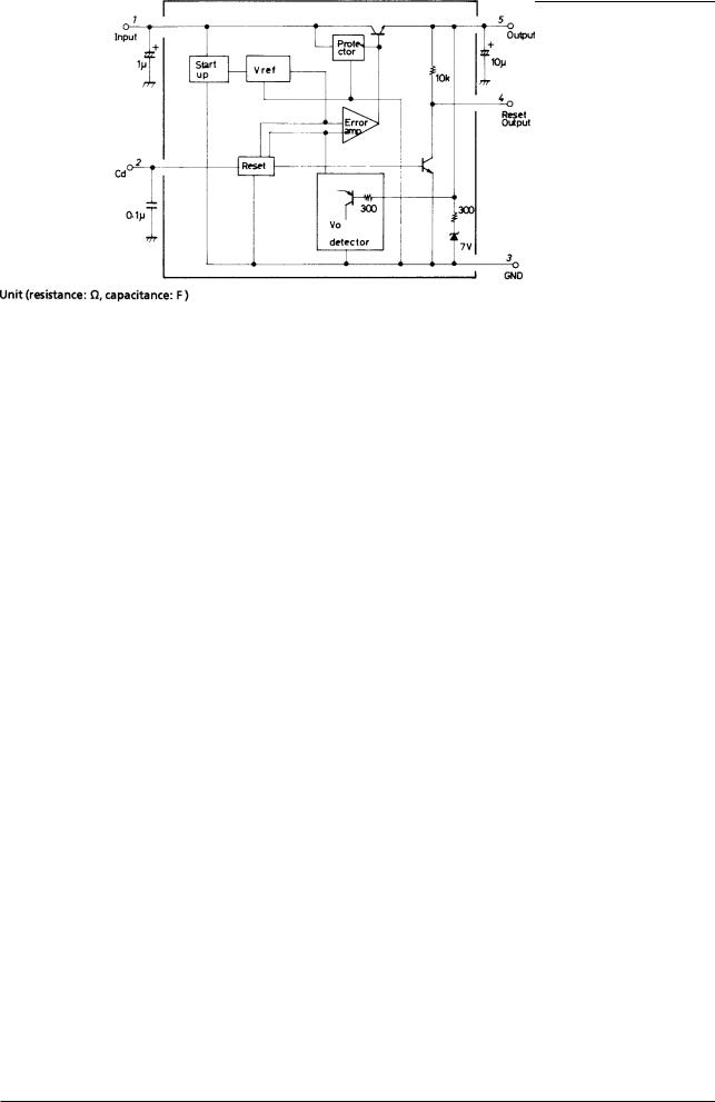
Equivalent Circuit Block Diagram
No.2622–2/6
 Loading...