


Richtek RT8251GQW, RT8251GSP Schematic [ru]

®
5A, 24V, 570kHz Step-Down Converter
RT8251
General Description
The RT8251 is a monolithic step-down switch mode
converter with a built-in internal power MOSFET . It a chieves
5A continuous output current over a wide input supply
range with excellent load a nd line regulation. Current mode
operation provides fast tra nsient response a nd ea ses loop
stabilization.
The RT8251 provides protection functions such as
cycle-by-cycle current limiting and thermal shutdown. In
shutdown mode, the regulator draws 25μA of supply
current. Programmable soft-start minimizes the inrush
supply current and the output overshoot at initial startup.
The RT8251 requires a minimum number of external
components. The RT8251 is available in WQ F N-16L 3x3
and SOP-8 (Exposed Pad) pa ckages.
Pin Configurations
(TOP VIEW)
Features
zz
Wide Operating Input Voltage Range : 4.75V to 24V
z
zz
zz
z Adjustable Output Voltage Range : 0.8V to 15V
zz
zz
z Output Current up to 5A
zz
μμ
zz
z 25
μA Low Shutdown Current
zz
μμ
zz
z Internal Power MOSFET : 70m
zz
zz
z High Efficiency up to 95%
zz
zz
z 570kHz Fixed Switching Frequency
zz
zz
z Stable with Low ESR Output Ceramic Capacitors
zz
zz
z Thermal Shutdown Protection
zz
zz
z Cycle-By-Cycle Over Current Protection
zz
zz
z RoHS Compliant and Halogen Free
zz
ΩΩ
Ω
ΩΩ
Applications
z Distributed Power Systems
z Battery Charger
z DSL Modems
z Pre-regulator for Linear Regulators
VIN
VINSWSW
VIN
1
2
VIN
VIN
GND
GND
3
4
FB
COMP
WQFN-16L 3x3
BOOT
VIN
SW
GND
2
GND
3
4
SOP-8 (Exposed Pad)
17
EN
13141516
SW
12
11
SW
10
SW
BOOT
9
8765
SS
Ordering Information
RT8251
Package Type
QW : WQFN-16L 3x3 (W-Type)
SP : SOP-8 (Exposed Pad-Option 1)
Lead Plating System
G : Green (Halogen Free and Pb Free)
Note :
Richtek products are :
` RoHS compliant and compatible with the current require-
8
SS
7
EN
6
9
COMP
5
FB
ments of IPC/JEDEC J-STD-020.
` Suitable for use in SnPb or Pb-free soldering processes.
Copyright 2013 Richtek Technology Corporation. All rights reserved. is a registered trademark of Richtek Technology Corporation.
©
DS8251-04 February 2013 www.richtek.com
1

RT8251
Marking Information
RT8251GQW
GE= : Product Code
GE=YM
DNN
Typical Application Circuit
YMDNN : Date Code
RT8251GSP
RT8251
GSPYMDNN
RT8251GSP : Product Number
YMDNN : Date Code
4.75V to 24V
V
Chip Enable
4.75V to 24V
Chip Enable
IN
C
10µF x 2
C
SS
10nF
Exposed Pad (17)
V
IN
C
SS
10nF
Exposed Pad(9)
1, 2, 3,
15, 16
IN
VIN
RT8251
7
EN
8
SS
4,
GND
BOOT
SW
FB
COMP
9
10 to 14
5
2.2nF
6
C
C
(Open)
C
C
100nF
D
B540C
R
22k
P
BOOT
C
L
4.7µH
Figure 1. T ypical Application Circuit for WQFN-16L 3x3
C
IN
10µF x 2
2
VIN
RT8251
7
EN
8
SS
4,
GND
BOOT
SW
FB
COMP
1
C
BOOT
100nF
3
D
B540C
5
C
C
2.2nF
6
4.7µH
R
C
22k
L
R1
30.9k
R2
10k
R1
30.9k
R2
10k
C
OUT
22µF x 2
V
3.3V/5A
C
OUT
22µF x 2
V
OUT
3.3V/5A
OUT
C
P
NC
Figure 2. T ypical Application Circuit for SOP-8 (Exposed Pa d)
Table 1. Recommended Component Selection
V
(V) R1 (kΩ) R2 (kΩ) RC (kΩ) CC (nF) L1 (μH) C
OUT
OUT
(μF)
15 182 10 51 1 22 44
10 115 10 43 1.2 10 44
8 91 10 39 1.5 10 44
5 52.3 10 30 1.5 6.8 44
3.3 30.9 10 22 2.2 4.7 44
2.5 21.5 10 16 2.2 4.7 44
1.8 12.4 10 13 2.2 2.2 44
1.2 4.99 10 13 2.2 2.2 44
Copyright 2013 Richtek Technology Corporation. All rights reserved. is a registered trademark of Richtek Technology Corporation.
2
©
DS8251-04 February 2013www.richtek.com

Functional Pin Description
Pin No.
WQFN-16L 3x3
1, 2, 3, 15, 16 2 VIN
4,
17 (Exposed Pad )
5 5 FB
6 6 COMP
7 7 EN
8 8 SS
9 1 BOOT
10, 11, 12, 13,
14
SOP-8
(Exposed Pad)
4,
9 (Exposed Pad)
3 SW
Pin Name Pin Function
GND
RT8251
Power Input. VIN supplies the power to the IC, as well as the
step-down converter switches. Connect VIN with a 4.75V to 24V
power source. Connect VIN to GND with a capacitor that the
capacitance is large enough to eliminate noise on the input to the
IC.
Ground. This pin is the voltage reference for the regulated output
voltage. For this reason, care must be taken in its layout. This
node should be placed outside of the D1 to C
prevent switching current spikes from inducing voltage noise into
the part. The exposed pad must be soldered to a large PCB and
connected to GND for maximum power dissipation.
Feedback Input. An external resistor divider from the output to
GND, tapped to the FB pin, sets the output voltage.
Compensation Node. This node is the output of the
transconductance error amplifier and the input to the current
comparator. Frequency compensation is done at this node by
connecting a series R-C to ground.
Enable Input. EN is a digital input that turns the regulator on or
off. Drive EN higher than 1.4V to turn on the regulator, lower
than 0.4V to turn it off. For automatic startup, leave EN
unconnected.
Soft-Start Control Input. SS controls the soft start period.
Connect a capacitor (≧ 10nF) from SS to GND to set the
soft-start period. A 10nF capacitor sets the Soft-Start period to
1ms.
Bootstrap. This capacitor C
switch’s gate above the supply voltage. It is connected between
the SW and BS pins to form a floating supply across the power
switch driver. The voltage across C
supplied by the internal +5V supply when the SW pin voltage is
low.
Power Switching Output. SW is the switching node that supplies
power to the output. Connect the output LC filter from SW to the
output load. Note that a capacitor is required from SW to BOOT
to power the high-side switch.
is needed to drive the power
BOOT
BOOT
ground path to
IN
is about 5V and is
Copyright 2013 Richtek Technology Corporation. All rights reserved. is a registered trademark of Richtek Technology Corporation.
DS8251-04 February 2013 www.richtek.com
©
3
RT8251
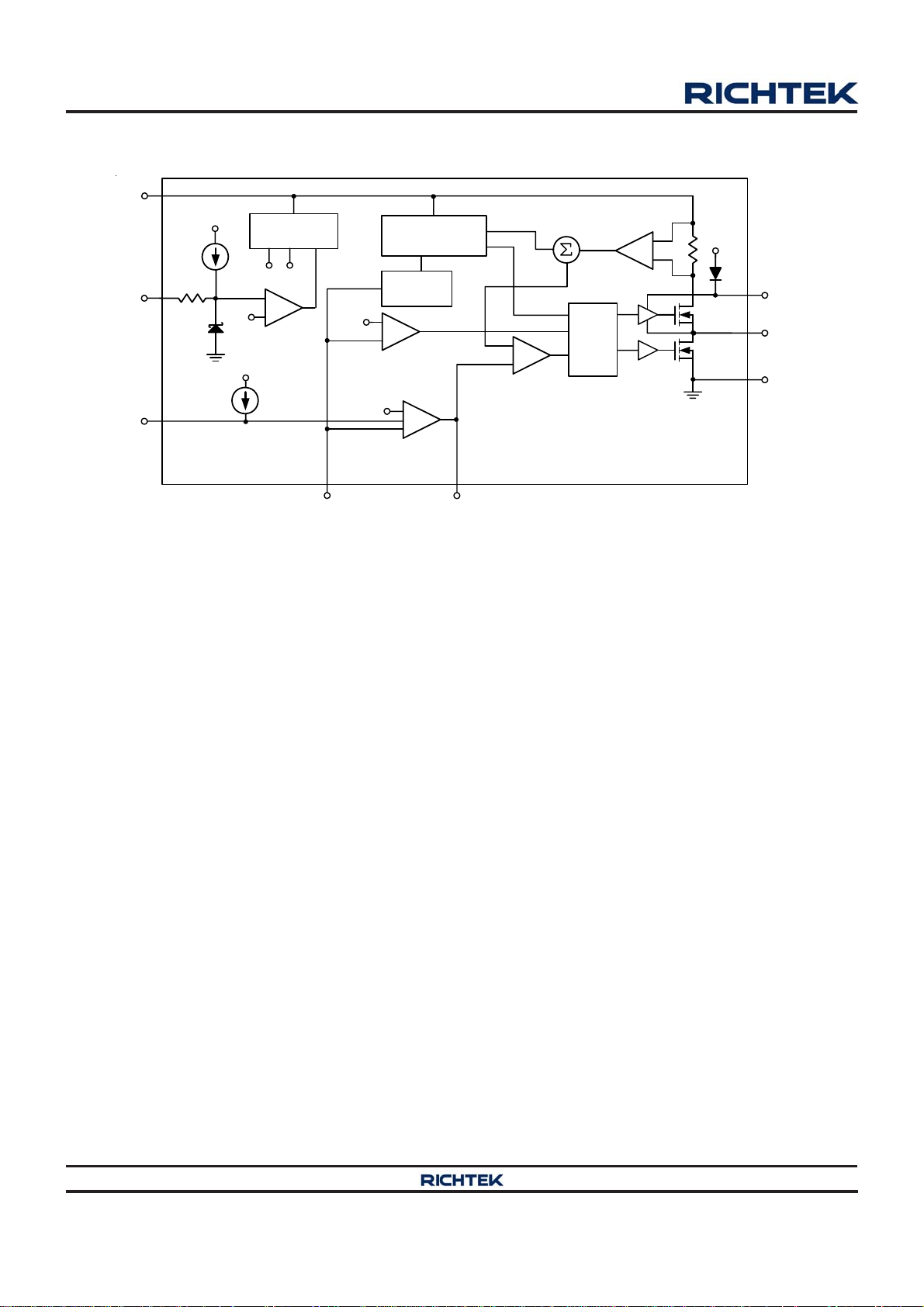
Function Block Diagram
VIN
EN
SS
1µA
10k
3V
V
CC
1.1V
Regulator
VA
-
+
Shutdown
Comparator
V
CC
10µA
Internal
V
CC
0.4V
Comparator
0.8V
Gm = 820µA/V
FB
Oscillator
570kHz
Foldback
Control
+
-
UV
+
EA
+
-
COMP
Slope Comp
+
Current
Comparator
Current Sense
Amplifier
Logic
+
-
VA
Absolute Maximum Ratings (Note 1)
z Supply Voltage, V
z Switching Voltage, V
z BOOT V oltage, V
z All Other Pins -------------------------------------------------------------------------------------------------−0.3V to 6V
z Power Dissipation, P
WQFN-16L 3x3 -----------------------------------------------------------------------------------------------1.471W
SOP-8 (Exposed Pad) --------------------------------------------------------------------------------------1.333W
z Package Thermal Re sistance (Note 2)
WQF N-16L 3x3, θJA------------------------------------------------------------------------------------------68°C/W
WQFN-16L 3x3, θJC-----------------------------------------------------------------------------------------7.5°C/W
SOP-8 (Exposed pad), θJA---------------------------------------------------------------------------------75°C/W
SOP-8 (Exposed Pad), θJC--------------------------------------------------------------------------------15°C/W
z Junction T emperature----------------------------------------------------------------------------------------150°C
z Lead T e mperature (Soldering, 10 sec.)------------------------------------------------------------------260 °C
z Storage T emperature Range -------------------------------------------------------------------------------−65°C to 150°C
z ESD Susceptibility (Note 3)
HBM (Human Body Model)---------------------------------------------------------------------------------2kV
------------------------------------------------------------------------------------------−0.3V to 26V
IN
-------------------------------------------------------------------------------------−0.3V to (VIN + 0.3V)
SW
---------------------------------------------------------------------------------------(V
BOOT
@ TA = 25°C
D
− 0.3V) to (V
SW
BOOT
SW
GND
SW
+ 6V)
Recommended Operating Conditions (Note 4)
z Supply Voltage, V
z Enable Voltage, V
z Junction T emperature Range-------------------------------------------------------------------------------−40°C to 125°C
z Ambient T emperature Range-------------------------------------------------------------------------------−40°C to 85°C
Copyright 2013 Richtek Technology Corporation. All rights reserved. is a registered trademark of Richtek Technology Corporation.
©
4
------------------------------------------------------------------------------------------4.75V to 24V
IN
-----------------------------------------------------------------------------------------0V to 5.5V
EN
DS8251-04 February 2013www.richtek.com

RT8251
Electrical Characteristics
(VIN = 12V, TA = 25°C unless otherwise specified)
Parameter Symbol Test Conditions Min Typ Max Unit
Feedb ack Ref eren ce V olt age VFB 4.75V ≦ VIN ≦ 24V 0.784 0.8 0.816 V
High-Side Switch-On Resistance R
Low -Side Swi tch -On Res is tanc e R
DS(ON)1
DS(ON)2
High-Side Switch Leakage V
Current Limit I
LIM
Current Sense Transconductance GCS Output Current to V
Erro r Amplifi er T ansc onduct ance gm ΔIC = ±10μA -- 920 -- μA/V
Oscillator Frequency fSW 420 570 720 kHz
Short Circuit Oscillation Frequency V
Maximum Duty Cycle D
MAX
Mini mum On- Ti me tON -- 100 -- ns
UVLO Threshold Rising -- 4.1 -- V
UVL O Thresh old Hyst eresis -- 200 -- mV
Logic Low VIL -- -- 0.4
EN Input Voltage
Logic High V
IH
Enable Pu l l Up Cu r r en t V
Shutdown Current I
SHDN
Quies cen t Curr ent IQ V
Soft-Start Current ISS V
Soft-Start Period C
Thermal Shutdown TSD -- 150 -- °C
Note 1. Stresses beyond those listed “Absolute Maximum Ratings” may cause permanent damage to the device. These are
stress ratings only, and functional operation of the device at these or any other conditions beyond those indicated in
the operational sections of the specifications is not implied. Exposure to absolute maximum rating conditions may
affect device reliability.
Note 2. θ
Note 3. Devices are ESD sensitive. Handling precaution is recommended.
Note 4. The device is not guaranteed to function outside its operating conditions.
is measured at T
JA
measured at the exposed pad of the package.
= 25°C on a high effective thermal conductivity four-layer test board per JEDEC 51-7. θJC is
A
-- 70 -- mΩ
-- 15 -- Ω
= 0V, V
EN
Duty = 85%; V
= 0V -- 185 -- kHz
FB
V
= 0.7V -- 85 -- %
FB
= 0V -- -- 10 μA
SW
BOOT−SW
= 4.8V -- 6.8 -- A
-- 4.6 -- A/V
COMP
1.4 -- 5.5
= 0V -- 1 -- μA
EN
VEN = 0V -- 25 -- μA
= 2V, VFB = 1V -- 0.8 1 mA
EN
= 0V -- 10 -- μA
SS
= 10nF -- 1 -- ms
SS
V
Copyright 2013 Richtek Technology Corporation. All rights reserved. is a registered trademark of Richtek Technology Corporation.
DS8251-04 February 2013 www.richtek.com
©
5
RT8251
)
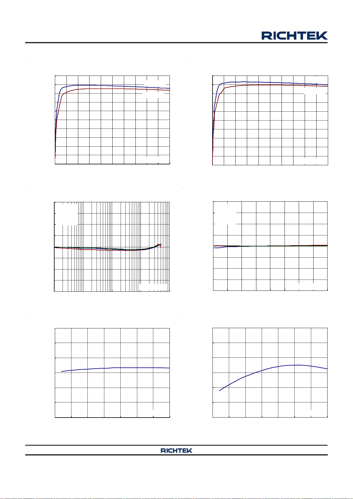
Typical Operating Characteristics
Efficiency vs. Load Current
100
90
80
70
60
50
40
Eff iciency (%)
30
20
10
0
00.511.522.533.544.55
VIN = 24V
V
Load Current (A)
Output Voltag Deviation vs. Load Current
2
VIN = 24V
1.5
0.5
1
= 12V
V
IN
VIN = 5V
VIN = 12V
= 3.3V
OUT
Efficiency vs. Load Current
100
90
80
70
60
50
40
Efficiency(%)
30
20
10
0
0 0.5 1 1.5 2 2.5 3 3.5 4 4.5 5
VIN = 24V
V
OUT
Load Current (A)
Output Voltage Deviation vs. Input Voltage
2
I
= 5A
OUT
1.5
I
= 3A
OUT
= 0A
I
OUT
1
0.5
VIN = 12V
= 5V
Reference Volt age (V)
0
-0.5
-1
-1.5
Output Voltage Deviati on (%) 1
-2
4 6.5 9 11.5 14 16.5 19 21.5 24
V
Inpu t Volt age (V)
Reference Voltage vs. Temperature
0.816
0.811
0.806
0.801
0.796
0.791
0.786
-50 -25 0 25 50 75 100 125
Temperature (°C)
= 3.3V
OUT
VIN = 12V
0
-0.5
-1
-1.5
Output V oltage Deviati on (%) 1
-2
0.001 0.01 0.1 1 10
V
Load Current (A)
Quiescent Current vs. Temperature
1.2
1
0.8
0.6
0.4
Quiescent C urrent (mA
0.2
0
-50 -25 0 25 50 75 100 125
Temperature (°C)
= 3.3V
OUT
VIN = 12V
Copyright 2013 Richtek Technology Corporation. All rights reserved. is a registered trademark of Richtek Technology Corporation.
©
DS8251-04 February 2013www.richtek.com
6
 Loading...