


Richtek RT8206LGQW, RT8206LZQW, RT8206MGQW, RT8206MZQW Schematic [ru]

®
High Efficiency, Main Power Supply Controller
for Notebook Computers
RT8206L/M
General Description
The RT8206L/M dual step-down, Switch-Mode Power-
Supply (SMPS) controller generates logic-supply voltages
in battery-powered systems. The RT8206L/M includes two
Pulse-Width Modulation (PWM) controllers fixed at 5V/
3.3V or adjustable from 2V to 5.5V. An optional external
charge pump can be monitored through SECFB (RT8206L).
This device also features a linear regulator providing a
fixed 5V output. The linear regulator provides up to 70mA
output current with automatic linear regulator bootstrapping
to the BYP input. The RT8206L/M includes on-board
power-up sequencing, the power good outputs, internal
soft-start, and internal soft-discharge output that prevents
negative voltages on shutdown.
A constant on-time PWM control scheme operates without
sense resistors and provides 100ns response to load
transients while maintaining a relatively constant switching
frequency. The unique ultrasonic mode maintains the
switching frequency above 25kHz, which eliminates noise
in audio applications. Other features include Diode-
Emulation Mode (DEM), which maximizes efficiency in
light-load applications, and fixed frequency PWM mode,
which reduces RF interference in sensitive application.
The RT8206L/M is available in a WQFN-32L 5x5 package.
Ordering Information
RT8206
Features
zz
z Wide Input Voltage Range 6V to 25V
zz
zz
z Dual Fixed 5V/3.3V Outputs or Adjustable from 2V
zz
to 5.5V, 1.5% Accuracy
zz
z Secondary Feedback Input Maintains Charge Pump
zz
V oltage (RT8206L)
zz
z Independent Enable and Power Good
zz
zz
z 5V Fixed LDO Output : 70mA
zz
zz
z 2V Reference Voltage
zz
zz
z Constant ON-Time Control with 100ns Load Step
zz
±±
±1% : 50
±±
μμ
μA
μμ
Response
zz
z Frequency Selectable via TON Setting
zz
zz
z R
zz
Current Sensing and Progra mmable Current
DS(ON)
Limit
zz
z 4700ppm/
zz
zz
z Selectable PWM, DEM or Ultrasonic Mode
zz
zz
z Internal Soft-Start with Current Limiting and Soft-
zz
°°
°C R
°°
Current Sensing
DS(ON)
Discharge
zz
z High Efficiency Up to 97%
zz
zz
z 5mW Quiescent Power Dissipation
zz
zz
z Thermal Shutdown
zz
zz
z RoHS Compliant and Halogen Free
zz
Applications
z Notebook and Sub-Notebook Computers
z 3-Cell and 4-Cell Li+ Battery-Powered Devices
Package Type
QW : WQFN-32L 5x5 (W-Type)
Lead Plating System
G : Green (Halogen Free and Pb Free)
Z : ECO (Ecological Element with
Halogen Free and Pb free)
L : With SECFB
M : Without SECFB
Note :
Richtek products are :
` RoHS compliant and compatible with the current require-
ments of IPC/JEDEC J-STD-020.
` Suitable for use in SnPb or Pb-free soldering processes.
Copyright 2012 Richtek Technology Corporation. All rights reserved. is a registered trademark of Richtek Technology Corporation.
DS8206L/M-07 June 2012 www.richtek.com
©
1

RT8206L/M
Marking Information
RT8206LGQW
RT8206LGQW : Product Number
RT8206L
YMDNN : Date Code
GQW
YMDNN
RT8206LZQW RT8206MZQW
RT8206LZQW : Product Number
RT8206L
YMDNN : Date Code
ZQW
YMDNN
Pin Configurations
(TOP VIEW)
RT8206MGQW
RT8206M
GQW
YMDNN
RT8206M
ZQW
YMDNN
RT8206MGQW : Product Number
YMDNN : Date Code
RT8206MZQW : Product Number
YMDNN : Date Code
VOUT2
FB2
ILIM2
32 31 30 29
1
REF BOOT2
2
TON
3
VCC
NC
VIN
LDO
NC
4
5
6
7
8
9101112 1413
BYP
VOUT1
ENLDO
FB1
SKIP
GND
ILIM1
PGOOD2
28 27 26 25
PGOOD1
EN2
33
EN1
PHASE2
UGATE2
24
23
22
21
20
19
18
17
1615
PHASE1
UGATE1
WQFN-32L 5x5
RT8206L
LGATE2
PGND
GND
SECFB
PVCC
LGATE1
BOOT1
VOUT2
FB2
ILIM2
32 31 30 29
1
REF BOOT2
2
TON
3
VCC
NC
VIN
LDO
NC
4
5
6
7
8
9101112 1413
BYP
VOUT1
ENLDO
FB1
SKIP
GND
ILIM1
PGOOD2
28 27 26 25
PGOOD1
EN2
33
EN1
PHASE2
UGATE2
24
23
22
21
20
19
18
17
1615
PHASE1
UGATE1
WQFN-32L 5x5
RT8206M
LGATE2
PGND
GND
NC
PVCC
LGATE1
BOOT1
Copyright 2012 Richtek Technology Corporation. All rights reserved. is a registered trademark of Richtek Technology Corporation.
©
DS8206L/M-07 June 2012www.richtek.com
2

Typical Application Circuit
C
1
1
µ
F
0
Q1
L
1
µ
H
.
8
V
1
T
U
O
V
5
3
C
2
µ
F
0
2
6
5
R
4
C
6
C
0
.
8
C
0
.
2
D
1
µ
F
D
4
1
µ
F
CP
Q3
C
1
D
D
V
P
0
3
0
1
R
1
2
0
0
k
9
C
1
C
C
R
R
C
2
F
µ
1
.
0
5
.
1
µ
F
7
C
.
1
µ
F
2
1
R
3
9
k
R
7
RT8206L/M
V
N
I
o
t
6
V
2
5
4
1
R
.
9
3
8
1
C
F
µ
.
1
0
4
0
15
0
3
17
16
18
10
9
C
1
µ
F
20
11
32
19
6
1
C
0
1
C
6
VIN
UGATE1
BOOT1
PHASE1
LGATE1
9
BYP
VOUT1
3
VCC
SECFB/NC
FB1
FB2
PVCC
7
LDO
RT8206L/M
PGOOD1
PGOOD2
UGATE2
BOOT2
PHASE2
LGATE2
PGND
VOUT2
REF
EN1
EN2
ENLDO
ILIM1
ILIM2
TON
SKIP
GND
26
24
25
23
22
30
1
13
28
14
27
4
12
31
2
29
21, 33 (Exposed Pad)
9
R
0
8
0
R
Q2
C
1
1
0
1
.
µ
F
Q4
1
C
5
2
.
0
µ
F
2
5
E
V
n
a
b
e
l
3
3
.
n
E
a
V
b
l
e
L
D
O
C
o
o
r
t
n
e
F
r
q
W
P
M
R
6
1
0
0
k
1
R
3
1
0
0
k
l
R
1
1
8
0
k
R
2
1
8
0
k
u
e
n
c
C
o
y
n
o
r
t
E
D
/
l
t
U
M
/
s
a
r
1
3
C
1
R
C
C
1
0
µ
L
4
7
.
1
0
1
4
V
P
P
V
2
F
1
0
µ
F
2
µ
H
C
1
7
2
2
0
C
C
C
C
ON
OFF
V
N
I
l
o
n
c
i
V
V
O
U
T
2
V
3
.
3
µ
F
Figure 1. Fixed Voltage Regulator
Copyright 2012 Richtek Technology Corporation. All rights reserved. is a registered trademark of Richtek Technology Corporation.
DS8206L/M-07 June 2012 www.richtek.com
©
3

RT8206L/M
1
C
µ
F
0
1
L
8
.
V
1
T
U
O
V
5
C
3
µ
F
0
2
2
3
2
C
0
2
C
F
µ
.
1
0
6
C
6
1
0
F
µ
.
C
8
0
1
F
µ
.
CP
5
1
R
1
5
k
6
1
R
1
0
k
V
N
I
o
6
t
V
5
2
4
1
R
.
3
9
8
1
C
F
.
µ
0
1
R
0
Q1
4
R
C
1
µ
H
Q3
R
5
4
C
2
F
.
µ
0
1
15
0
3
17
16
18
10
C
5
1
D
1
0
F
µ
.
D
2
C
7
C
3
D
1
0
F
µ
.
4
D
1
1
R
2
0
0
k
9
1
C
9
1
F
µ
20
2
1
R
3
9
k
11
V
P
C
C
R
7
19
6
C
1
0
C
1
6
VIN
UGATE1
BOOT1
PHASE1
LGATE1
9
BYP
VOUT1
3
VCC
SECFB/NC
FB1
PVCC
7
LDO
RT8206L/M
UGATE2
BOOT2
PHASE2
LGATE2
PGND
VOUT2
FB2
REF
PGOOD1
PGOOD2
EN1
EN2
ENLDO
ILIM1
ILIM2
TON
SKIP
GND
R
9
26
24
25
0
R
0
8
C
1
1
1
0
µ
.
23
22
30
32
1
C
1
5
0
2
2
.
µ
F
13
28
5
E
V
n
a
e
l
14
27
4
12
31
2
29
b
3
3
.
E
V
n
a
b
e
l
L
D
o
C
O
o
r
n
l
t
1
1
e
F
r
q
u
e
n
P
W
D
/
M
21, 33 (Exposed Pad)
Q2
F
Q4
6
R
1
0
0
k
R
1
3
1
0
0
k
R
1
8
0
k
R
2
8
0
k
c
y
o
C
n
o
r
t
E
t
U
l
/
M
a
r
s
1
C
3
C
1
1
0
µ
L
2
4
7
H
µ
.
1
R
0
C
1
4
P
V
C
C
P
V
C
C
2
F
1
0
µ
F
1
C
7
2
2
0
R
1
7
.
k
6
5
R
1
8
k
0
1
ON
OFF
V
I
N
l
o
n
c
i
V
V
O
U
T
2
3
3
V
.
F
µ
2
C
2
C
2
1
0
1
F
µ
.
Figure 2. Adjustable Voltage Regulator
Copyright 2012 Richtek Technology Corporation. All rights reserved. is a registered trademark of Richtek Technology Corporation.
4
©
DS8206L/M-07 June 2012www.richtek.com
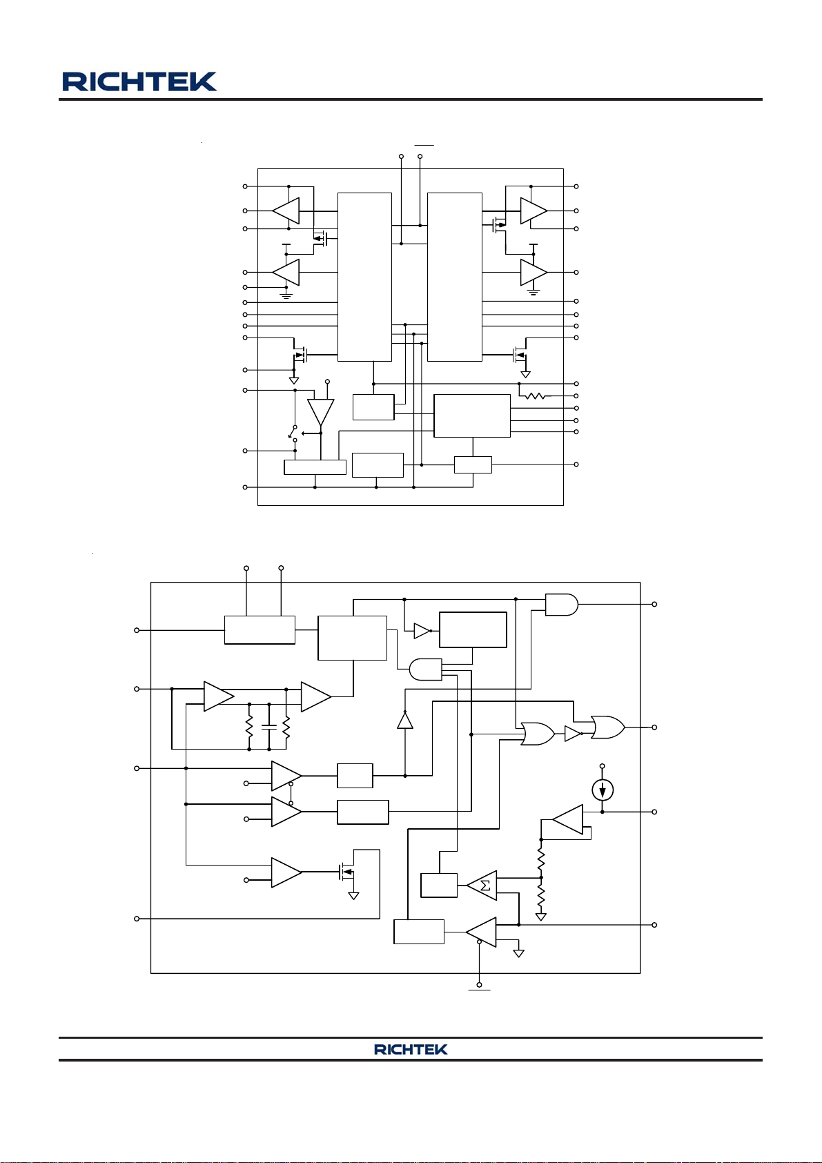
Function Block Diagram
RT8206L/M
TON SKIP
BOOT1
UGATE1
PHASE1
LGATE1
PGND
VOUT1
FB1
ILIM1
PGOOD1
GND
BYP
LDO
VIN
PV
VINTON
CC
LDO
SMPS1
PWM Buck
Controller
SW Threshold
Internal
Logic
Thermal
Shutdown
Function Block Diagram
SMPS2
PWM Buck
Controller
Power-On
Sequence
Clear Fault Latch
REF
PV
BOOT2
UGATE2
PHASE2
CC
LGATE2
VOUT2
FB2
ILIM2
PGOOD2
VCC
PVCC
ENLDO
EN1
EN2
REF
VOUT
REF
FB
PGOOD
+
1.1 x V
0.55 x V
0.9 x V
+
-
REF
REF
REF
On-Time
Compute
T
Comp
+
Over-Voltage
+
-
+
Under-Voltage
+
Q
1-Shot
R
TRIG
Q
ON
TRIG
Fault
Latch
Blanking
Time
SS
Time
25kHz
Detector
Zero
Detector
SKIP
PWM Controller (One Side)
T
OFF
1-Shot
+
-
+
-
Current
Limit
UGATE
LGATE
V
CC
+
ILIM
-
PHASE
Copyright 2012 Richtek Technology Corporation. All rights reserved. is a registered trademark of Richtek Technology Corporation.
©
DS8206L/M-07 June 2012 www.richtek.com
5

RT8206L/M
Functional Pin Description
REF (Pin 1)
2V Reference Output. Bypass to GND with a 0.22μF
capacitor. REF can source up to 50μA for external loads.
Loading REF degrades FBx and output accuracy according
to the REF load-regulation error.
TON (Pin 2)
Frequency Select Input. (VOUT1/VOUT2 switching
frequency, respectively) :
TON = VCC, (200kHz / 300kHz)
TON = REF, (300kHz / 400kHz)
TON = GND, (400kHz / 500kHz)
VCC (Pin 3)
Analog Supply Voltage Input for the PWM Core. Bypass
to GND with a 1μF ceramic capacitor
ENLDO (Pin 4)
LDO Enable Input. REF and LDO are enabled if ENLDO
is within logic high level and disabled if ENLDO is less
than the logic low level.
NC (Pin 5, 8)
No Internal Connection.
VIN (Pin 6)
Power Supply Input. VIN is used for the constant on-time
PWM one shot circuits. VIN is also used to power the
linear regulators. The linear regulators are powered by
SMPS1 if VOUT1 is set greater than 4.66V and BYP is
tied to VOUT1. Connect VIN to the battery input and
bypass with a 1μF capacitor.
LDO (Pin 7)
Linear-Regulator Output. LDO can provide a total of 70mA
external loads. The LDO regulates a fixed 5V output. When
the BYP is within 5V switchover threshold, the internal
regulator shuts down and the LDO output pin connects to
BYP through a 1.5Ω switch. Bypass LDO output with a
minimum of 4.7μF ceramic.
BYP (Pin 9)
Switchover Source Voltage Input for LDO.
VOUT1 (Pin 10)
SMPS1 Output Voltage Sense Input. Connect this pin to
the SMPS1 output. VOUT1 is an input to the constant
on-time-PWM one-shot circuit. It also serves as the
SMPS1 feedback input in fixed-voltage mode.
FB1 (Pin 1 1)
SMPS1 Feedback Input. Connect FB1 to VCC or GND for
fixed 5V operation. Connect FB1 to a resistive voltage-
divider from VOUT1 to GND to adjust output from 2V to
5.5V.
ILIM1 (Pin 12)
SMPS1 Current Limit Adjustment. The GND − PHASE1
current-limit threshold is 1/10th the voltage seen at ILIM1
over a 0.5V to 2.5V range. There is an internal 5μA current
source from VCC to ILIM1. The logic current limit threshold
defaults to 100mV if ILIM1 is higher than (VCC − 1V).
PGOOD1 (Pin 13)
SMPS1 Power Good Open-Drain Output. PGOOD1 is low
when the SMPS1 output voltage is more than 10% below
the normal regulation point or during soft-start. PGOOD1
is in high impedance when the output is in regulation and
the soft-start circuit has terminated. PGOOD1 is low in
shutdown.
EN1 (Pin 14)
SMPS1 Enable Input. The SMPS1 will be enabled if EN1
is greater than the logic high level and disabled if EN1 is
less than the logic low level. If EN1 is connected to REF,
SMPS1 starts after SMPS2 reaches regulation (delay
start). Drive EN1 below 0.8V to clear fault level and reset
the fault latches.
UGA TE1 (Pin 15)
High Side MOSFET Floating Gate-Driver Output for
SMPS1. UGATE1 swings between PHASE1 and BOOT1.
Copyright 2012 Richtek Technology Corporation. All rights reserved. is a registered trademark of Richtek Technology Corporation.
6
©
DS8206L/M-07 June 2012www.richtek.com

RT8206L/M
PHASE1 (Pin 16)
Inductor Connection for SMPS1. PHASE1 is the internal
lower supply rail for the UGATE1 high side gate driver.
PHASE1 is the current-sense input for the SMPS1.
BOOT1 (Pin 17)
Boost Flying Capacitor Connection for SMPS1. Connect
to an external capacitor according to the typical application
circuits.
LGA TE1 (Pin 18)
SMPS1 Synchronous-Rectifier Gate-drive Output. LGATE1
swings between PGND and PVCC.
PVCC (Pin 19)
Supply Voltage for Low Side MOSFET driver LGATEx.
Connect a 5V power source to the PVCC pin (bypass
with 1μF MLCC capacitor to PGND if necessary). There is
an internal 10Ω connecting from PVCC to VCC. Make
sure that both VCC and PVCC are bypassed with 1μF
MLCC capacitors.
SECFB (Pin 20) (RT8206L)
Charge Pump Feedback Input. The SECFB is used to
monitor the optional external charge pump. Connect a
resistive voltage-divider from the charge pump output to
GND to detect the output. If SECFB drops below the
threshold voltage, an ultrasonic pulse occurs to refresh
the external charge pump driven by LGATE1 or LGATE2
NC (Pin 20) (RT8206M)
No Internal Connection.
LGA TE2 (Pin 23)
SMPS2 Synchronous-Rectifier Gate-drive Output. LGATE2
swings between PGND and PVCC.
BOOT2 (Pin 24)
Boost Flying Capacitor Connection for SMPS2. Connect
this pin to an external capacitor according to the typical
application circuits.
PHASE2 (Pin 25)
Inductor Connection for SMPS2. PHASE2 is the internal
lower supply rail for the UGATE2 high side gate driver.
PHASE2 is the current sense input for the SMPS2.
UGA TE2 (Pin 26)
High Side MOSFET Floating Gate-Driver Output for
SMPS2. UGATE2 swings between PHASE2 and BOOT2.
EN2 (Pin 27)
SMPS2 Enable Input. The SMPS2 will be enabled if EN2
is greater than the logic high level and be disabled if EN2
is less than the logic low level. If EN2 is connected to
REF, the SMPS2 starts after the SMPS1 reaches
regulation (delay start). Drive EN2 below 0.8V to clear
fault level and reset the fault latches.
PGOOD2 (Pin 28)
SMPS2 Power Good Open-Drain Output. PGOOD2 is low
when the SMPS2 output voltage is more than 10% below
the normal regulation point or during soft-start. PGOOD2
is high impedance when the output is in regulation and
the soft-start circuit has terminated. PGOOD2 is low in
shutdown.
GND [Pin 21, 33 (Exposed Pad)]
Analog Ground for both SMPS and LDO. The exposed
pad must be soldered to a large PCB and connected to
GND for maximum power dissipation.
PGND (Pin 22)
Power Ground for SMPS Controller. Connect PGND
externally to the underside of the exposed pad.
Copyright 2012 Richtek Technology Corporation. All rights reserved. is a registered trademark of Richtek Technology Corporation.
DS8206L/M-07 June 2012 www.richtek.com
©
SKIP (Pin 29)
SMPS Operation Mode Control.
SKIP = GND : DEM Mode operation
SKIP = REF : Ultrasonic Mode operation
SKIP = VCC : PWM Mode operation.
7

RT8206L/M
VOUT2 (Pin 30)
SMPS2 Output Voltage Sense Input. Connect this pin to
the SMPS2 output. VOUT2 is an input to the constant
on-time-PWM one-shot circuit. It also serves as the
SMPS2 feedback input in fixed-voltage mode.
ILIM2 (Pin 31)
SMPS2 Current-Limit Adjustment. The GND − PHASE2
current limit threshold is 1/10th the voltage seen at ILIM2
over a 0.5V to 2.5V range. There is an internal 5μA current
source from VCC to ILIM2. The logic current limit threshold
is default to 100mV value if ILIM2 is higher than (VCC −
1V).
FB2 (Pin 32)
SMPS2 Feedback Input. Connect FB2 to VCC or GND for
fixed 3.3V operation. Connect FB2 to a resistive voltage-
divider from VOUT2 to GND to adjust output from 2V to
5.5V.
Copyright 2012 Richtek Technology Corporation. All rights reserved. is a registered trademark of Richtek Technology Corporation.
8
©
DS8206L/M-07 June 2012www.richtek.com

RT8206L/M
Absolute Maximum Ratings (Note 1)
z VIN, ENLDO to GND -------------------------------------------------------------------------------------------- –0.3V to 30V
z PHASEx to GND
DC ------------------------------------------------------------------------------------------------------------------- −0.3V to 30V
<20ns -------------------------------------------------------------------------------------------------------------- −8V to 38V
z BOOTx to PHASEx --------------------------------------------------------------------------------------------- −0.3V to 6V
z VCC, ENx, SKIP, TON, PVCC, PGOODx, to GND ----------------------------------------------------- −0.3V to 6V
z LDO, FBx, VOUTx, SECFB, REF, ILIMx to GND -------------------------------------------------------- −0.3V to (V
z UGATEx to PHASEx
DC ------------------------------------------------------------------------------------------------------------------- −0.3V to (PVCC + 0.3V)
<20ns -------------------------------------------------------------------------------------------------------------- −5V to 7.5V
z LGATEx, BYP to GND
DC ------------------------------------------------------------------------------------------------------------------- −0.3V to (PVCC + 0.3V)
<20ns -------------------------------------------------------------------------------------------------------------- −2.5V to 7.5V
z PGND to GND ---------------------------------------------------------------------------------------------------- −0.3V to 0.3V
z Power Dissipation, P
@ TA = 25°C
D
WQFN-32L 5x5 -------------------------------------------------------------------------------------------------- 2.778W
z Package Thermal Resistance (Note 2)
WQFN-32L 5x5, θJA--------------------------------------------------------------------------------------------- 36°C/W
WQFN-32L 5x5, θJC-------------------------------------------------------------------------------------------- 6°C/W
z Junction Temperature ------------------------------------------------------------------------------------------- 150°C
z Lead Temperature (Soldering, 10 sec.)--------------------------------------------------------------------- 260°C
z Storage Temperature Range ---------------------------------------------------------------------------------- −65°C to 150°C
z ESD Susceptibility (Note 3)
HBM (Human Body Model)------------------------------------------------------------------------------------ 2kV
+ 0.3V)
CC
Recommended Operating Conditions (Note 4)
z Input Voltage, VIN ----------------------------------------------------------------------------------------------- 6V to 25V
z Junction Temperature Range ---------------------------------------------------------------------------------- −40°C to 125°C
z Ambient Temperature Range ---------------------------------------------------------------------------------- −40°C to 85°C
Copyright 2012 Richtek Technology Corporation. All rights reserved. is a registered trademark of Richtek Technology Corporation.
DS8206L/M-07 June 2012 www.richtek.com
©
9
 Loading...