

®
RT8231A/B
Complete DDR Memory Power Supply Controller
General Description
The RT8231A/B provides a complete power supply for
DDR2/DDR3/DDR3L/LPDDR3/DDR4 memory systems. It
integrates a synchronous PWM Buck controller with a
1.5A sink/source tracking linear regulator and buffered low
noise reference.
The PWM controller provides the low quiescent current,
high efficiency, excellent transient response, and high DC
output accuracy needed for stepping down high-voltage
batteries to generate low-voltage chipset RAM supplies
in notebook computers. The constant on-time PWM
control scheme handles wide input/output voltage ratios
with ease and provides 100ns “instant-on” response to
load transients while maintaining a relatively constant
switching frequency.
The RT8231A/B achieves high efficiency at a reduced cost
by eliminating the current-sense resistor found in
traditional current mode PWMs. Efficiency is further
enhanced by its ability to drive very large synchronous
rectifier MOSFETs. The Buck conversion allows this device
to directly step down high-voltage batteries for the highest
possible efficiency.
The 1.5A sink/source LDO maintains fast transient
response only requiring a 10μF ceramic output capacitor.
In addition, the LDO supply input is available externally
to significantly reduce the total power losses. The
RT8231A/B supports all of the sleep state controls placing
VTT at high-Z in S3 and discharging VDDQ, VTT and
VTTREF (soft-off) in S4/S5.
The RT8231A/B provides protections including OVP, UVP,
and thermal shutdown. The RT8231A/B is available in the
WQFN-20L 3x3 package.
Applications
DDR2/DDR3/DDR3L/LPDDR3/DDR4 Memory Power
Supplies
Notebook computers
SSTL18, SSTL15 and HSTL bus termination
Pin Configurations
(TOP VIEW)
BOOT
VLDOIN
S3
S5
PHASE
16
17181920
15
LGATE
14
PGND
13
CS
12
21
9876
TON UGATE
VDD
115
VID
10
PGOOD
VTTGND
VTTSNS
GND
VTTREF
VDDQ
VTT
1
2
3
GND
4
FB
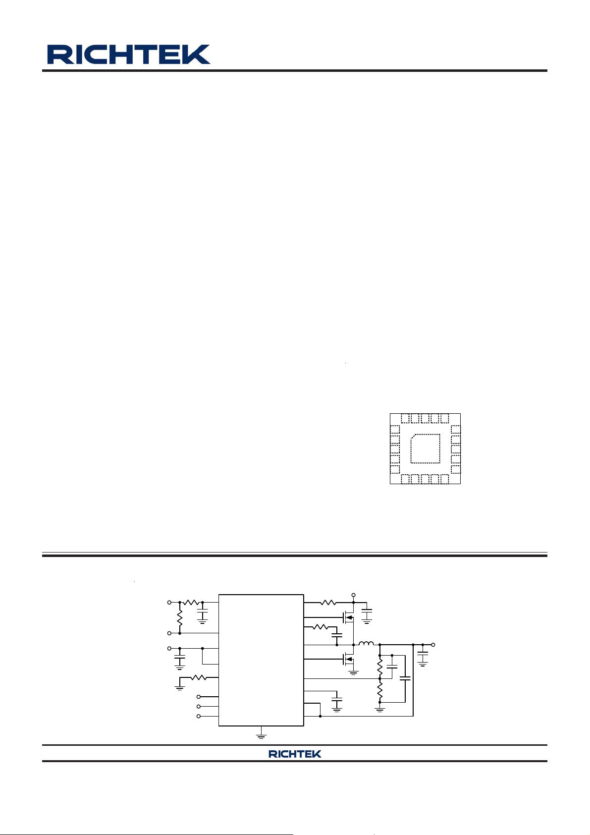
WQFN-20L 3x3
Simplified Application Circuit
V
IN
V
VDD
V
TT
Copyright 2015 Richtek Technology Corporation. All rights reserved. is a registered trademark of Richtek Technology Corporation.
©
VDD
PGOODPGOOD
VTT
VTTSNS
CS
S3
S5
VID
RT8231A/B
GND
DS8231A/B-05 March 2015 www.richtek.com
TON
UGATE
BOOT
PHASE
LGATE
FB
VTTREF
VDDQ
VLDOIN
V
D
V
D
Q
1
RT8231A/B
Features
PWM Controller
Adjustable Current Limit with Low-Side R
Sensing
Low Quiescent Supply Current
Quick Load-Step Response within 100ns
1% V
Adjustable 0.675V to 3.3V Output Range for 1.8V
(DDR2), 1.5V (DDR3), 1.35V (DDR3L), 1.2V (LPDDR3)
and 1.2V (DDR4)
4.5V to 26V Battery Input Range
Resistor Adjustable Frequency
Over-/Under-Voltage Protection
Internal Voltage Ramp Soft-Start
Drives Large Synchronous Re ctifier MOSFETs
Power Good Indicator
1.5A LDO (VTT), Buffered Reference (VTTREF)
Capable to Sink and Source Up to 1.5A
LDO Input Available to Optimize Power Losses
Requires Only 10
Integrated Divider Tracks 1/2 VDDQ for both VTT
and VTTREF
Accuracy
Supports High-Z in S3 and Soft-Off in S4/S5
RoHS Compliant and Halogen Free
Accuracy Over Line and Load
VDDQ
μμ
μF Ceramic Output Capacitor
μμ
±±
±20mV for both VTTREF and VTT
±±
DS(ON)
Ordering Information
RT8231A/B
Package Type
QW : WQFN-20L 3x3 (W-Type)
Lead Plating System
G : Green (Halogen Free and Pb Free)
VDDQ and VTT Discharge Control
A : Tracing Mode
B : Non-Tracking Mode
Note :
Richtek products are :
RoHS compliant and compatible with the current require-
ments of IPC/JEDEC J-STD-020.
Suitable for use in SnPb or Pb-free soldering processes.
Marking Information
RT8231AGQW
24= : Product Code
24=YM
DNN
RT8231BGQW
3T=YM
DNN
YMDNN : Date Code
3T= : Product Code
YMDNN : Date Code
Copyright 2015 Richtek Technology Corporation. All rights reserved. is a registered trademark of Richtek Technology Corporation.
©
DS8231A/B-05 March 2015www.richtek.com
2
Functional Pin Description
Pin No. Pin Name Pin Function
1 VTTGND Power Grou nd for the VTT LDO.
RT8231A/B
2 VTTSNS
3, 21
(Exposed Pad)
4 VTTREF VTTREF Buffered Reference Output.
5 VDDQ Reference Input for VTT and VTTREF.
6 FB
7 S3 VTT LDO Enable Control Input. Do not leave this pin floating.
8 S5 PWM Enable Co ntrol In put. Do n ot leave thi s pin floati ng.
9 TON Set the UGATE On-Time Through a Pul l-Up Resistor Connectin g to VIN.
10 PGOOD
11 VID Internal Reference Voltage Setting.
12 VDD Su pply Voltage Input for the Analog Supply and LGATE Gate Driver.
13 CS
14 PGND Power Ground for Low-Side MOSFET.
15 LGATE Low-Sid e Gate Driver Output for VDDQ.
GND
Voltage Sense Input for the VTT LDO. Connect to the terminal of the VTT_LDO
output capacitor.
The exposed pad must be soldered to a large PCB and connected to GND for
maximum power dissipation.
Feedback Voltage Inpu t. Conn ect to a resistive v oltage divi der fr om VDDQ to
GND to adjust the output voltage .
Power Good Open-Drain Output. In high state when VDDQ output voltage i s
within the target range.
Current Limit Threshold Setting Input. Conn ect to GND th rou gh the voltag e
setting resistor.
16 PHASE
17 UGAT E High-Side Gate Driver Output for VDDQ.
18 BOOT Bootstrap Sup ply for High-Sid e Gate Driver.
19 VLDOIN Power Supply for VTT LDO.
20 VTT Power Output for the VTT LDO.
Swit ch Node. External i nductor conne ction f or VDDQ an d behave as the curre nt
sen se comparat or in put for Low-Side MOSFET R
DS(ON)
sen sing.
Copyright 2015 Richtek Technology Corporation. All rights reserved. is a registered trademark of Richtek Technology Corporation.
DS8231A/B-05 March 2015 www.richtek.com
©
3
RT8231A/B
Function Block Diagram
Buck Controller
TRIG
REF
On-Time
1-SHOT
+
-
+
-
SS Timer
V
OV
UV
85% V
VDDQ
TON
115%V
FB
0.45V
SS Int
S5
REF
Comp
+
+
-
Latch
S1 Q
Latch
S1 Q
-
+
REF
Thermal
Shutdown
Reference
Voltage
Selector
BOOT
R
QS
Min. T
OFF
TRIG
DEM
+
1/10
-
V
REF
5µA
UGATE
PHASE
VDD
LGATE
PGND
CS
VTT LDO
S5
S3
GND
VTTSNS
VDD
Non-Tracking
Discharge
VID
VDDQ
Thermal
Shutdown
+
-
PGOOD
+
-
VTTREF
VLDOIN
+
-
VTT
+
-
VTTGND
Copyright 2015 Richtek Technology Corporation. All rights reserved. is a registered trademark of Richtek Technology Corporation.
©
DS8231A/B-05 March 2015www.richtek.com
4
Operation
RT8231A/B
The RT8231A/B is a constant on-time synchronous step-
down controller. In normal operation, the high-side
N-MOSFET is turned on when the output voltage is lower
than VREF, and is turned off after the internal one-shot
timer expires. While the high-side N-MOSFET is turned
off, the low-side N-MOSFET is turned on to conduct the
inductor current until next cycle begins.
Soft-Start (SS)
For internal soft-start function, an internal current source
charges an internal capacitor to build the soft-start ramp
voltage. The output voltage will track the internal ramp
voltage during soft-start interval.
PGOOD
The power good output is an open-drain architecture. When
the soft-start is finished, the PGOOD open-drain output
will be high impedance.
Current Limit
The current limit circuit employs a unique “valley” current
sensing algorithm. If the magnitude of the current sense
signal at PHASE is above the current limit threshold, the
PWM is not allowed to initiate a new cycle. The current
limit threshold can be set with an external voltage setting
resistor on the CS pin.
Over-Voltage Protection (OVP) & Under-Voltage
Protection (UVP)
The output voltage is continuously monitored for over-
voltage and under-voltage protection. When the output
voltage exceeds its set voltage threshold( 115% of V
UGATE goes low and LGATE is forced high. When the
feedback voltage is less than 0.45V, under-voltage
protection is triggered and then both UGATE and LGATE
gate drivers are forced low. The controller is latched until
VDD is re-supplied and exceeds the POR rising threshold
voltage or S5 is reset.
VTT Linear Regulator and VTTREF
This VTT linear regulator employs ultimate fast response
feedback loop so that small ceramic capacitors are enough
for keeping track of VTTREF within 40mV at all conditions,
including fast load transient. The VTTREF block consists
of on-chip 1/2 divider, LPF and buffer. This regulator also
has sink and source capability up to 10mA. Bypass
VTTREF to GND with a 33nF ceramic capacitor for stable
operation.
OUT
),
Copyright 2015 Richtek Technology Corporation. All rights reserved. is a registered trademark of Richtek Technology Corporation.
DS8231A/B-05 March 2015 www.richtek.com
©
5
RT8231A/B
Absolute Maximum Ratings (Note 1)
Supply Input Voltage, TON to GND ------------------------------------------------------------------------------------ −0.3V to 32V
BOOT to PHASE ---------------------------------------------------------------------------------------------------------- −0.3V to 6V
PHASE to GND
DC----------------------------------------------------------------------------------------------------------------------------- −0.3V to 32V
< 20ns ----------------------------------------------------------------------------------------------------------------------- −8V to 38V
LGATE to GND
DC----------------------------------------------------------------------------------------------------------------------------- −0.3V to 6V
< 20ns ----------------------------------------------------------------------------------------------------------------------- −2.5V to 7.5V
UGATE to PHASE
DC----------------------------------------------------------------------------------------------------------------------------- −0.3V to 6V
< 20ns ----------------------------------------------------------------------------------------------------------------------- −5V to 7.5V
VDD, CS, S3, S5, VTTSNS, VDDQ, VID, VTTREF, VTT, VLDOIN, FB, PGOOD to GND ---------------- −0.3V to 6V
PGND, VTTGND to GND ------------------------------------------------------------------------------------------------- −0.3V to 0.3V
Other Pins------------------------------------------------------------------------------------------------------------------- −0.3V to 6.5V
Power Dissipation, P
WQFN-20L 3x3 ------------------------------------------------------------------------------------------------------------ 3.33W
Package Thermal Resistance (Note 2)
WQFN-20L 3x3, θJA------------------------------------------------------------------------------------------------------- 30°C/W
WQFN-20L 3x3, θJC------------------------------------------------------------------------------------------------------ 7.5°C/W
Junction Temperature ----------------------------------------------------------------------------------------------------- 150°C
Lead Temperature (Soldering, 10 sec.)------------------------------------------------------------------------------- 260°C
Storage Temperature Range -------------------------------------------------------------------------------------------- −65°C to 150°C
ESD Susceptibility (Note 3)
HBM (Human Body Model)---------------------------------------------------------------------------------------------- 2kV
@ T
D
= 25°C
A
Recommended Operating Conditions (Note 4)
Input Voltage, VIN --------------------------------------------------------------------------------------------------------- 4.5V to 26V
Control Voltage, VDD ----------------------------------------------------------------------------------------------------- 4.5V to 5.5V
Junction Temperature Range -------------------------------------------------------------------------------------------- −40°C to 125°C
Ambient Temperature Range -------------------------------------------------------------------------------------------- −40°C to 85°C
Electrical Characteristics
(VDD = 5V, V
PWM Controller
Quiescent S upp ly Current
TON Operati ng Current R
I
VLDOIN
I
VLDOIN
Copyright 2015 Richtek Technology Corporation. All rights reserved. is a registered trademark of Richtek Technology Corporation.
6
= 12V, R
IN
= 620kΩ, TA = 25°C, unless otherwise specified)
TON
Parameter Symbol Test Conditions Min Typ Max Unit
FB Forced above the Regulation Point,
V
= 5V, VS3 = 0V, Not Switching
S5
= 620k, VIN = 12V -- 19 -- A
TON
-- 135 -- A
BIAS Current VS5 = VS3 = 5V, VTT = No Load -- 1 -- A
Standby Current VS5 = 5V, VS3 = 0, VTT = No Load -- 0.1 10 A
©
DS8231A/B-05 March 2015www.richtek.com
RT8231A/B
Parameter Symbol Test Conditions Min Typ Max Unit
VDD -- 0.1 10 A
TON -- 0.1 5 A
Shutdown Current
= VS3 = 0V)
(V
S5
FB Error Comparator
Threshold
VDDQ Voltage Rang e 0.675 -- 3.3 V
Switch Frequency fSW
Minimum Off-Time 250 400 550 ns
VDDQ Shutdown Discharge
Resistance
Current Sensing
CS Pin Source Current 4.5 5 5.5 A
Zero Cros sing Threshol d GND PHASE 5 -- 10 mV
I
SHDN
S5/S3 1 0.1 1 A
VLDOIN -- 0.1 1 A
VID -- 0.5 1 A
V
V
REF
V
= 0.675V/ 0.75V 1 0 1 %
REF
R
= 620k, VIN = 12V,
TON
= 1 .5V, I
V
DDQ
= 0V, VS3 = 0V -- 15 --
S5
= 20A (Note 5)
OUT
320 4 00 480 kHz
Fault Protection
Current Limit (Positive) GND PHASE, RCS = 160k 70 80 90 mV
Output UV Threshold V
UVP
FB
low.
0.4 0.45 0.5 V
V
Falling. For both VID is high or
UVP Latch Delay FB Forced below UV Threshol d -- 30 -- s
OVP Threshold V
OVP
With Respect to Error Compar ator
Threshold
110 115 120 %
OVP Latch Delay FB Forced above OV Threshold -- 5 -- s
VDD POR Threshold
Rising Edge, Hysteresis = 120mV,
PWM Disabled be low this Level
3.9 4.2 4.5 V
Voltage Ramp Soft-Start Time From S5 Going High to VFB = 0.675V -- 1 -- mS
UV Blank Time From S5 Si gnal Going Hi gh -- 5 -- mS
Thermal Shutdown TSD -- 165 -- C
Driver On-Resistance
UGATE Gate Driver Source R
UGATE Gate Driver Sink R
LGATE Gate Driver So urce R
LGATE Gate Driver Si nk R
UGATEsr
UGATEsk
LGATEsr
LGATEsk
BOOT PHASE Forced to 5V -- 2.5 5
BOOT PHASE Forced to 5V -- 1.5 3
DL, High State -- 2.5 5
DL, Low State -- 0.8 1.6
LGATE Rising (Phase = 1.5V) -- 40 --
Dead Time
ns
UGATE Rising -- 40 --
Internal Boost Charging Switch
On-Resistance
VDD to BOOT, 10mA -- -- 80
Copyright 2015 Richtek Technology Corporation. All rights reserved. is a registered trademark of Richtek Technology Corporation.
DS8231A/B-05 March 2015 www.richtek.com
©
7

RT8231A/B
Parameter Symbol Test Conditions Min Typ Max Unit
Logic I/O
S3, S5 Input
Voltage
Logic-High 2 -- --
V
Logic-Low -- -- 0.8
Logic Input Current S3, S5 = VDD / GND 1 0 1 A
VID Input
Threshold Voltage
Logic-High 750 -- --
mV
Logic-Low -- -- 300
PGOOD (Upper Side Threshold Decide by OV Threshold)
Trip Threshold (Falling)
Fault Propagation Delay
Output Low Voltage I
Leakage Current I
High State, F orced to 5V -- -- 1 A
LEA K
Measured at FB, with Respect to
Reference, No Load. Hysteresis = 2%
Falling Edge, FB Forced be low
PGOOD Trip Threshold
= 1mA -- -- 0.4 V
SINK
20 15 10 %
-- 5 -- s
VTT LDO
V
VTT Output Tol eran ce V
VTT Source Current Limit I
VTT Sink Current Limit I
VTT Leakage Current I
VTTSNS Leakage Current I
DDQ
1.8V, |I
V
DDQ
1.8V, |I
VTTTOL
VTTOCLSRC
VTTOCLSNK
VTTLK
VTTSNSLK
V
DDQ
| < 1.2A
|I
VTT
V
DDQ
|I
| < 1.5A
VTT
VTT = 0V 1.6 2.6 3.6 A
VTT = V
S5 = 5V, S3 = 0V,
I
= 1mA 1 -- 1 A
SINK
= V
VTT
= V
VTT
= V
= V
DDQ
= 1.2V/1.35V/1.5V/
LDOIN
| = 0A
= 1.2V/1.35V/1.5V/
LDOIN
| < 1A
= 1.2V/1.35V,
LDOIN
= 1.5V/1.8V,
LDOIN
20 -- 20
30 -- 30
mV
40 -- 40
40 -- 40
1.6 2.6 3.6 A
V
VTT =
VDDQ
10 -- 10 A
2
VTT Discharge Current I
VTTREF Output Voltage V
VDDQ/2, VTTREF Output
Voltage Tolerance
VTTREF Source Current Limit I
DSC HRG
VTTREF
V
VTTREFTOL
VTTREFOCL
V
DDQ
V
VTT
V
VDDQ
V
LDOIN
|I
VTTREF
V
LDOIN
|I
VTTREF
V
VTTREF
= 0V, VTT = 0.5V, S5 = S3 = 0V 10 30 -- mA
V
V =
=
VTTREF
VDDQ
,
2
-- 0.75 -- V
= 1.5V
= V
| < 10mA
= V
| < 10mA
VDDQ
VDDQ
= 1.5V,
= 1.8V,
15 -- 15
18 -- 18
= 0V 10 40 80 mA
Copyright 2015 Richtek Technology Corporation. All rights reserved. is a registered trademark of Richtek Technology Corporation.
8
©
DS8231A/B-05 March 2015www.richtek.com
mV
 Loading...