

High Efficiency, Main Power Supply Controller
for Notebook Computers
RT8223A/B
General Description
The RT8223A/B dual step-down, switch-mode powersupply controller generates logic-supply voltages in
battery-powered systems. The RT8223A/B includes two
pulse-width modulation (PWM) controllers fixed at 5V/
3.3V or adjustable from 2V to 5.5V. This device also
features 2 linear regulators providing fixed 5V and 3.3V
outputs. The linear regulator each provides up to 70mA
output current with automatic linear-regulator bootstrapping
to the PWM outputs. The RT8223A/B includes on-board
power-up sequencing, the power good output, internal softstart, and internal soft-discharge output that prevents
negative voltages on shutdown.
A consta nt on-time PWM control scheme operates without
sense resistor and provides 100ns response to load
transients while maintaining a relatively consta nt switching
frequency. The unique ultrasonic mode maintains the
switching frequency above 25kHz, which eliminates noise
in audio applications. Other features include diodeemulation mode (DEM), which maximizes efficiency in
light-load a pplications, a nd fixed-frequency PWM mode,
which reduces RF interference in sensitive a pplication
Features
zz
z Wide Input Voltage Range 6V to 25V
zz
zz
z Dual Fixed 5V/3.3V Outputs or Adjustable from 2V
zz
to 5.5V, 1.5% Accuracy
zz
z Fixed 3.3V and 5V LDO Output : 70mA
zz
zz
z 2V Reference Voltage ±1% : 50
zz
zz
z Constant ON-Time Control with 100ns Load Step
zz
μμ
μA
μμ
Response
zz
z Frequency Selectable via TONSEL Setting
zz
zz
z R
zz
Current Sensing and Progra mmable Current
DS(ON)
Limit combined with Enable Control
zz
z Selectable PWM, DEM, or Ultrasonic Mode
zz
zz
z Internal Soft-Start and Soft-Discharge
zz
zz
z High Efficiency up to 97%
zz
zz
z 5mW Quiescent Power Dissipation
zz
zz
z Thermal Shutdown
zz
zz
z RoHS Compliant and Halogen Free
zz
Applications
z Notebook and Sub-Notebook Computers
z 3-Cell and 4-Cell Li+ Battery-Powered Devices
Marking Information
Ordering Information
RT8223
Package Type
For marking information, contact our sales representative
directly or through a Richtek distributor located in your
area.
QW : WQFN-24L 4x4 (W-Type)
Lead Plating System
G : Green (Halogen Free and Pb Free)
Z : ECO (Ecological Element with
Halogen Free and Pb free)
Pin Function
A : Default
B : With ENC
Note :
Richtek products are :
` RoHS compliant and compatible with the current require-
ments of IPC/JEDEC J-STD-020.
` Suitable for use in SnPb or Pb-free soldering processes.
DS8223A/B-04 April 2011 www.richtek.com
1
RT8223A/B
Pin Configurations
VOUT1
PGOOD
BOOT1
FB1
REF
FB2
1
2
3
4
5
6
78910 1211
GND
ENTRIP1
TONSEL
ENTRIP2
(TOP VIEW)
UGATE1
LGATE1
PHASE1
21 20 1924 2223
18
NC
17
VREG5
16
VIN
15
14
13
PGND
SKIPSEL
EN
25
ENTRIP1
TONSEL
ENTRIP2
FB1
REF
FB2
1
2
3
4
5
6
78910 1211
VOUT1
PGOOD
BOOT1
21 20 1924 2223
GND
UGATE1
LGATE1
PHASE1
18
ENC
17
VREG5
16
VIN
15
14
13
PGND
SKIPSEL
EN
25
VOUT2
VREG3
BOOT2
LGATE2
PHASE2
UGATE2
RT8223A
WQFN-24L 4x4
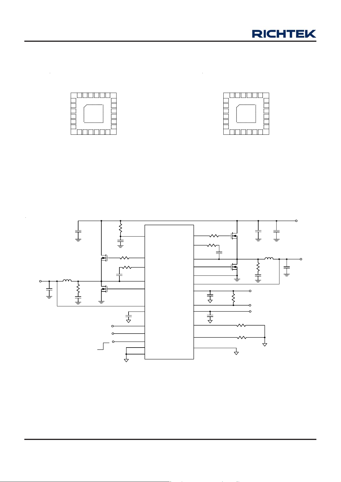
Typical Application Circuit
For Fixed V oltage Regulator
C
1
µ
F
0
1
Q1
BSC119
N03S
1
L
H
8
6
µ
V
O
U
T
1
V
5
3
C
F
µ
2
0
2
.
R
5
BSC119
C
N03S
4
u
e
e
q
r
F
E
M
D
/
M
W
P
0
Q3
n
r
t
y
C
n
o
c
o
n
s
r
t
a
U
l
/
ON
OFF
R
3
4
R
R
3
C
2
F
µ
.
1
C
1
1
F
2
2
.
µ
0
l
o
c
i
VOUT2
VREG3
BOOT2
LGATE2
PHASE2
UGATE2
RT8223B
WQFN-24L 4x4
V
I
7
.
9
16
C
6
F
1
µ
.
0
0
21
0
22
20
19
24
3
4
14
13
2
5
VIN
UGATE1
BOOT1
PHASE1
LGATE1
VOUT1
REF
TONSEL
SKIPSEL
EN
FB1
FB2
RT8223A
UGATE2
BOOT2
PHASE2
LGATE2
PGND
VOUT2
VREG5
PGOOD
VREG3
ENTRIP1
ENTRIP2
GND
R
9
10
9
11
12
15
7
17
23
8
1
6
Exposed Pad (25)
0
0
8
R
C
5
4
.
µ
7
C
1
2
4
.
7
µ
Q2
BSC119
N03S
7
C
.
0
µ
1
F
Q4
BSC119
N03S
R
6
F
F
0
0
1
k
1
R
5
1
k
0
2
R
1
5
0
k
9
C
1
4
R
C
5
V
l
A
w
O
O
G
P
3
.
V
3
A
C
µ
0
L
.
1
0
1
a
D
l
w
8
F
1
µ
0
2
7
µ
H
0
y
n
s
O
I
d
n
i
c
a
o
t
r
a
y
s
O
n
N
F
V
U
O
2
T
.
3
3
C
2
V
3
1
0
2
µ
F
DS8223A/B-04 April 2011www.richtek.com
2
RT8223A/B
V
I
R
C
µ
OFF
OFF
y
t
l
7
9
3
.
16
0
C
1
1
0
.
µ
F
R
0
4
R
2
F
ON
ON
o
r
t
C
o
n
s
o
a
n
i
r
21
0
3
22
20
19
24
18
3
5
C
1
F
.
2
0
2
µ
13
l
c
4
14
C
1
F
0
u
1
Q1
BSC119
N03S
L
1
8
µ
H
6
V
1
O
U
T
5
V
3
C
F
2
2
0
µ
.
R
5
BSC119
C
N03S
4
P
W
1
0
.
Q3
n
c
e
F
r
e
q
u
U
/
M
/
M
D
E
VIN
UGATE1
BOOT1
PHASE1
LGATE1
VOUT1
ENC
REF
EN
TONSEL
SKIPSEL
RT8223B
UGATE2
BOOT2
PHASE2
LGATE2
PGND
VOUT2
VREG5
PGOOD
VREG3
ENTRIP1
ENTRIP2
FB1
FB2
GND
10
9
11
12
15
7
17
23
8
1
6
2
5
Exposed Pad (25)
9
R
0
8
R
0
C
9
.
µ
4
7
1
C
6
.
4
µ
7
Q2
BSC119
N03S
7
C
.
0
1
F
µ
Q4
BSC119
N03S
6
R
F
1
k
0
0
F
1
R
0
5
1
k
2
R
5
1
0
k
C
3
1
1
µ
0
L
.
4
7
1
R
0
C
1
5
V
A
l
a
w
P
D
O
O
G
3
A
.
V
3
l
w
1
C
F
1
0
2
µ
H
4
y
s
On
n
c
I
i
d
r
a
o
t
a
y
s
On
N
2
F
µ
V
U
T
2
O
.
V
3
3
1
C
7
2
µ
0
F
2
DS8223A/B-04 April 2011 www.richtek.com
3
RT8223A/B
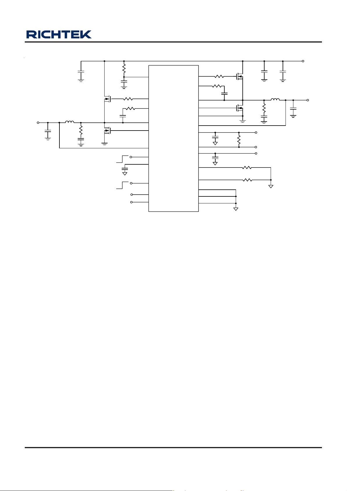
For Adjustable V oltage Regulator
C
1
µ
F
0
1
Q1
BSC119
N03S
1
L
H
6
8
.
V
O
T
U
1
V
5
3
C
F
µ
2
0
2
1
C
1
5
C
F
1
.
µ
0
µ
e
r
M
/
BSC119
N03S
q
e
n
u
E
M
D
Q3
y
C
c
o
r
t
s
l
a
U
/
R
5
C
4
4
1
1
R
k
5
1
2
R
1
k
0
1
F
W
P
OFF
n
o
0
t
n
ON
V
I
R
7
.
3
9
16
C
6
1
.
F
µ
0
0
4
R
R
C
2
.
F
µ
1
21
0
3
22
20
19
24
VIN
UGATE1
BOOT1
PHASE1
LGATE1
VOUT1
RT8223A
UGATE2
BOOT2
PHASE2
LGATE2
PGND
VOUT2
FB2
ENTRIP1
ENTRIP2
2
FB1
3
4
14
13
REF
TONSEL
SKIPSEL
EN
1
1
C
2
F
µ
.
0
2
r
l
o
c
i
GND
VREG5
PGOOD
VREG3
R
9
10
9
0
8
0
R
11
12
15
7
5
1
R
k
5
1
1
6
0
2
R
k
0
1
5
Exposed Pad (25)
17
5
C
4
.
7
µ
23
8
2
1
C
4
.
7
µ
Q2
BSC119
N03S
7
C
µ
.
1
0
F
Q4
BSC119
N03S
R
6
F
1
0
0
k
F
9
C
1
4
R
1
C
V
5
l
w
A
O
G
P
O
.
3
3
V
A
C
µ
0
L
.
8
F
µ
1
0
2
7
H
µ
0
1
0
R
1
.
6
R
1
1
0
a
s
y
n
O
D
I
n
d
i
c
a
t
o
r
l
a
w
s
y
n
O
N
F
V
U
O
2
T
3
.
V
3
C
3
1
0
2
µ
F
2
1
7
C
3
5
k
4
k
6
C
1
F
1
.
µ
0
V
I
R
C
1
F
0
µ
1
Q1
BSC119
N03S
L
1
8
H
µ
6
V
T
1
O
U
5
V
3
C
F
2
0
µ
2
.
R
5
BSC119
C
N03S
4
Q3
1
0
.
7
9
.
3
16
0
C
1
1
F
µ
.
0
R
0
4
21
0
R
3
22
C
2
µ
F
20
19
24
8
C
1
R
1
1
5
k
1
C
1
9
R
1
1
µ
.
F
0
2
0
k
1
ON
OFF
ON
2
18
3
C
1
5
F
µ
2
2
0
.
13
OFF
o
l
r
t
y
C
o
n
c
u
e
n
q
F
e
r
o
c
n
s
i
/
r
t
U
a
l
D
/
E
M
P
M
W
4
14
VIN
UGATE1
BOOT1
PHASE1
LGATE1
VOUT1
FB1
ENC
REF
EN
TONSEL
SKIPSEL
RT8223B
UGATE2
BOOT2
PHASE2
LGATE2
PGND
VOUT2
FB2
ENTRIP1
ENTRIP2
GND
VREG5
PGOOD
VREG3
10
9
11
12
15
7
5
1
6
Exposed Pad (25)
17
23
8
9
R
0
0
8
R
Q2
BSC119
N03S
7
C
.
µ
F
0
1
Q4
BSC119
N03S
1
R
1
0
5
k
2
R
0
5
1
k
C
9
.
4
7
µ
1
C
6
.
4
7
µ
6
R
F
0
1
0
k
F
C
3
1
0
1
µ
L
4
7
.
1
R
0
C
1
4
V
5
l
a
A
w
P
O
O
G
D
.
3
V
3
l
A
w
1
C
F
1
µ
0
2
µ
H
R
1
6
.
R
1
1
0
y
n
s
O
I
d
n
i
c
t
a
r
o
y
a
n
s
O
N
2
F
V
O
U
2
T
.
3
3
V
7
1
C
2
F
2
µ
0
1
2
C
3
5
k
4
k
0
2
C
F
µ
.
1
0
DS8223A/B-04 April 2011www.richtek.com
4
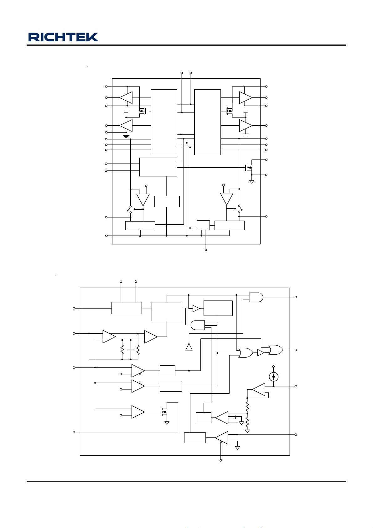
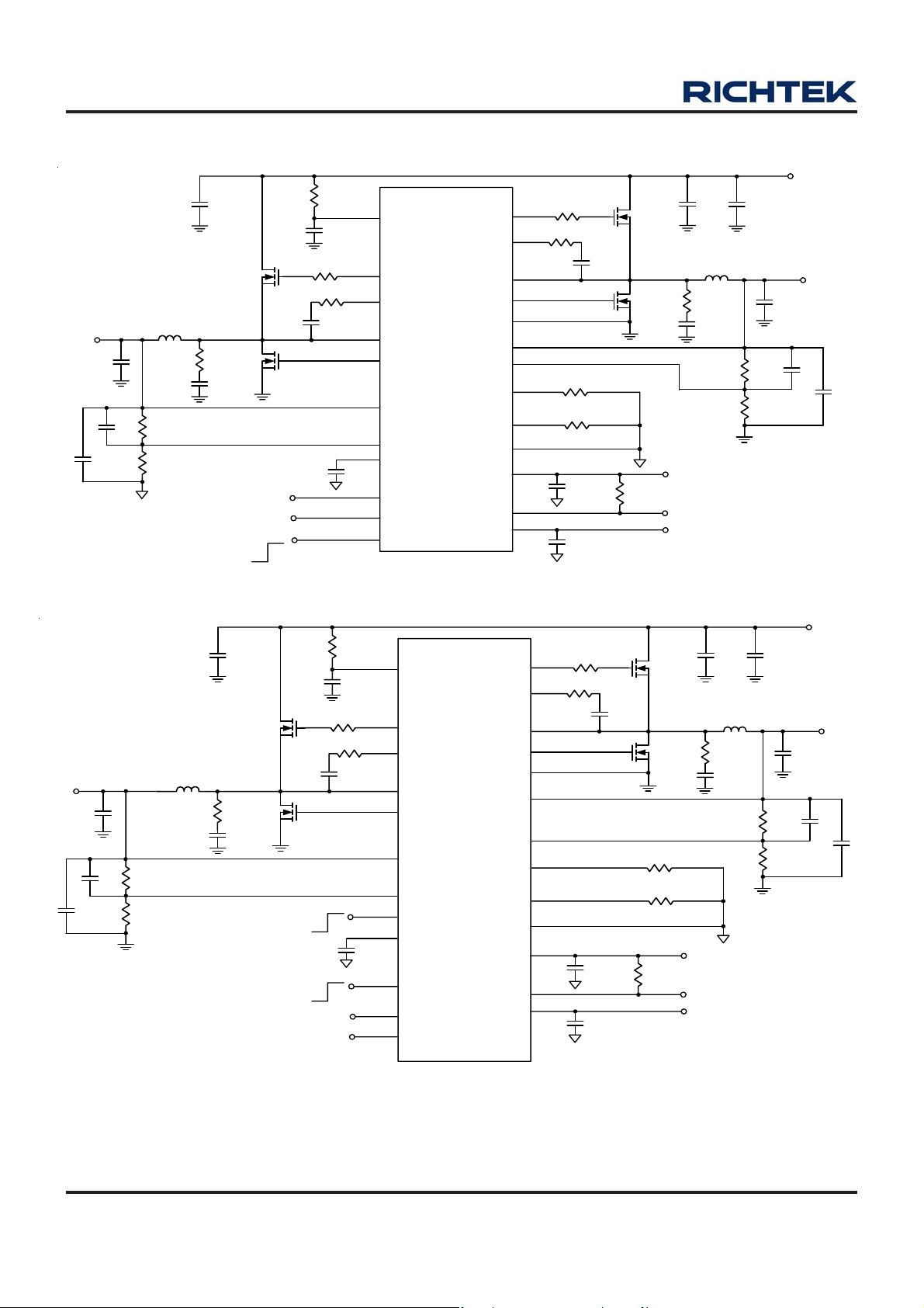
Function Block Diagram
RT8223A/B
TONSEL SKIPSEL
BOOT1
UGATE1
PHASE1
LGATE1
PGND
VOUT1
FB1
ENTRIP1
EN
ENC
VREG5
VIN
VREG5
PWM Buck
Power-On
Sequence
Clear Fault Latch
SW Threshold
VREG5
SMPS1
Controller
Thermal
Shutdown
SMPS2
PWM Buck
Controller
SW Threshold
REF
REF
Function Block Di agra m
VREG3
VREG5
BOOT2
UGATE2
PHASE2
LGATE2
VOUT2
FB2
ENTRIP2
PGOOD
GND
VREG3
VOUT
REF
FB
PGOOD
+
1.1 x V
0.6 x V
0.9 x V
+
-
REF
REF
REF
On-Time
Compute
VINTONSEL
+
Over-Voltage
+
-
+
Under-Voltage
+
T
ON
Comp
Q
1-Shot
TRIG
Fault
Latch
Blanking
Time
R
25kHz
Detector
TRIG
SS
Time
Detector
Zero
T
1-Shot
Q
S
OFF
Current
+
-
+
+
-
Limit
VREG5
+
-
UGATE
LGATE
ENTRIP
PHASE
SKIPSEL
PWM Controller (One Side)
DS8223A/B-04 April 2011 www.richtek.com
5

RT8223A/B
Functional Pin Description
ENTRIP1 (Pin 1)
Channel 1 enable a nd Current Limit setting Input. Connect
a resistor to GND to set the threshold for channel 1
synchronous R
limit threshold is 1/10th the voltage seen at ENTRIP1 over
a 0.5V to 2V range. There is an internal 10μA current
source from VREG5 to ENTRIP1.
FB1 (Pin 2)
SMPS1 Feedback Input. Connect FB1 to VREG5 or GND
for fixed 5V operation. Or connect FB1 to a resistive voltagedivider from VOUT1 to GND to adjust output from 2V to
5.5V.
REF (Pin 3)
2V Reference Output. Bypass to GND with a 0.22μF
cap acitor . REF ca n source up to 50μA f or external loads.
Loading REF degrades FBx and output a ccuracy a ccording
to the REF load regulation error.
TONSEL (Pin 4)
Frequency Selectable Input for VOUT1/VOUT2
respectively .
400kHz/500kHz : Connect to VREG5 or VREG3
300kHz/375kHz : Connect to REF
200kHz/250kHz : Connect to GND
FB2 (Pin 5)
SMPS2 Feedback Input. Connect FB2 to VREG5 or GND
for fixed 3.3V operation. Or connect FB2 to a resistive
voltage-divider from VOUT2 to G ND to adjust output from
2V to 5.5V.
ENTRIP2 (Pin 6)
Channel 2 enable a nd Current Limit setting Input. Connect
a resistor to GND to set the threshold for channel 2
synchronous R
limit threshold is 1/10th the voltage seen at ENTRIP2 over
a 0.5V to 2V range. There is an internal 10μA current
source from VREG5 to ENTRIP2.
sense. The GND − PHASE1 current-
DS(ON)
sense. The GND − PHASE2 current
DS(ON)
VOUT2 (Pin 7)
SMPS2 Output Voltage Sense Input. Connect to the
SMPS2 output. VOUT2 is an input to the on-time one
shot circuit. It also serves as the SMPS2 feedback input
in fixed voltage mode.
VREG3 (Pin 8)
3.3V Linear Regulator Output.
BOOT2 (Pin 9)
Boost Flying Cap acitor Conne ction for SMPS2. Connect
to an external ca pa citor according to the typical a pplication
circuits.
UGA TE2 (Pin 10)
High-Side MOSFET Floating Gate Driver Output for
SMPS2. UGA TE2 swings between PHASE2 and BOOT2.
PHASE2 (Pin 11)
Inductor Connection for SMPS2. PHASE2 is the internal
lower supply rail for the UGATE2 high side gate driver.
PHASE2 is also the current-sense input for the SMPS2.
LGA TE2 (Pin 12)
SMPS2 Synchronous-Rectifier Gate-Drive Output.
LGA TE2 swings between PGND a nd VREG5.
EN (Pin 13)
Master Enable Input. The REF/VREG5/VREG3 are
enabled if it is within logic high level and disabled if it is
less than the logic low level.
SKIPSEL (Pin 14)
Operation Mode Selectable Input.
Ultrasonic Mode : Connect to VREG5 or VREG3
Diode Emulation Mode : Connect to GN D
PWM Mode : Connect to REF
GND [Exposed Pad (25)]
Analog Ground for SMPS controller. The exposed pad
must be soldered to a large PCB and connected to GND
for maximum power dissipation.
DS8223A/B-04 April 2011www.richtek.com
6

RT8223A/B
PGND (Pin 15)
Power Ground for SMPS controller. Connect PGND
externally to the underside of the exposed pad.
VIN (Pin 16)
High Voltage Power Supply Input for 5V/3.3V LDO and
Feed-forward ON-Ti me circuitry .
VREG5 (Pin 17)
5V Linear Regulator Output.VREG5 is also the supply
voltage for the low-side MOSFET driver a nd analog supply
voltage for the device.
NC (Pin 18) (RT8223A)
No Internal Connection.
ENC (Pin 18) (RT8223B)
SMPSx Enable Input. Pull up to VREG3 or VREG5 to
turn on both switcher channels. Short to GND to shutdown
them.
VOUT1 (Pin 24)
SMPS1 Output Voltage-Sense Input. Connect to the
SMPS1 output. VOUT1 is an input to the on-time one
shot circuit. It also serves as the SMPS1 feedback input
in fixed-voltage mode.
LGA TE1 (Pin 19)
SMPS1 Synchronous Rectifier Gate Drive Output. LGA TE1
swings between PGND a nd VREG5.
PHASE1 (Pin 20)
Inductor Connection for SMPS1. PHASE1 is the internal
lower supply rail for the UGATE1 high side gate driver.
PHASE1 is also the current sense input for the SMPS1.
UGA TE1 (Pin 21)
High-Side MOSFET Floating Gate Driver Output for
SMPS1. UGA TE1 swings between PHASE1 and BOOT1.
BOOT1 (Pin 22)
Boost Flying Cap acitor Conne ction for SMPS1. Connect
to an external ca pa citor according to the typical a pplication
circuits.
PGOOD (Pin 23)
Power Good Output f or channel 1 a nd channel 2. (Logical
AND)
DS8223A/B-04 April 2011 www.richtek.com
7

RT8223A/B
Absolute Maximum Ratings (Note 1)
z VIN, EN to GND-------------------------------------------------------------------------------------------------------------- –0.3V to 30V
z PHASEx to GND
DC------------------------------------------------------------------------------------------------------------------------------- –0.3V to 30V
< 20ns ------------------------------------------------------------------------------------------------------------------------- −8V to 38V
z BOOTx to PHASEx--------------------------------------------------------------------------------------------------------- –0.3V to 6V
z ENTRIPx, SKIPSEL, TONSEL, PGOOD, to GND------------------------------------------------------------------- –0.3V to 6V
z VREG5, VREG3, FBx, VOUTx, ENC, REF to GND ---------------------------------------------------------------- –0.3V to 6V
z UGATEx to PHASEx
DC------------------------------------------------------------------------------------------------------------------------------- –0.3V to 6V
< 20ns ------------------------------------------------------------------------------------------------------------------------- −5V to 7.5V
z LGATEx to GND
DC------------------------------------------------------------------------------------------------------------------------------- –0.3V to 6V
< 20ns ------------------------------------------------------------------------------------------------------------------------- −2.5V to 7.5V
z Power Dissipation, P
WQFN-24L 4x4 -------------------------------------------------------------------------------------------------------------- 1.923W
z Package Thermal Re sistance (Note 2)
WQF N-24L 4x4, θJA--------------------------------------------------------------------------------------------------------- 52°C/W
WQFN-24L 4x4, θJC-------------------------------------------------------------------------------------------------------- 7°C/W
z Lead T e mperature (Soldering, 10 sec.)--------------------------------------------------------------------------------- 2 60 °C
z Junction T emperature------------------------------------------------------------------------------------------------------- 150°C
z Storage T emperature Range ---------------------------------------------------------------------------------------------- –65°C to 150°C
z ESD Susceptibility (Note 3)
HBM (Human Body Mode) ------------------------------------------------------------------------------------------------ 2kV
MM (Ma chine Mode)-------------------------------------------------------------------------------------------------------- 200V
@ TA = 25°C
D
Recommended Operating Conditions (Note 4)
z Input Voltage, V
z Junction T emperature Range---------------------------------------------------------------------------------------------- −40°C to 125°C
z Ambient T emperature Range---------------------------------------------------------------------------------------------- −40°C to 100°C
8
------------------------------------------------------------------------------------------------------------ 6V to 25V
IN
DS8223A/B-04 April 2011www.richtek.com
RT8223A/B
Electrical Characteristics
(VIN = 12V, EN = ENC = 5V, ENTRIP1 = ENTRIP2 = 2V, No Load on VREG5, VREG3, VOUT1, VOUT2 and REF , T
unless otherwise specified)
Parameter Symbol Test Conditions Min Typ Max Unit
Input Supply
VIN Standby Supply
Current
VIN Shutdown Supply
Current
Quiescent Power
Cons umption
I
VIN_SBY
I
VIN_S HDH
SMPS Output and FB Voltage
VOUT1 Output Voltage in
Fixed Mode
VOUT2 Output Voltage in
Fixed Mode
FBx in Output Adjustable
Mode
Output Voltage
Adjustment Range
FBx A djustab le -mode
Threshold Voltage
Line Regulation V
V
OUT1
V
OUT2
FBx V
V
OUT x
Fixed or Adj-Mode comparator threshold 0.2 0.4 0.55 V
LOAD
LINE
On Time
SMPS1, SMPS2 2 -- 5.5 V
Either SMPS, VIN = 6V to 25V -- 0.005 -- %/V
= 6V to 2 5 V, Both SMP S Off,
V
IN
EN = 5V, ENC = GND
-- 200 -- μA
VIN = 6V to 25V, ENTRIPx = EN = GND -- 20 40 μA
Bot h SMPSs O n, FBx = SKIPSEL = R E F
V
= 5.3V, V
OUT1
V
= 6V to 25V, FB1= REF or 5V,
IN
= 3.5V (Note 5)
OUT2
SK IPSEL = REF
= 6V to 25V, FB2 = REF or 5V,
V
IN
SK IPSEL = REF
= 6V to 25V 1.975 2 2.025 V
IN
-- 5 7 mW
4.975 5.05 5.125 V
3.285 3.33 3.375 V
Either SMPS, SKIPSEL = REF, 0 to 5A -- −0.1 -Either SMPS, SKIPSEL = VREG5, 0 to 5A -- −1.7 -- DC Load Regulation V
Either SMPS, SKIPSEL = GND, 0 to 5A -- −1.5 --
= 25°C,
A
%
On-Time Pulse Width t
Mini mum Off-T i me t
Ultrasonic Mode
Frequency
Soft Start
Sof t-Start Ti me t
Current Sense
Current Limit Threshold
(Default)
ENTRIPx Source Current I
ENTRIPx Current
Temperature Coefficient
ENTRIPx Adjustment
Range
V
= 5.05V 1895 2105 2315
TONSEL = GND
TONSEL = REF
UGATEx
TONSEL = VREG5
200 300 400 ns
LGATEx
OUT1
= 3.33V 999 1110 1221
V
OUT2
V
= 5.05V 1227 1403 1579
OUT1
= 3.33V 647 740 833
V
OUT2
V
= 5.05V 895 1052 1209
OUT1
V
= 3.33V 475 555 635
OUT2
ns
SKIPSEL = VREG5 or VREG3 20 28 -- kHz
Zero to Full Limit from ENTR IPx Enable -- 2 -- ms
SSx
V
ENTRIPx
TC
IENTRIPx
V
ENTRIPx
V
ENTRIPx
-- 1600 -- PPM/°C
ENTRIPx
= VREG 5, GN D−PHASEx 180 200 220 mV
= 0.9V 9.4 10 10.6 μA
= I
ENTRIPx
x R
ENTRIPx
0.5 -- 2 V
To be continued
DS8223A/B-04 April 2011 www.richtek.com
9

RT8223A/B
Parameter Symbol Test Conditions Min Typ Max Unit
Current Limit Threshold GND−PHASEx, V
Zero-Current Threshold
SKIPSEL = VREG5 or GND,
GND−PHASEx
ENTRIPx
=2V 180 200 220 m V
-- 3 -- mV
Internal Regula tor and Re fer e nce
= GND, 6V < VIN < 25V,
V
VREG5 Output Voltage V
VREG3 Output Voltage V
VREG5 Short Current I
VREG3 Short Current I
VREG5 Switchover Threshold
OUT1
to V
VREG3 Switchover Threshold V
VREGx Switchover Equivalent
Resistance
REF Output V oltage V
VREG5
VREG3
VREG5 = GND, V
VREG5
VREG3 = GND, V
VREG3
SW3
VREGx to V
R
SW
No External Load 1.98 2 2.02 V
REF
OUT1
0 < I
V
OUT2
0 < I
Rising Edge at V
Point
Rising Edge at V
Point, Hysteresis = 6%
REF Load Regu la t ion 0 < I
< 70mA
VREG5
= GND, 6V < VIN < 25V,
< 70mA
VREG3
= GND -- 175 275 mA
OUT1
= GND -- 175 275 mA
OUT2
Regulation
OUT1
Regulation
OUT2
, 10mA -- 1. 5 3 Ω
OUTx
< 50uA -- 10 -- mV
LOAD
4.8 5 5.2 V
3.2 3.33 3.46 V
4.53 4.66 4.79 V
2.98 3.08 3.18 V
REF Sink Current REF in Regulation 5 -- -- μA
UVLO
VREG3 UVLO Threshold SMPSx off -- 2.5 -- V
VREG5 UVLO Threshold
Rising Edge -- 4.35 4.5 V
Falling Edge 3.9 4.05 4.25 V
Power Good
PGOOD Threshold V
PGOODx
PGOOD Detect (FBx Rising Edge) −11 −7.5 −4
%
Hysteresis -- 8 -PGOOD Propagation Delay Falling Edge, 50mV Overdrive -- 10 -- μs
PGOOD Leakage Current High State, Forced to 5.5V -- -- 1 μA
PGOOD Output Low Voltag e I
= 4mA -- -- 0.3 V
SINK
Fault Detection
OVP Trip Threshold V
FB_OVP
FBx with Respect to Internal
Reference
108 111 115 %
OVP Propagation Delay -- 10 -- μs
UVP Trip Threshold VUV
UVP Detect (FBx Falling Edge) 46 52 58
%
Hysteresis -- 8 -UVP Shutd ow n Blanki ng Time t
SHDN_UVP
From ENTRIPx Enable -- 3 -- ms
Thermal Shutdown
Thermal Shutdown T
Thermal Shutdown Hysteresis
-- 150 -- °C
SHDN
-- 10 -- °C
Discharge
VO UTx Discharge Current I
ENTRI Px = ENC = 0V, V
DISx
= 0.5V 10 60 -- mA
OUTx
VREGx Discharge Current EN = 0V , VREGx = 0.5V 2.5 -- -- mA
10
To be continued
DS8223A/B-04 April 2011www.richtek.com

RT8223A/B
Parameter Symbol Test Conditions Min Typ Max Unit
Logic Input
FB1/FB2 Input Voltage
SKIPSEL Input Voltage
ENTRIPx Input Voltage V
ENTRIPx
EN Current IEN
ENC Threshold Voltage
(RT8223B)
V
ENC
Inpu t Leakage Cu rren t
Internal BOOT Switch
Internal Boost Charging
Switch On-Resistance
Po we r MO SF E T Drivers
UGATEx On-Resistance
LGAT Ex On-Resistance
Dead Time
Note 1. Stresses listed as the above "Absolute Maximum Ratings" may cause permanent damage to the device. These are for
stress ratings. Functional operation of the device at these or any other conditions beyond those indicated in the
operational sections of the specifications is not implied. Exposure to absolute maximum rating conditions for extended
periods may remain possibility to affect device reliability.
Note 2. θ
Note 3. Devices are ESD sensitive. Handling precaution is recommended.
Note 4. The device is not guaranteed to function outside its operating conditions.
Note 5. P
is measured in natural convection at TA = 25°C on a high effective thermal conductivity four-layer test board of
JA
JEDEC 51-7 thermal measurement standard. The measurement case positions of θ
package and the expose pad for the SOP(Exposed Pad) package.
+ P
VIN
VREG5
UGATEx, High state -- 3 6
UGATEx, Low state -- 1.5 4
LGATEx, High State -- 2.2 5
LGATEx, Low State -- 0. 6 1.5
LGATEx Rising -- 30 --
Low Level (Internal Fixed VOUTx) -- -- 0.2
High Level (Internal Fixed VOUTx) 4.5 -- --
V
Low Level (DEM Mode) -- -- 0.8
REF Level (P WM Mode) 1.8 -- 2.3
V
High Level (Ultrasonic Mode) 2.7 -- -Low Level (SMPSs Off) -- -- 0.35
On Level (SMPSs On) 0.5 -- 2
V
High Level (SMPSs Off) 4.5 -- -Shutdown -- -- 0.4
Enable 2.4 -- -- EN Voltage VEN
V
Open 2.4 3.3 4.2
V
= 0.2V (Source) 1 3 5
EN
= 3.3V (Sink) -- 3 8
V
EN
Shutdown
Enable
V
OUT1/VOUT2
V
OUT1/VOUT2
V
OUT1/VOUT2
= 200kHz/250kHz -- -- 0.8
= 300kHz/375kHz 1.8 -- 2.3 TONSEL Setting Voltage
= 400kHz/500kHz 2.7 -- --
-- -- 0.6
2 -- --
TONSEL, SKIPSEL = 0V or 5 V −1 -- 1
ENC = 0V or 5V (RT8223B ) −1 -- 1
μA
V
V
μA
V REG5 to BO OTx -- 20 -- Ω
Ω
UGATEx Rising -- 40 --
are on the lead of the SOP
JC
ns
DS8223A/B-04 April 2011 www.richtek.com
11

RT8223A/B
Typical Operating Characteristics
V
Output Efficiency vs. Load Current
OUT1
100
90
DEM Mode
80
70
60
50
40
Eff iciency (%)
30
20
10
0
0.001 0.01 0.1 1 10
PWM Mode
VIN = 8V , T ONSEL = GND, EN = VIN,
ENTRIP1 = 0.91V , ENTRIP2 = GND
Load Curr ent ( A )
V
Output Effic iency vs. Load Current
OUT1
100
90
80
DEM Mode
70
60
50
40
Eff iciency (%)
30
20
10
0
0.001 0.01 0.1 1 10
VIN = 12V , T ONSEL = GND, EN = VIN,
ENTRIP1 = 0.91V , ENTRIP2 = GND
Load Current (A)
Ultrasonic Mode
Ultrasonic Mode
PWM Mode
V
Output Efficiency v s . Loa d Current
OUT2
100
90
80
DEM Mode
70
60
50
40
Efficiency (%)
30
20
10
0
0.001 0.01 0.1 1 10
VIN = 8V , T ONSEL = GND, EN = VIN,
ENTRIP1 = GND, ENTRIP2 = 0.91V
Ultrasonic Mode
PWM Mode
Load Current (A)
V
Output Efficiency vs. Load Current
OUT2
100
90
80
70
60
50
40
Efficiency (%)
30
20
10
0
0.001 0.01 0.1 1 10
DEM Mode
Ultrasonic Mode
PWM Mode
VIN = 12V , T ONSEL = GND, EN = VIN,
ENTRIP1 = GND, ENTRIP2 = 0.91V ,
Load Current (A)
12
V
Output Effic iency vs. Load Current
OUT1
100
90
80
DEM Mode
70
60
50
40
Eff iciency (%)
30
20
10
0
0.001 0.01 0.1 1 10
VIN = 20V , T ONSEL = GND, EN = VIN,
ENTRIP1 = 0.91V , ENTRIP2 = GND
Ultrasonic Mode
PWM Mode
Load Curr ent ( A )
V
Output Efficiency vs. Load Current
OUT2
100
90
80
70
60
50
40
Efficiency (%)
30
20
10
0
0.001 0.01 0.1 1 10
DEM Mode
Ultrasonic Mode
PWM Mode
VIN = 20V
TONSEL = GND, EN = VIN,
ENTRIP1 = GND, ENTRIP2 = 0.91V
Load Current (A)
DS8223A/B-04 April 2011www.richtek.com

V
Output Switching Frequency v s . Load Current
OUT1
250
VIN = 8V , T ONSEL = GND, EN = VIN,
225
ENTRIP1 = 0.91V , ENTRIP2 = GND
200
175
150
125
100
75
50
Switching Frequency (kHz)
25
0
0.001 0.01 0.1 1 10
PWM Mode
Ultrasonic Mode
DEM Mode
Load Current (A)
V
Output Switching Frequency vs. Load Current
OUT1
250
VIN = 12V , T ONSEL = GND, EN = VIN,
225
ENTRIP1 = 0.91V , ENTRIP2 = GND
200
175
150
125
100
75
50
Swit ching Frequency (kH z)
25
0
0.001 0.01 0.1 1 10
PWM Mode
Ultrasonic Mode
DEM Mode
Load Current (A)
RT8223A/B
V
Output Switching Frequency v s . Loa d Current
OUT2
300
VIN = 8V , T ONSEL = GND, EN = VIN,
275
ENTRIP1 = GND, ENTRIP2 = 0.91V
250
225
200
175
150
125
100
75
50
Swit ching Frequency ( kHz)
25
0
V
Output Switching Frequency v s . Loa d Current
OUT2
300
275
250
225
200
175
150
125
100
75
50
Swit ching Frequency (kH z)
25
PWM Mode
Ultrasonic Mode
DEM Mode
0.001 0.01 0.1 1 10
Load Current (A)
VIN = 12V , TONSEL = GND, EN = VIN,
ENTRIP1 = GND, ENTRIP2 = 0.91V
PWM Mode
Ultrasonic Mode
0
0.001 0.01 0.1 1 10
DEM Mode
Load Curr ent (A )
V
V
Output Switching Frequency vs. Load Current
OUT1
250
VIN = 20V , T ONSEL = GND, EN = VIN,
225
ENTRIP1 = 0.91V , ENTRIP2 = GND
200
175
150
125
100
75
50
Switching Frequency (kHz)
25
0
0.001 0.01 0.1 1 10
PWM Mode
Ultrasonic Mode
DEM Mode
Load Current (A)
Output Switching Frequency v s . Load Current
OUT2
300
VIN = 20V , T ONSEL = GND, EN = VIN,
275
ENTRIP1 = GND, ENTRIP2 = 0.91V
250
225
200
175
150
125
100
75
50
Switching Frequency (kHz)
25
0
PWM Mode
Ultrasonic Mode
DEM Mode
0.001 0.01 0.1 1 10
Load Current (A)
DS8223A/B-04 April 2011 www.richtek.com
13

RT8223A/B
V
Output Voltage vs. Load Current
OUT1
Output Voltage (V)
5.114
5.108
5.102
5.096
5.090
5.084
5.078
5.072
5.066
5.060
5.054
5.048
VIN = 12V , TONSEL = GND, EN = VIN,
ENTRIP1 = 0.91V , ENTRIP2 = GND
Ultrasonic Mode
DEM Mode
PWM Mode
0.001 0.01 0.1 1 10
Load Curr ent ( A)
V
Output Voltage vs. Load Current
OUT2
VIN = 12V , T ONSEL = GND, EN = VIN,
ENTRIP1 = GND, ENTRIP2 = 0.91V
Ultrasonic Mode
DEM Mode
PWM Mode
0.001 0.01 0.1 1 10
Output V oltage (V)
3.378
3.372
3.366
3.360
3.354
3.348
3.342
3.336
3.330
3.324
Load Current (A)
Output Voltage (V)
2.0030
2.0028
2.0026
2.0024
2.0022
(V)
2.0020
REF
2.0018
V
2.0016
2.0014
2.0012
2.0010
VREG5 Output Voltage vs. Output Current
4.980
VIN = 12V , T ONSEL = GND, EN = VIN,
4.978
ENTRIP1 = ENTRIP2 = GND
4.976
4.974
4.972
4.970
4.968
4.966
4.964
4.962
4.960
0 10203040506070
Output Current (mA)
V
vs. Output Current
REF
VIN = 12V , T ONSEL = GND, EN = VIN,
ENTRIP1 = ENTRIP2 = GND
-10 0 10 20 30 40 50
Output Current (uA)
VREG3 Output Voltage vs. Output Current
3.324
VIN = 12V , T ONSEL = GND, EN = VIN,
ENTRIP1 = ENTRIP2 = GND
3.322
3.320
3.318
3.316
3.314
3.312
Output Voltage ( V)
3.310
3.308
3.306
0 10203040506070
Output Current (mA)
Battery Current vs. Input Voltag e
100
PWM Mode
10
Ultrasonic Mode
1
Battery Current (mA)
0.1
DEM Mode
No Load, TONSEL = GND, EN = VIN,
ENTRIP1 = ENTRIP2 = 0.91V
7 9 11 13 15 17 19 21 23 25
Inpu t Voltage (V)
14
DS8223A/B-04 April 2011www.richtek.com

RT8223A/B
(V)
REF
V
Standby Input Current vs. Input Voltage
252
No Load, EN = VIN, ENTRIP1 = ENTRIP2 = GND
250
248
246
244
242
Standby I nput Current (uA)
240
7 9 11 13 15 17 19 21 23 25
Input Vol tage (V)
V
vs. Temperature
2.011
2.008
2.005
2.002
1.999
1.996
REF
22
20
18
16
14
12
10
Shutdown I nput Curr ent (uA)
VREG5
(5V/Div)
VREG3
(5V/Div)
REF
(5V/Div)
Shutdown Input Current v s . Input Voltage
No Load, EN = GND, ENTRIP1 = ENTRIP2 = GN D
8
7 9 11 13 15 17 19 21 23 25
Inpu t Voltage (V)
Start Up
1.993
1.990
V
OUT1
(5V/Div)
Inductor
Current
(2A/Div)
ENTRIP1
(2V/Div)
PGOOD
(10V/Div)
VIN = 12V , ENTRIP1 = ENTRIP2 = GND,
EN = V
-50 -25 0 25 50 75 100 125
, TONSEL = GND
IN
Temperature
V
Start Up
OUT1
No Load, VIN = 12V , T ONSEL = GND, EN = V
ENTRIP1 = ENTRIP2 = 0.91V
(°C)
IN
Time (400μs/Div)
EN
(10V/Div)
V
OUT1
(5V/Div)
Inductor
Current
(2A/Div)
ENTRIP1
(2V/Div)
PGOOD
(10V/Div)
No Load, VIN = 12V , T ONSEL = GND,
, ENTRIP1 = ENTRIP2 = GND
EN = V
IN
Time (400μs/Div)
V
Start Up
OUT1
Heavy Load, VIN = 12V, TONSEL = GND, EN = V
ENTRIP1 = NTRIP2 = 0.91V , I
OUT1
= 4A
Time (400μs/Div)
IN
DS8223A/B-04 April 2011 www.richtek.com
15

RT8223A/B
No Load, VIN = 12V , T ONSEL = GND, EN = V
V
OUT2
(5V/Div)
Inductor
Current
(2A/Div)
ENTRIP2
(2V/Div)
PGOOD
(10V/Div)
ENTRIP1 = ENTRIP2 = 0.91V
V
OUT2
Start Up
V
Start Up
OUT2
IN
V
OUT2
Heavy Load, VIN = 12V, TONSEL = GND, EN = V
IN
(5V/Div)
Inductor
Current
(2A/Div)
ENTRIP2
(2V/Div)
PGOOD
(10V/Div)
ENTRIP1 = ENTRIP2 = 0.91V
V
OUT1
(5V/Div)
V
OUT2
(5V/Div)
ENTRIP1
(1V/Div)
ENTRIP2
(1V/Div)
V
OUT1
V
OUT1_ac
(50mV/Div)
Time (400μs/Div)
V
Delay Start
OUT1
No Load, VIN = 12V , T ONSEL = GND, EN = V
IN
Time (400μs/Div)
PWM Mode Load Transient Response
VIN = 12V , T ONSEL = GND, EN = VIN,
SKIPSEL = GND, I
OUT1
= 0A to 6A
V
OUT1
(5V/Div)
V
OUT2
(5V/Div)
ENTRIP1
(1V/Div)
ENTRIP2
(1V/Div)
V
OUT2
V
OUT2_ac
(50mV/Div)
Time (400μs/Div)
V
Delay Start
OUT2
No Load, VIN = 12V , T ONSEL = GND, EN = V
IN
Time (400μs/Div)
PWM Mode Load Transient Response
VIN = 12V , T ONSEL = GND, EN = VIN,
SKIPSEL = GND, I
= 0A to 6A
OUT2
Inductor
Current
(5A/Div)
UGATE1
(20V/Div)
LGATE1
(10V/Div)
16
Time (20μs/Div)
Inductor
Current
(5A/Div)
UGATE2
(20V/Div)
LGATE2
(10V/Div)
Time (20μs/Div)
DS8223A/B-04 April 2011www.richtek.com

RT8223A/B
V
OUT1
(5V/Div)
UGATE1
(20V/Div)
LGATE1
(5V/Div)
ENTRIP1
(1V/Div)
V
OUT1
(5V/Div)
Power Off from ENTRIP1
No Load, VIN = 12V , T ONSEL = GND, EN = V
SKIPSEL = GND
Time (40ms/Div)
UVP
VIN = 12V , T ONSEL = GND, EN = V
SKIPSEL = GND
OVP
IN
V
OUT1
No Load, VIN = 12V , T ONSEL = GND, EN = V
SKIPSEL = REF
(5V/Div)
V
OUT2
(2V/Div)
PGOOD
(5V/Div)
Time (4ms/Div)
IN
IN
Inductor
Current
(5A/Div)
UGATE1
(20V/Div)
LGATE1
(10V/Div)
Time (20μs/Div)
DS8223A/B-04 April 2011 www.richtek.com
17

RT8223A/B
Application Information
The RT8223A/B is a dual, Mach Respon seTM DRVTM dual
ramp valley mode synchronous buck controller. The
controller is designed for low voltage power supplies for
notebook computers. Richtek's Mach Response
TM
technology is specifically designed for providing 100ns
“instant-on” response to load steps while maintaining a
relatively constant operating frequency and inductor
operating point over a wide range of input voltages. The
topology circumvents the poor load-transient timing
problems of fixed-frequency current mode PWMs while
avoiding the problems caused by widely varying switching
frequencies in conventional constant on-ti me and consta nt
off-time PWM schemes. The DRVTM mode PWM
modulator is specifically designed to have better noise
immunity for such a dual output a pplication. The RT8223A/
B includes 5V (VREG5) and 3.3V (VREG3) linear
regulators. VREG5 linear regulator can step down the
battery voltage to supply both internal circuitry and gate
drivers. The synchronous-switch gate drivers are directly
powered from VREG5. When VOUT1 voltage is above
4.66V, an automatic circuit will switch the power of the
device from VREG5 linear regulator from VOUT1.
PWM Operation
TM
The Mach ResponseTM DRV
mode controller relies on
the output filter capacitor's effective series resistance
(ESR) to act as a current sense resistor, so the output
ripple voltage provides the PWM ra mp signal. Refer to the
RT8223A/B's function block diagram, the synchronous
high-side MOSFET will be turned on at the beginning of
each cycle. After the internal one-shot timer expires, the
MOSFET will be turned off. The pulse width of this one
shot is determined by the converter's input voltage and
the output voltage to keep the frequency fairly constant
over the input voltage range. Another one shot sets a
minimum off-time (300ns typ.). The on-time one shot will
be triggered if the error comparator is high, the low side
switch current is below the current limit threshold, and
the minimum off-time one shot has timed out.
PWM Frequency and On-Time Control
The Mach ResponseTM control architecture runs with
pseudo-constant frequency by feed forwarding the in put
and output voltage into the on-time one shot timer. The
high-side switch on-time is inversely proportional to the
input voltage as mea sured by the VIN, and proportional to
the output voltage. There are two benefits of a constant
switching frequency. The first is the frequency can be
selected to avoid noise sensitive regions such as the
455kHz IF band. The second is the inductor ripple-current
operating point remains relatively constant, resulting in
ea sy design methodology and predictable output voltage
ripple. The frequency for 3V SMPS is set at 1.25 times
higher than the frequency for 5V SMPS. This is done to
prevent audio-frequency “beating” between the two sides,
which switch asynchronously for each side. The
frequencies are set by TONSEL pin connection a s Table1.
The on-time is given by :
On-Time = K x (V
OUT
/ VIN)
where “K” is set by the TONSEL pin connection (Table
1). The on-time guara nteed in the Electrical Characteristics
tables are influenced by switching delays in the external
high-side power MOSFET. Two external factors that
influence switching-frequency accura cy are resistive drops
in the two conduction loops (including inductor and PC
board resistance) a nd the dead-time effect. These ef fects
are the largest contributors to the change of frequency
with changing load current. The dead time effect increa ses
the effective on-time, reducing the switching frequency
a s one or both de ad times. It occurs only in PWM mode
(SKIPSEL= REF) when the inductor current reverses at
light or negative load currents. With reversed inductor
current, the inductor's EMF causes PHASEx to go high
earlier than normal, extending the on-time by a period
equal to the low-to-high dead time. For loads above the
critical conduction point, the actual switching frequency
is :
f = (V
where V
OUT
+ V
DROP1
) / (tON x (VIN + V
DROP1
DROP1
-V
DROP2
is the sum of the parasitic voltage drops in
) )
the inductor discharge path, including synchronous
rectifier, inductor, and PC board resistances; V
the sum of the resistances in the charging path; and t
DROP2
ON
is
is the on-time calculated by the RT8223A/B.
18
DS8223A/B-04 April 2011www.richtek.com

Table 1. TONSEL Connection and Switching
Frequency
TON
SMPS 1
K-Factor
(us)
SMPS 1
Frequency
(kHz)
SMPS 2
K-Factor
(us)
GND 5 200 4
REF 3.33 300 2.67
VREG5 or
VREG3
2.5 400 2
TON
SMPS 2
Frequency (k Hz)
GND 250 ±10
REF 375 ±10
VREG5 or
VREG3
500 ±10
Approximate
K-F acto r Erro r ( %)
Operation Mode Selection (SKIPSEL)
The RT8223A/B supports three operation modes : Diode
Emulation Mode, Ultrasonic Mode, and Forced CCM
Mode.
Diode-Emulation Mode (SKIPSEL = GND)
In Diode Emulation mode, The R T8223A/B automatically
reduces switching frequency at light load conditions to
maintain high efficiency. This reduction of frequency is
achieved smoothly a nd without increa se of V
load regulation. As the output current decreases from heavy
load condition, the inductor current is also reduced, and
eventually comes to the point that its valley touches zero
current, which is the boundary between continuous
conduction and discontinuous conduction modes. By
emulating the behavior of diodes, the low-side MOSFET
allows only partial of negative current when the inductor
free-wheeling current reach negative. As the load current
is further decrea sed, it takes longer and longer to discharge
the output capacitor to the level that requires the next
“ON” cycle. The on-time is kept the same as that in the
heavy-load condition. In reverse, when the output current
increases from light load to heavy load, the switching
frequency increases to the preset value as the inductor
current reaches the continuous conduction. The tra nsition
load point to the light load operation ca n be calculated as
follows (Figure 1) :
(V V )
−
I T
LOAD(SKIP) ON
IN OUT
≈×
2L
where Ton is the On-time.
OUT
ripple or
RT8223A/B
I
L
Slope = (VIN -V
0
t
ON
Figure 1. Boundary condition of CCM/DCM
The switching waveforms may appear noisy and
a synchronous when light loading causes Diode-Emulation
operation, but this is a normal operating condition that
results in high light load efficiency. Trade offs in PFM
noise vs. light load efficiency are made by varying the
inductor value. Generally, low inductor values produce a
broader efficiency vs. load curve, while higher values result
in higher full load efficiency (assuming that the coil
resistance remains fixed) a nd less output voltage ri pple.
Penalties for using higher inductor values include larger
physical size and degraded load transient response
(especially at low input-voltage levels).
Ultrasonic Mode (SKIPSEL = V REG5 or VREG3)
Connecting SKIPSEL to VREG5 or VREG3 activates a
unique Diode-Emulation mode with a mini mum switching
frequency of 25kHz. This ultrasonic mode eliminates
audio-frequency modulation that would otherwise be
present when a lightly loaded controller automatically
skips pulses. In ultra sonic mode, the low-side switch gate
driver signal is OR with an internal oscillator (>25kHz).
Once the internal oscillator is triggered, the ultrasonic
controller pulls LGATEx high, turning on the low side
MOSFET to induce a negative inductor current. After the
output voltage across the REF, the controller turns off the
low-side MOSFET (LGATEx pulled low) and triggers a
constant on-time (UGATEx driven high). When the ontime has expired, the controller re-enables the low-side
MOSFET until the controller detects that the inductor
current dropped below the zero-crossing threshold.
Forced CCM Mode (SKIPSEL = REF)
The low-noise, forced CCM mode (SKIPSEL = REF)
disables the zero-crossing comparator, which controls the
low side switch on-time. This causes the low side gate
driver waveform to become the complement of the high
OUT
) / L
i
L, peak
i
Load
= i
t
L, peak
/ 2
DS8223A/B-04 April 2011 www.richtek.com
19

RT8223A/B
side gate-driver waveform. This in turn causes the inductor
current to reverse at light loads as the PWM loop to
maintain a duty ratio of V
OUT/VIN
CCM mode is to keep the switching frequency fairly
constant, but it comes at a cost : The no load battery
current can be 10mA to 40mA, depending on the external
MOSFETs.
Reference and linear Regulators (REF, VREGx)
The 2V reference (REF) is accurate within ±1% over
temperature, making REF useful as a precision system
reference. Bypass REF to GND with a 0.22μF (min)
cap a citor . REF ca n supply up to 50uA f or external loa ds.
Loading REF reduces the VOUTx output voltage slightly
because of the reference load regulation error .
VREG5 regulator supplies total of 70mA f or intern al and
external loads, including MOSFET gate driver a nd PWM
controller. VREG3 regulator supplies up to 70mA for
external loads. Bypa ss VREG5 a nd V REG3 with a 4.7μF
(min) capa citor; use a n additional 1μF per 5mA of internal
and external load.
When the 5V main output voltage is above the VREG5
switchover threshold, an internal 1.5Ω N-MOSFET switch
connects VOUT1 to VREG5 while simulta neously shutting
down the VREG5 linear regulator . Similarly , when the 3.3V
main output voltage is above the VREG3 switchover
threshold, an internal 1.5Ω N-MOSFET switch connects
VOUT2 to VREG3 while simultaneously shutting down
the VREG3 linear regulator. It can decrease the power
dissipation from the sa me battery , because the converted
efficiency of SMPS is better than the converted ef ficiency
of linear regulator.
Current Limit Setting (ENTRIPx)
The RT8223A/B ha s cycle-by-cycle current limiting control.
The current limit circuit employs a unique “valley” current
sensing algorithm. If the magnitude of the current sense
signal at PHASEx is above the current limit threshold,
the PWM is not allowed to initiate a new cycle (Figure 2).
The actual peak current is greater than the current limit
threshold by an a mount equal to the inductor ripple current.
Therefore, the exact current limit characteristic and
maximum load capability are a function of the sense
resistance, inductor value, battery a nd output voltage.
. The benefit of forced-
I
L
I
L, peak
I
Load
I
LIM
0
t
Figure 2. “valley” Current-Limit
The RT8223A/B uses the on resistance of the synchronous
rectifier a s the current sense element. Use the worse ca se
maximum value for R
and add a margin of 0.5%/°C for the rise in R
from the MOSFET data sheet,
DS(ON)
DS(ON)
with
temperature.
The R
the over current threshold. The resistor R
resistor between the ENTRIPx pin and GND sets
ILIM
is connected
ILIM
to a 10μA current source from ENTRIPx. When the voltage
drop across the sense resistor or low side MOSFET
equals 1/10 the voltage across the R
resistor, positive
ILIM
current limit will be activated. The high side MOSFET will
not be turned on until the voltage drop across the MOSFET
falls below 1/10 the voltage across the R
resistor.
ILIM
Choose a current limit resistor by following equation :
V
R
ILIM
ILIM
= (R
= (I
x 10μA) / 10 = I
ILIM
x R
ILIM
DS(ON)
ILIM
) x 10 / 10μA
x R
DS(ON)
Carefully observe the PC board layout guidelines to ensure
that noise and DC errors do not corrupt the current sense
signal at PHASEx and GND. Mount or pla ce the IC close
to the low side MOSFET.
MOSFET Gate Driver (UGATEx, LGA TEx)
The high side driver is designed to drive high current, low
R
N-MOSFET(s). When conf igured as a floating driver ,
DS(ON)
5-V bias voltage is delivered from VREG5 supply. The
average drive current is also calculated by the gate charge
at VGS = 5 V times switching frequency . The in stantaneous
drive current is supplied by the flying cap acitor between
BOOTx and PHASEx pins. A dead time to prevent shoot
through is internally generated between high side
MOSFET off to low side MOSFET on, and low side
MOSFET off to high side MOSFET on.
The low side driver is designed to drive high current low
R
N-MOSFET(s). The intern al pull down transistor
DS(ON)
20
DS8223A/B-04 April 2011www.richtek.com

RT8223A/B
that drives LGA TEx low is robust, with a 0.6Ω typical onresistance. A 5V bias voltage is delivered from VREG5
supply . The instanta neous drive current is supplied by an
input cap acitor connected between V REG5 and GND.
For high current application s, some combinations of high
and low side MOSFETs might be encountered that will
cause excessive gate-drain coupling, which can lead to
efficiency-killing, EMI-producing shoot-through currents.
This is often remedied by adding a resistor in series with
BOOTx, which increa ses the turn-on time of the high side
MOSFET without degrading the turn-off time (Figure 3).
V
IN
BOOTx
UGATEx
PHASEx
10
Figure 3. Reducing the UGA TEx Rise T ime
Soft-Start
A build-in soft-start is used to prevent surge current from
power supply input after ENTRIPx is enabled. The typical
soft-start duration is 2ms period. Furthermore, the
maximum allowed current limit is segmented in 5 steps:
20%, 40%, 60%, 80% and 100% during the 2ms period.
UVLO Protection
The RT8223A/B has VREG5 under voltage lock out
protection (UVLO). When the VREG5 voltage is lower tha n
4.2V (typ.) and the VREG3 voltage is lower than 2.5V
(typ.), both switch power supplies will be shut off. This is
a non-latch protection.
Power Good Output (PGOOD)
The PGOOD is a n open-drain type output and requires a
pull-up resistor. PGOOD is a ctively held low in soft-start,
standby, and shutdown. It will be released when both
output voltage are above 92.5% of nominal regulation point.
The PGOOD goes low if either output turns off or is 10%
below its nominal regulator point.
Output Over Voltage Protection (OVP)
The output voltage can be continuously monitored for over
voltage. When over voltage protection is enabled, if the
output voltage exceeds 1 1% of its set voltage threshold,
the over voltage protection will be triggered and the LGA TEx
low-side gate drivers will be forced high. This activates
the low side MOSFET switch, which rapidly discharges
the output cap acitor and pulls the in put voltage downward.
RT8223A/B will be latched once OVP is triggered and
can only be released by EN power-on reset. There is a
10μs delay built into the over voltage protection circuit to
prevent false transition.
Note that LGA TEx latching high causes the output voltage
to dip slightly negative when energy ha s been previously
stored in the LC tank circuit. For loads that ca nnot tolerate
a negative voltage, place a power Schottky diode a cross
the output to act as a reverse polarity clamp.
If the over voltage condition is caused by a short in highside switch, turning the low side MOSFET on 100%
creates an electrical short between the battery a nd GND,
blowing the fuse and disconnecting the battery from the
output.
Output Under voltage Protection (UVP)
The output voltage can be continuously monitored for under
voltage protection. When under voltage protection is
enabled, if the output is less than 70% of its set voltage
threshold, under voltage protection will be triggered, then
both UGATEx and LGATEx gate drivers are forced low
while entering soft-discharge mode. During soft-start, the
UVP will be blanked around 3ms.
Thermal Protection
The RT8223A/B provides thermal shutdown to prevent the
overheat damage. Thermal shutdown occurs when the die
temperature exceeds +150°C. All internal circuitry shuts
down during thermal shutdown. The RT8223A/B triggers
thermal shutdown if VREGx is not supplied from VOUTx,
while input voltage on VIN and drawing current from VREGx
are too high. Even if VREGx is supplied from VOUTx,
overloading the VREGx causes large power dissipation
on automatic switches, which may result in thermal
shutdown.
DS8223A/B-04 April 2011 www.richtek.com
21

RT8223A/B
Discharge Mode (Soft Discharge)
When ENTRIPx is low and a transition to standby,
shutdown mode occurs, or the output under voltage fault
latch is set, the outputs discharge mode will be triggered.
During discharge mode, there is one path to discharge
the outputs capacitor residual charge. That is output
capacitor discharge to GND through an internal MOS
switch.
Shutdown Mode
The RT8223A/B SMPS1, SMPS2, VREG3 and VREG5
have independent enabling control. Drive EN, ENTRIP1,
ENTRIP2 and ENC below the precise input falling edge
trip level to place the R T8223A/B in its low power shutdown
state. The RT8223A/B consumes only 20μA of input
current while in shutdown.
Power-Up Sequencing and On/Off Controls
(ENTRIPx, ENC)
ENTRIP1 and ENTRIP2 control SMPS power-up
sequencing. When the RT8223A/B applies in the single
channel mode, ENTRIP1 or ENTRIP2 enables the
respective outputs when ENTRIPx voltage rises above
0.4V. Furthermore, the RT8223A/B applies in the dual
channel mode. ENC enables the outputs when ENC
voltage rises above 2V .
If both of ENTRIP1 and ENTRIP2 become higher tha n the
enable threshold voltage at a different time (without 60μs),
one can force the latter one output starts after the f ormer
one regulates.
VREG5 connects to VOUT1 through an internal switch
only when VOUT1 is above the VREG5 automatic switch
threshold (4.66V). VREG3 connects to VOUT2 through
an internal switch only when VOUT2 is a bove the VREG3
automatic switch threshold (3V). This is the most effective
way when the fixed output voltages are used. Once VREGx
is supplied from VOUTx, the internal linear regulator turns
off. This reduces internal power dissi pation and improves
efficiency when the VREGx is powered with a high input
voltage.
V
IN
V
UGATEx
PHASEx
LGATEx
VOUTx
FBx
PGND
GND
OUTx
R1
R2
Figure 4. Setting VOUTx with a Resistor-Divider
Output Inductor Selection
The switching frequency (on-time) and operating point (%
ripple or LIR) determine the inductor value as shown as
follows :
T(V V)
×−
ON IN OUTx
L =
LI
×
IR LOAD(MAX)
where LIR is the ratio of the peak to pea k ripple current to
the average inductor current.
Output Voltage Setting (FBx)
Connect FBx directly to GND or VREG5 to enable the
fixed, SMPS output voltages (3.3V and 5V). Connect a
resistor voltage divider at the FBx between the VOUTx
and GND to adjust the respective output voltage between
2V and 5.5V (Figure 4). Choose R2 to be approximately
10kΩ, and solve for R1 using the equation :
⎡⎤
R1
V = V 1
OUTx FBx
where V
22
is 2V (typ.).
FBx
⎛⎞
×+
⎜⎟
⎢⎥
R2
⎝⎠
⎣⎦
Find a low loss inductor having the lowest possible DC
resistance that fits in the allotted di mensions. Ferrite cores
are often the best choice, although powdered iron is
inexpensive and ca n work well at 200kHz. The core must
be large enough not to saturate at the peak inductor current
(I
) :
PEAK
I
PEAK
= I
LOAD(MAX)
+ [(LIR / 2) x I
LOAD(MAX)
]
This inductor ripple current also impa cts transient-response
performance, e specially at low VIN − VOUTx differences.
Low inductor values allow the inductor current to slew
faster , replenishing charge removed from the output f ilter
cap acitors by a sudden loa d step. The pea k a mplitude of
the output transient V
transient. The V
SAG
is also a function of the output
SAG
also features a function of the
DS8223A/B-04 April 2011www.richtek.com

RT8223A/B
maximum duty factor, which can be calculated from the
on-time and mini mum off-ti me :
2
LOAD OFF(MIN)
V =
SAG
(I ) L K T
Δ×× +
2C V K T
×× × −
OUT OUTx OFF(MIN)
Where minimum off-time (T
OFF(MIN)
OUTx
⎜⎟
V
IN
⎝⎠
⎡⎤
VV
−
⎛⎞
IN OUTx
⎜⎟
⎢⎥
⎣⎦
V
⎝⎠
IN
) = 300ns (typ.) and K
V
⎛⎞
is from Table 1.
Output Capacitor Selection
The output filter ca pacitor must have low enough ESR to
meet output ripple and load-transient requirements, yet
have high enough ESR to satisfy stability requirements.
Also, the capacitance value must be high enough to
absorb the inductor energy going from a full load to no
load condition without tripping the OVP circuit.
For CPU core voltage converters and other applications
where the output is subject to violent load tran sients, the
output capacitor's size depends on how much ESR is
needed to prevent the output from dipping too low under a
load transient. Ignoring the sag due to f inite cap acita nce :
V
ESR
≤
P-P
I
LOAD(MAX)
In non-CPU applications, the output capacitor's size
depends on how much ESR is needed to maintain an
accepta ble level of output voltage ripple :
V
ESR
≤
where V
P-P
LI
P-P
×
IR LOAD(MAX)
is the peak to pea k output voltage ripple.
Output Capacitor Stability
Stability is determined by the value of the ESR zero relative
to the switching frequency . The point of instability is given
by the following equation :
f =
ESR
1
2 ESR C 4
π
×× ×
OUT
f
SW
≤
Do not put high-value ceramic capacitors directly across
the outputs without taking precautions to ensure stability .
Large ceramic capacitors can have a high- ESR zero
frequency and cause erratic, unstable operation. However ,
it is ea sy to add enough series re sista nce by placing the
capacitors a couple of inches downstream from the
inductor and connecting VOUTx or the FBx divider close
to the inductor.
Unstable operation manifests itself in two related and
distinctly different ways: double pulsing and feedba ck loop
instability.
Double pulsing occurs due to noise on the output or
because the ESR is so low that there is not enough voltage
ramp in the output voltage signal. This “fools” the error
comparator into triggering a new cycle immediately after
the 300ns minimum off-time period has expired. Double
pulsing is more annoying tha n harmful, resulting in nothing
worse than increased output ripple. However, it may
indicate the possible presence of loop instability, which
is caused by insufficient ESR.
Loop instability can result in oscillations at the output
after line or load perturbations that can tri p the overvoltage
protection latch or cause the output voltage to fall below
the tolerance limit.
Organic semiconductor ca pa citor(s) or specialty polymer
ca pacitor(s) are recommended.
For low input to output voltage differentials (VIN / VOUTx
< 2), additional output ca pacita nce is required to maintain
stability and good eff iciency in ultrasonic mode.
The easiest method for checking stability is to apply a
very fast zero to max loa d transient a nd carefully observe
the output voltage ripple envelope for overshoot a nd ringing.
It helps to simultaneously monitor the inductor current
with an AC current probe. Do not allow more than one
cycle of ringing after the initial step response under or
The amount of overshoot due to stored inductor energy
overshoot.
can be calculated as :
V
SOAR
where I
(I ) L
≤
2C V
××
is the peak inductor current.
PEAK
2
PEAK
×
OUT OUTx
Thermal Considerations
For continuous operation, do not exceed absolute
maximum operation junction temperature. The maximum
power dissipation depends on the thermal resistance of
IC package, PCB layout, the rate of surroundings airflow
DS8223A/B-04 April 2011 www.richtek.com
23

RT8223A/B
and temperature difference between junction to a mbient.
The maximum power dissipation can be calculated by
following formula :
P
Where T
temperature, T
D(MAX)
= (T
J(MAX)
− TA) / θ
J(MAX)
JA
is the maximum operation junction
is the ambient temperature a nd the θ
A
JA
the junction to ambient thermal resistance.
For recommended operating conditions specification of
RT8223A/B, the maximum junction temperature is 125°C.
The junction to ambient thermal resistance θJA is layout
dependent. For WQFN-24L 4x4 package, the thermal
resistance θJA is 52°C/W on the standard JEDEC 51-7
four layers thermal test board. The maximum power
dissipation at TA = 25°C can be calculated by following
formula :
P
= (125°C − 25°C) / (52°C/W) = 1.923W for
D(MAX)
WQF N-24L 4x4 pa ckage
The maximum power dissipation depends on operating
ambient temperature for fixed T
and thermal
J(MAX)
resistance θJA. For RT8223A/B package, the Figure 5 of
derating curves allows the designer to see the effect of
rising ambient temperature on the maximum power
dissipation allowed.
2.0
1.8
1.6
1.4
1.2
1.0
0.8
0.6
0.4
0.2
Maximum Power Dissipation (W)
0.0
0 25 50 75 100 125
WQFN-24L 4x4
Ambient Temper atu re (°C)
Four Layers PCB
Layout Considerations
Layout is very important in high frequency switching
converter design. If the IC is designed improperly , the PCB
could radiate excessive noise and contribute to the
converter instability. Certain points must be considered
before starting a layout using the RT8223A/B.
is
` Place the filter capacitor close to the IC, within 12 mm
(0.5 inch) if possible.
` Keep current limit setting network a s close a s possible
to the IC. Routing of the network should avoid coupling
to high voltage switching node.
` Connections from the drivers to the respective gate of
the high side or the low side MOSFET should be as
short as possible to reduce stray inducta nce. Use 0.65mm (25 mils) or wider trace.
` All sensitive analog traces and components such as
VOUTx, FBx, GND, ENTRIPx, PGOOD, a nd T ONSEL
should be placed away from high voltage switching
nodes such as PHASEx, LGA TEx, UGA TEx, or BOOTx
nodes to avoid coupling. Use internal layer(s) a s ground
plane(s) and shield the feedba ck trace from power tra ces
and components.
` Gather ground terminal of VIN capacitor(s), VOUTx
cap acitor(s), a nd source of low side MOSFET s a s close
as possible. PCB tra ce defined a s PHASEx node, which
connects to source of high side MOSFET, drain of low
side MOSFET and high voltage side of the inductor,
should be as short and wide as possible.
Figure 5. Derating Curve f or RT8223A/B Package
24
DS8223A/B-04 April 2011www.richtek.com

RT8223A/B
Table 2. Operation Mode Truth Table
Mode Test Condition Comment
Power-UP VREGx < UVLO threshold
RUN
Over
Voltage
Protection
Under
Voltage
Protection
Discharge
Standby
Shutdown EN = low All circuitry off.
Therma l
Shutdown
EN = high, VOUT1 or VOUT2
enabled
Either output > 1 11% of the nominal
level.
Either output < 70% of the nominal
level after 3ms time-out expires and
output is enabled
Either SMPS output is still high in
eit he r stan dby m ode o r shutdo w n
mode
ENC < startup threshold,
EN = high.
TJ > +150°C
Transitions to discharge mode after a VIN POR and after REF
becomes valid. VREG5, VREG3, and REF remain active.
Normal Operation.
LGATEx is forced high. VREG3, VREG5 active. Exited by VIN
POR or by toggling EN, ENTRIPx
Both UGATEx and LGATEx are forced low and enter discharge
mode. VREG3, VREG5 active. Exited by VIN POR or by
toggling EN, ENTRIPx, ENC
During discharge mode, there is one path to discharge the
outputs capacitor residual charge. That is output capacitor
discharge to GND through an internal switch.
VREG3, VREG5 active.
All circuitry off. Exit by VIN POR or by toggling EN, ENTRIPx,
ENC
Table 3. Power Up Sequencing
EN
(V)
Low Low X X Off Off Off Off
“>1V” =>
High
“>1V” =>
High
“>1V” =>
High
“>1V” =>
High
“>1V” =>
High
“>1V” =>
High
“>1V” =>
High
ENC
(V)
Low X X
“>2V”
=> High
“>2V”
=> High
“>2V”
=> High
“>2V”
=> High
“>2V”
=> High
“>2V”
=> High
ENTRIP1
(V)
Low Low
Low High
High
(after ENTRIP2 is
high without 60μs)
High Low
High
High High
ENTRIP2
(V)
High
High (after
ENTRIP1 is high
without 60μs)
VREG5 VREG3 SMPS1 SMPS2
On
(after REF
po wers up)
On
(after REF
po wers up)
On
(after REF
po wers up)
On
(after REF
po wers up)
On
(after REF
po wers up)
On
(after REF
po wers up)
On
(after REF
po wers up)
On
(after REF
powers up)
On
(after REF
powers up)
On
(after REF
powers up)
On
(after REF
powers up)
On
(after REF
powers up)
On
(after REF
powers up)
On
(after REF
powers up)
Off Off
Off Off
Off On
On
(after
SMPS2 on)
On Off
ON
On On
On
On
(after
SMPS1 on)
DS8223A/B-04 April 2011 www.richtek.com
25

RT8223A/B
Outline Dimension
D
E
A
A3
A1
D2
SEE DETAIL A
L
1
E2
1
2
be
DETAIL A
Pin #1 ID a nd T ie Bar Mark Option s
Note : The configuration of the Pin #1 identifier is optional,
1
2
but must be located within the zone indicated.
Dimensions In Millimeters Dimensio ns In Inches
Symbol
Min Max Min Max
A 0.700 0.800 0.028 0.031
A1 0.000 0.050 0.000 0.002
A3 0.175 0.250 0.007 0.010
b 0.180 0.300 0.007 0.012
D 3.950 4.050 0.156 0.159
D2 2.300 2.750 0.091 0.108
E 3.950 4.050 0.156 0.159
E2 2.300 2.750 0.091 0.108
e 0.500 0.020
L 0.350 0.450
Richtek Technology Corporation
Headquarter
5F, No. 20, Taiyuen Street, Chupei City
Hsinchu, Taiwan, R.O.C.
Tel: (8863)5526789 Fax: (8863)5526611
0.014 0.018
W-Type 24L QFN 4x4 Package
Richtek Technology Corporation
Taipei Office (Marketing)
5F, No. 95, Minchiuan Road, Hsintien City
Taipei County, Taiwan, R.O.C.
Tel: (8862)86672399 Fax: (8862)86672377
Email: marketing@richtek.com
Information that is provided by Richtek Technology Corporation is believed to be accurate and reliable. Richtek reserves the right to make any change in circuit
design, specification or other related things if necessary without notice at any time. No third party intellectual property infringement of the applications should be
guaranteed by users when integrating Richtek products into any application. No legal responsibility for any said applications is assumed by Richtek.
DS8223A/B-04 April 2011www.richtek.com
26

 Loading...