

RT34063A
DC-to-DC Converter Control Circuits
General Description
The RT34063A Series is a monolithic control circuit
containing the primary functions required for DC-to-
DC converters.
These devices consist of an internal temperature
compensated reference, comparator, controlled duty
cycle oscillator with an active current limit circuit,
driver and high current output switch.
This series was specially designed to be
incorporated in Step-down and Step-up and
Voltage-inverting applications with a minimum
number of external components.
Ordering Information
RT34063A
Package type
N : DIP-8
S : SOP-8
Operating temperature range
C: Commercial standard
Features
z
Operation from 3.0V to 30V Input
z
Low Standby Current
z
Current Limiting
z
Internal Switch Current to 1.5A
z
Output Voltage Adjustable
z
Frequency Operation to 100KHz
z
Precision 2% Reference
Applications
Saver for Cellular Phones
z
DC-DC Converter Module
z
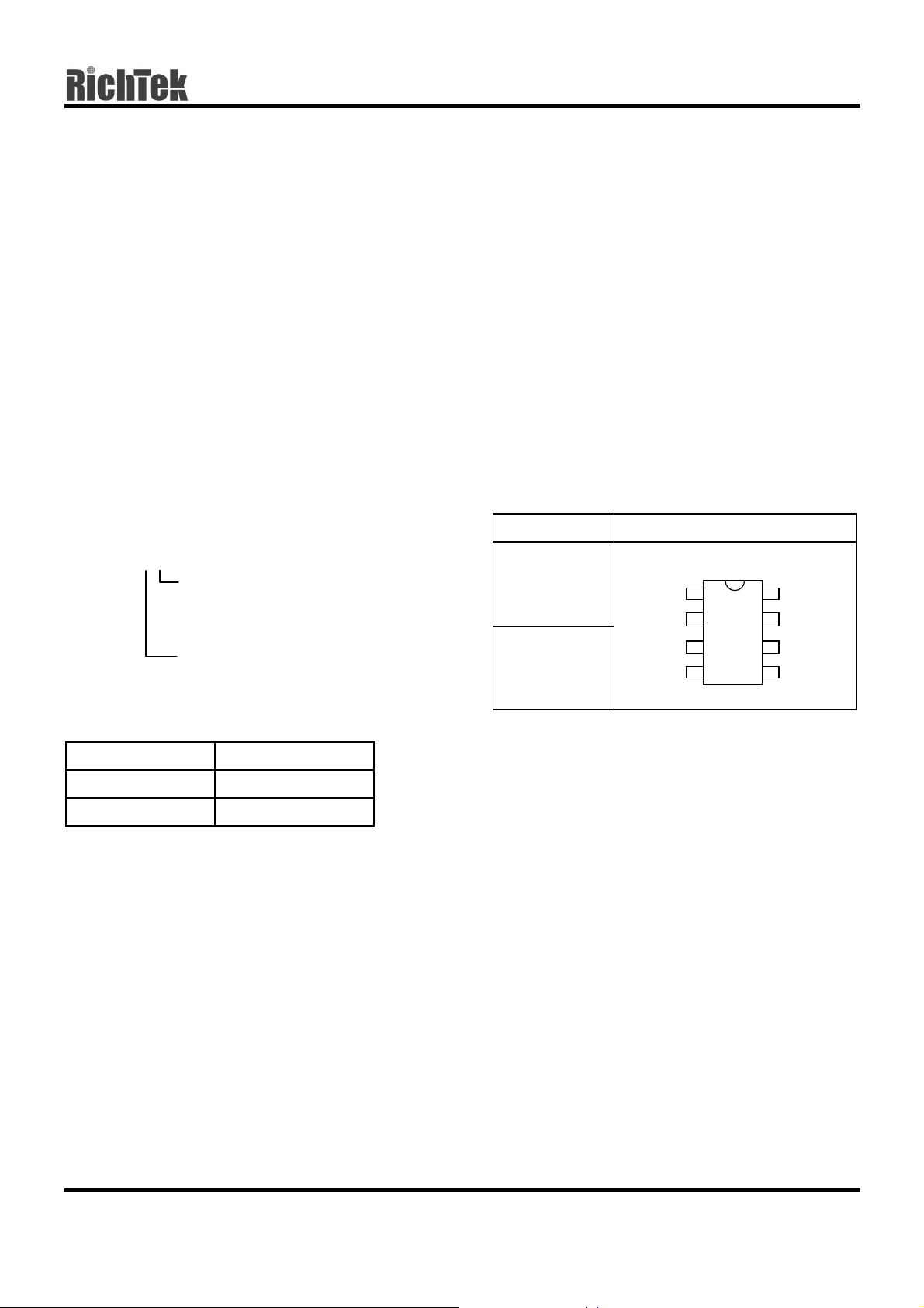
Pin Configurations
Part Number Pin Configurations
SC
SE
TC
GND
TOP VIEW
1
2
3
4
RT34063ACN
(Plastic DIP-8)
RT34063ACS
(Plastic SOP-8)
8
7
6
5
DRIVER
IPK
VCC
COMP
Marking Information
Part Number Marking
RT34063ACN RT34063ACN
RT34063ACS RT34063ACS
DS34063A-06 May 2001 www.richtek-ic.com.tw
1
RT34063A
g p
Absolute Maximum Ratings
Power Supply Voltage 30V
z
Feedback Input Voltage Range -0.3 ~ +30V
z
Switch Collector Voltage 30V
z
Switch Emitter Voltage 30V
z
Switch Collector to Emitter Voltage 30V
z
Driver Collector Voltage 30V
z
Driver Collector Current (see Note 1) 100mA
z
Switch Current 1.5A
z
Power Dissipation, PD @ T
z
DIP-8 1.25W
SOP-8 0.625W
• Package Thermal Resistance
DIP-8, θ
SOP-8, θ
Operating Junction Temperature Range -40 ~ +125°C
z
Storage Temperature Range -65 ~ +150°C
z
JA
JA
= 25°C
A
100°C/W
160°C/W
Note: 1. Maximum package power dissipation limits must be observed.
Electrical Characteristics
(VCC = 5V, TA = 25°C, unless otherwise specified)
Parameter Symbol Test Conditions Min Typ Max Units
Oscillator
Frequency
Charge Current
Discharge Current
I
CHG
I
DISCHG
Discharge to Charge Current Ratio Pin 7 to VCC
Current Limit Sense Voltage
V
LIMITICHG
Output Switch
Saturation Voltage, Darlington Connection
Saturation Voltage, Darlington Connection
DC Current Gain
Collector Off-state Current
Comparator
= 0V, CT = 1.0nF
V
PIN5
5.0V ≤ VCC ≤ 30V
5.0V ≤ VCC ≤ 30V
= I
DISCHG
= 1.0A, Pins1, 8 connected
I
SW
= 1.0A, R
I
SW
PIN8
VCC, Forced β ≅ 20
I
= 1.0A, VCE = 5.0V
SW
= 30V
V
CE
= 82Ω to
26 38 48 kHz
25 36 43
160 250 290
µA
µA
5.5 6.9 7.9 --
280 330 380 mV
-- 1.0 1.3 V
-- 0.45 0.7 V
50 75 -- --
-- 0.01 100
µA
Threshold Voltage
Threshold Voltage Line Regulation
Input Bias Current
I
BIAS
3.0V ≤ VCC ≤ 30V
VIN = 0V
1.225 1.25 1.275 V
-- 1.4 5.0 mV
-- -20 -400 nA
Total Device
VCC = 5.0V to 30V, CT = 1.0nF
Supply Current
www.richtek-ic.com.tw DS34063A-06 May 2001
I
CC
Pin7 = VCC, V
PIN5
= GND, Remainin
> VTH, Pin2
ins open
,
-- 3.0 4.5 mA
2
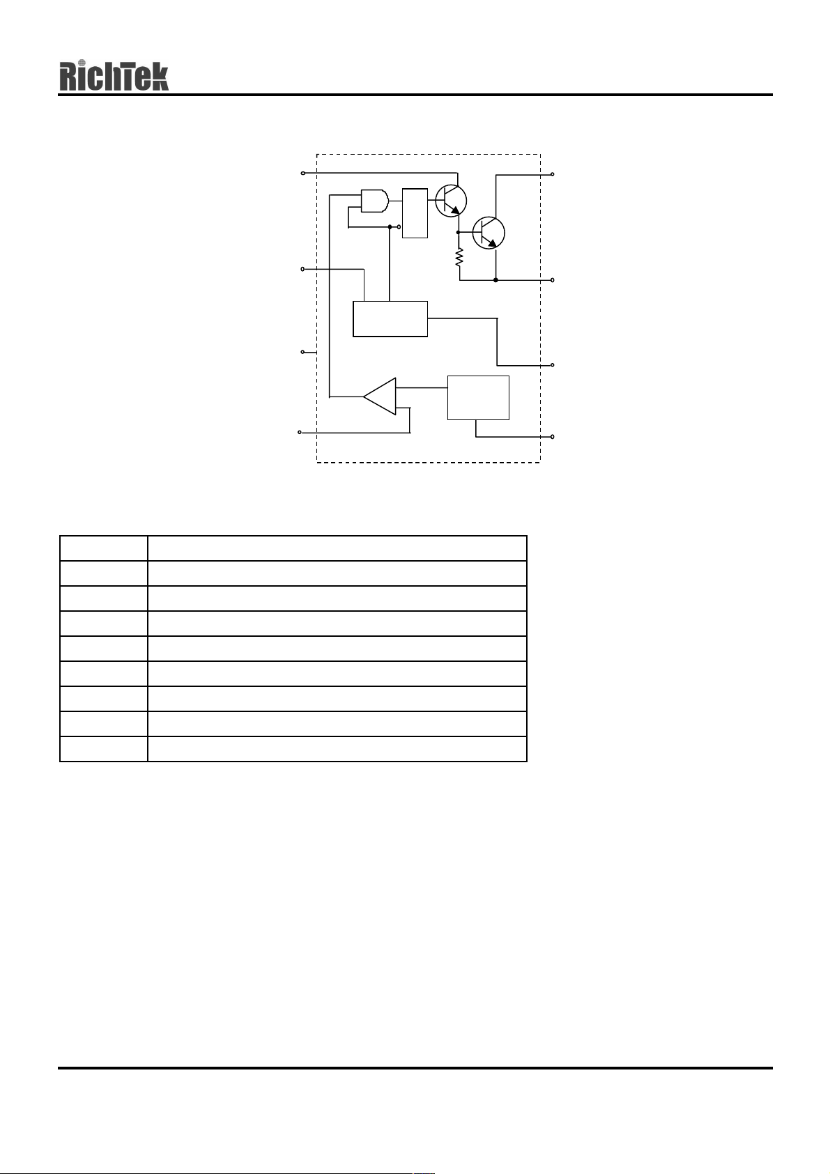
RT34063A
Function Block Diagram
Pin Description
Pin Name Pin Function
DRIVER
IPK
VCC
COMP
8
100
Reference
Regulator
Q2
1.25V
SQ
R
7
I
PK
Oscillator
6
Comparator
5
C
T
+
_
Q1
1
SC
2
SE
3
CT
4
GND
SC 1.5A Switch Collector
SE Darlington Switch Emitter
CT Oscillator Timing Capacitor
GND Power GND
COMP Feedback Comparator Inverting Input
VCC Power Supply Input
IPK
Highside Current Sense Input VCC-V
DRIVER Driver Collector
= 330mV
IPK
DS34063A-06 May 2001 www.richtek-ic.com.tw
3
RT34063A
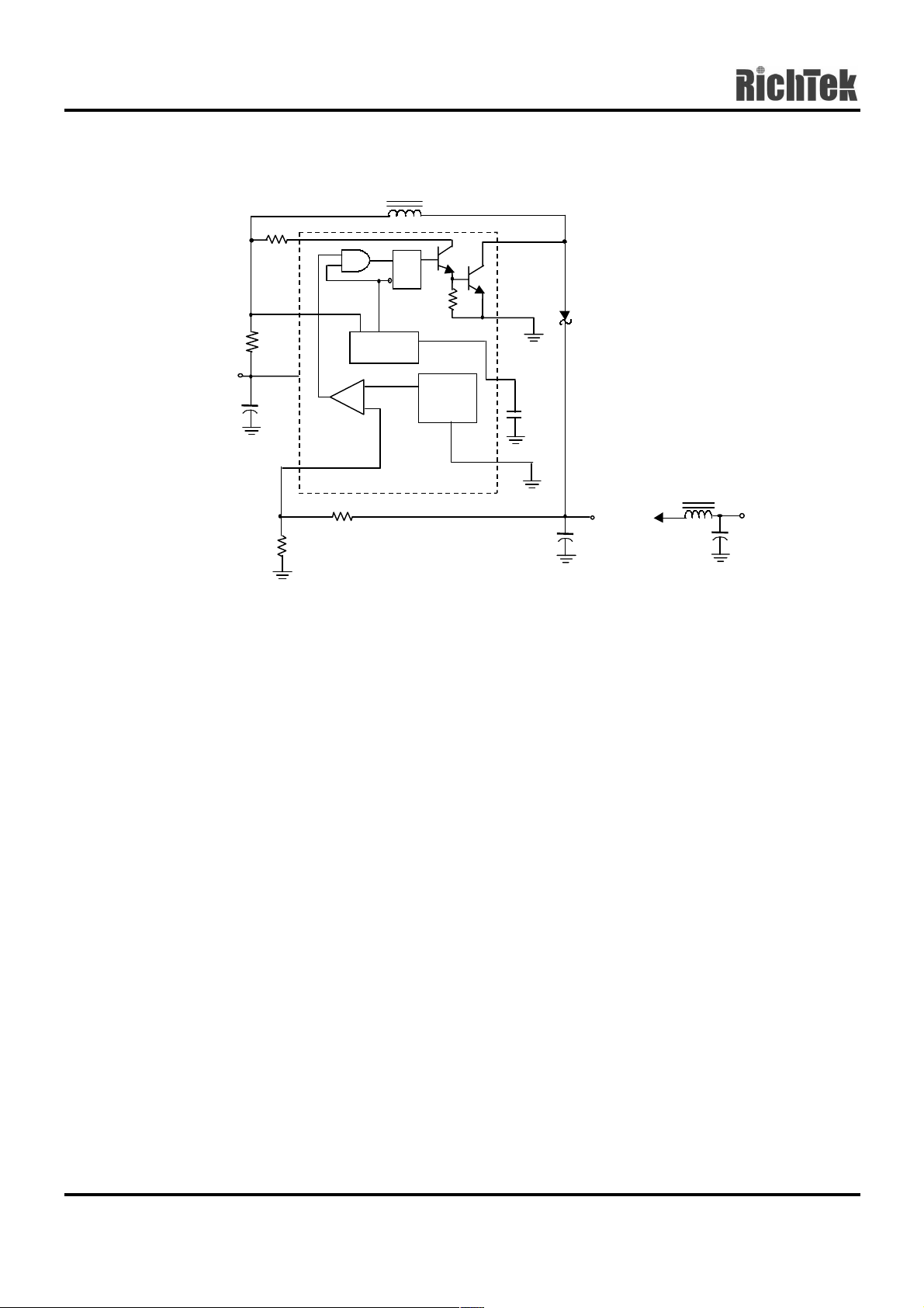
Typical Application Circuit
170µH
R
0.22
V
IN
12V
SC
180
+
100µF
8
7
6
5
2.2k
R1
L
SRQ
I
C
R2
47k
+
_
PK
OSC
Comp.
T
1.25V
Ref
Fig.1 Step-up Converter
1
2
C
T
3
1500 pF
4
330µF
1N5819
+
C
O
V
OU T
28V/17 5mA
Optional Filter
1.0µH
+
100µF
V
OUT
www.richtek-ic.com.tw DS34063A-06 May 2001
4
RT34063A
V
8
1
OU T
+
7
V
IN
6
5
2
3
4
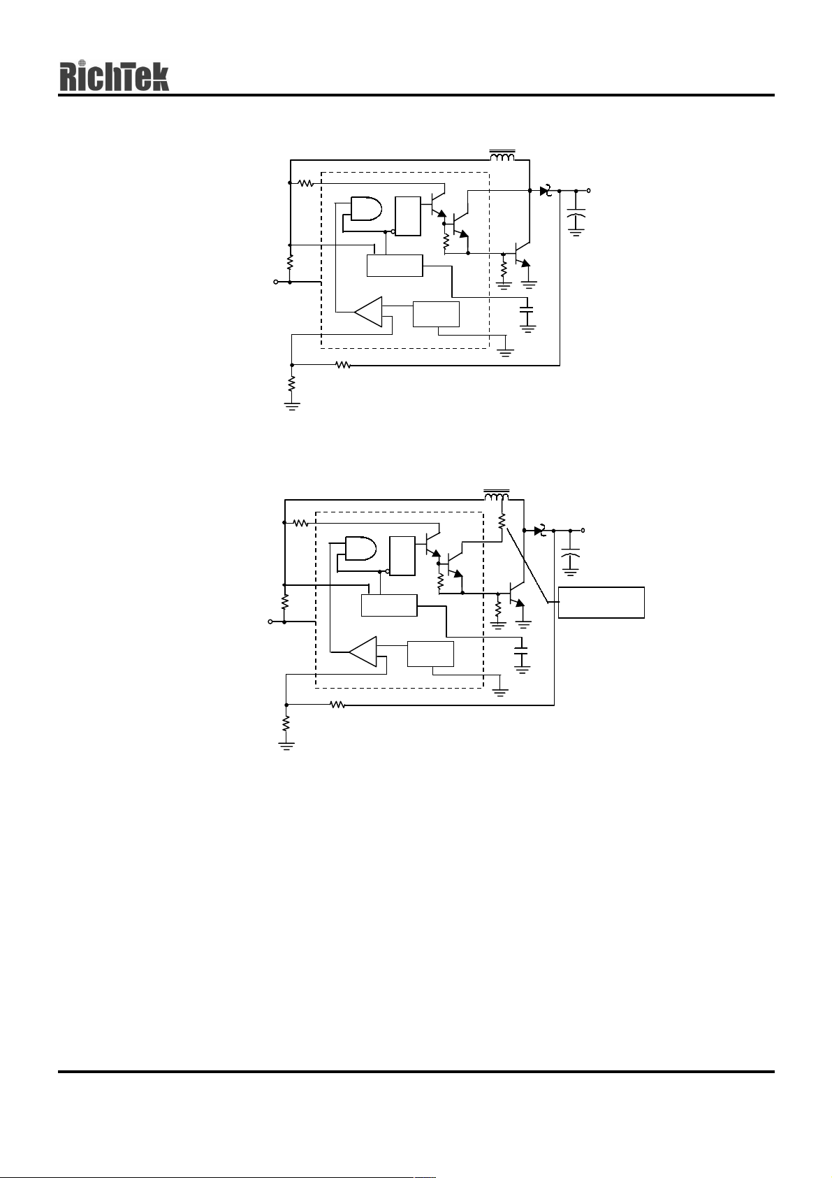
Fig.2a External NPN Switch
8
7
V
IN
6
R
1
2
3
V
OU T
+
R→0 for
Constant V
IN
5
4
Fig.2b External NPN Saturated Switch (See Note)
Fig.2 External Current Boost Connections for I
Peak Greater than 1.5A
C
Note: If the output switch is driven into hard saturation (non-Darlington configuration) at low switch currents
(≤ 300mA) and high driver currents (≥ 30mA), it may take up to 2.0µs to come out of saturation. This
condition will shorten the off time at frequencies ≥ 30KHz, and is magnified at high temperature. This
condition does not occur with a Darlington configuration, since the output switch cannot saturate. If a non-
Darlington configuration is used, the following output drive condition is recommended.
DS34063A-06 May 2001 www.richtek-ic.com.tw
5

RT34063A
R
SC
0. 33
V
IN
25V
+
100µF
8
7
6
5
R1
1. 2k
Q2
T
1. 25 V
Ref
R2
3. 6K
+
_
I
PK
SRQ
C
OSC
Comp.
Fig.3 Step-down Converter
Q1
1
1N58 19
2
3
C
470pF
4
470µF
T
C
O
L
220µH
+
Optional Filter
V
OU T
5.0V/500 mA
1. 0µH
+
100µF
V
OUT
www.richtek-ic.com.tw DS34063A-06 May 2001
6

RT34063A
8
1
7
V
IN
6
5
2
3
4
V
OU T
+
Fig.4a External NPN Switch
8
1
7
2
V
OU T
+
V
IN
6
3
5
4
Fig.4b External PNP Saturated Switch
Fig.4 External Current Boost Connections for IC Peak Greater than 1.5A
DS34063A-06 May 2001 www.richtek-ic.com.tw
7

RT34063A
R
SC
0.24
V
4.5V t o 6.0V
Q1
1
2
88µH
3
1500 pF
4
1000µF
L
1N58 19
Optional Filter
1.0µH
100µF
+
V
OUT
V
C
O
+
OU T
-12V/100mA
8
180
7
+
100µF
6
5
8.2k
R2
R1
953
IN
I
+
_
PK
SRQ
C
OSC
Comp.
Q2
T
1.25V
Ref
Fig.5 Voltage Inverting Converter
www.richtek-ic.com.tw DS34063A-06 May 2001
8

RT34063A
8
7
6
5
1
2
V
OUT
3
4
+
Fig.6a External NPN Switch
8
7
V
IN
6
5
1
V
OUT
2
3
4
+
Fig.6b External PNP Saturated Switch
Fig.6 External Current Boost Connections for Peak Greater than 1.5A
DS34063A-06 May 2001 www.richtek-ic.com.tw
9

RT34063A
(
)
Design Formula Table
Calculation Step-up Step-down Voltage-Inverting
+
ton/t
(ton + t
t
off
off
off
+
VV
(MIN) INFOUT
VVV
−+
SAT(MIN) IN
VV
−
)
1
f
+
tt
offon
on
t
+
1
off
t
on
t
off
t
FOUT
−−
OUTSAT(MIN) IN
VVV
1
f
+
tt
offon
+
1
VV
SATIN
−
VV
1
f
+
tt
offon
on
t
+
1
off
t
FOUT
t
on
C
T
Ipk
SWITCH
R
SC
(min) L
C
O
V
SAT
V
: Forward voltage drop of the output rectifier.
F
: Saturation voltage of the output switch.
()
×
I 2
0.3/Ipk
()
Ipk
−
(SWITCH)
OUT
9
ttt −+
offoffon
−
5
t104.0
on
t
on
(MAX) OUT
off
t
(SWITCH)
VV
SAT)MIN(IN
ton I
(pp) Vripple
+1
t
)MAX(on
()
×
I 2
0.3/Ipk
()
−
Ipk
V8
ttt −+
offoffon
−
5
t104.0
on
(MAX) OUT
(SWITCH)
VV
SAT)MIN(IN
)SWITCH(
)pp(ripple
t
)MAX(on
)tt(I +
offon)SWITCH(pk
()
The following power supply characteristics must be chosen:
V
V
I
OUT
IN
OUT
: Nominal input voltage.
: Desired output voltage
: Desired output current.
OUT
R
2
125.1V
+=
R
1
f : Minimum desired output switching frequency at the selected values of Vin and I
V
ripple(pp)
: Desired peak-to-peak output ripple voltage. In practice, the calculated capacitor value needs to be
increased due to its equivalent series resistance and board layout. The ripple voltage should be kept
to a low value since it directly affects the line and load regulation.
()
×
OUT(MAX)
0.3/Ipk
−
Ipk
9
O.
−
5
t
I 2
t
(SWITCH)
VV
SAT)MIN(IN
)SWITCH(
ton I
OUT
(pp) Vripple
ttt −+
offoffon
t104.0
on
on
+1
off
t
)MAX(on
www.richtek-ic.com.tw DS34063A-06 May 2001
10

RT34063A
Package Information
B
A
E
L
C
I
D
Symbol
A 9.068 9.627 0.357 0.379
B 6.198 6.604 0.244 0.260
C -- 4.318 -- 0.170
D 0.356 0.559 0.014 0.022
E 1.397 1.651 0.055 0.065
F
Dimensions In Millimeters Dimensions In Inches
Min Max Min Max
J
F 2.337 2.743 0.092 0.108
I 3.048 3.556 0.120 0.140
J 7.366 8.255 0.290 0.325
L 0.381 -- 0.015 --
8-Lead DIP Plastic Package
DS34063A-06 May 2001 www.richtek-ic.com.tw
11

RT34063A
H
A
M
B
J
F
C
D
Dimensions In Millimeters Dimensions In Inches
Symbol
Min Max Min Max
A 4.801 5.004 0.189 0.197
B 3.810 3.988 0.150 0.157
C 1.346 1.753 0.053 0.069
D 0.330 0.508 0.013 0.020
F 1.194 1.346 0.047 0.053
H 0.178 0.254 0.007 0.010
I 0.102 0.254 0.004 0.010
J 5.791 6.198 0.228 0.244
M 0.406 1.270 0.016 0.050
8–Lead SOP Plastic Package
I
www.richtek-ic.com.tw DS34063A-06 May 2001
12

RT34063A
DS34063A-06 May 2001 www.richtek-ic.com.tw
13

RT34063A
RICHTEK TECHNOLOGY CORP.
Headquarter
6F, No. 35, Hsintai Road, Chupei City
Hsinchu, Taiwan, R.O.C.
Tel: (8863)5510047 Fax: (8863)5537749
www.richtek-ic.com.tw DS34063A-06 May 2001
RICHTEK TECHNOLOGY CORP.
Taipei Office (Marketing)
8F-1, No. 137, Lane 235, Paochiao Road, Hsintien City
Taipei County, Taiwan, R.O.C.
Tel: (8862)89191466 Fax: (8862)89191465
Email: marketing@richtek-ic.com.tw
14
 Loading...