


Richtek RT8008-12PB, RT8008-12PJ5, RT8008-15PB, RT8008-15PJ5, RT8008-18PB Schematic [ru]
...
RT8008
1.5MHz, 600mA, High Efficiency PWM Step-Down DC/DC
Converter
General Description
The RT8008 is a high-efficiency pulse-width-modulated
(PWM) step-down DC/DC converter . Ca pable of delivering
600mA output current over a wide input voltage ra nge from
2.5V to 5.5V, the RT8008 is ideally suited for portable
electronic devices that are powered from 1-cell Li-ion
battery or from other power sources within the range such
a s cellular phones, PDAs and ha ndy-terminals.
Internal synchronous rectifier with low R
DS(ON)
dramatically
reduces conduction loss at PWM mode. No external
Schottky diode is required in practical application. The
RT8008 automatically turns off the synchronous rectifier
while the inductor current is low and enters discontinuous
PWM mode. This can increase efficiency at light load
condition.
The RT8008 enters Low-Dropout mode when normal PWM
cannot provide regulated output voltage by continuously
turning on the upper P-MOSFET . RT8008 enter shutdown
mode and consumes less tha n 0.1μA when EN pin is pulled
low.
The switching ripple is easily smoothed-out by small
package filtering elements due to a fixed operation
frequency of 1.5MHz. This along with small SOT-23-5 a nd
TSOT-23-5 pa ckage provides small PCB area a pplication.
Other features include soft start, lower internal reference
voltage with 2% accuracy, over temperature protection,
and over current protection.
Pin Configurations
(TOP VIEW)
FB/VOUT
5
EN
SOT-23-5/TSOT-23-5
VIN
4
23
GND LX
Marking Information
Features
zz
2.5V to 5.5V Input Range
z
zz
zz
z Adjustable Output From 0.6V to V
zz
zz
z 1.0V, 1.2V, 1.5V, 1.8V, 2.5V and 3.3V Fixed/
zz
IN
Adjustable Output Voltage
zz
z 600mA Output Current, 1A Peak Current
zz
zz
z 95% Efficiency
zz
zz
z No Schottky Diode Required
zz
zz
z 1.5MHz Fixed Frequency PWM Operation
zz
zz
z Small SOT-23-5 and TSOT-23-5 Package
zz
zz
z RoHS Compliant and 100% Lead (Pb)-Free
zz
Applications
z Cellular T elephones
z Personal Information Appliances
z Wireless and DSL Modems
z MP3 Players
z Portable Instruments
Ordering Information
RT8008(- )
Package Type
B : SOT-23-5
J5 : TSOT-23-5
Lead Plating System
P : Pb Free
G : Green (Halogen Free and Pb Free)
Output Voltage
Default : Adjustable
10 : 1.0V
12 : 1.2V
15 : 1.5V
18 : 1.8V
25 : 2.5V
33 : 3.3V
Note :
Richtek products are :
` RoHS compliant and compatible with the current require-
ments of IPC/JEDEC J-STD-020.
` Suitable for use in SnPb or Pb-free soldering processes.
For marking information, contact our sales re presentative
directly or through a Richtek distributor located in your
area.
DS8008-07 March 2011 www.richtek.com
1
RT8008
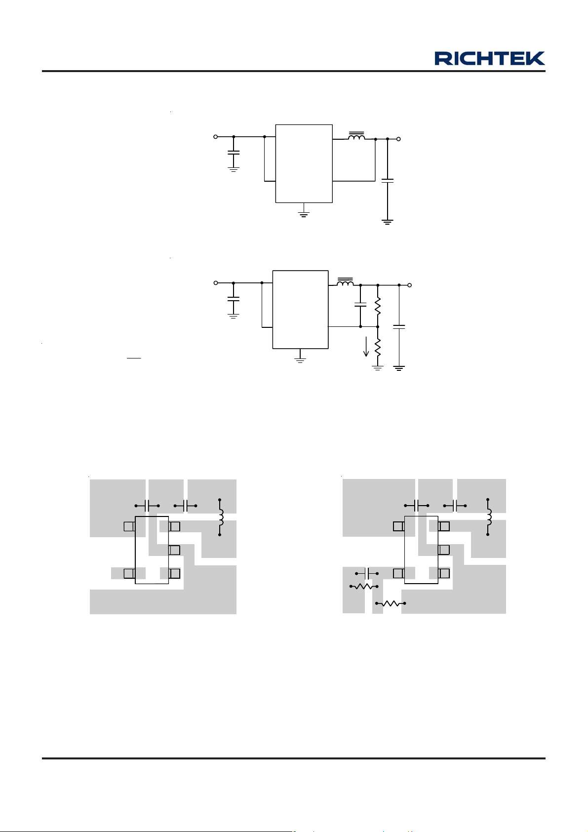
Typical Application Circuit
V
IN
2.2V to 5.5V
V
IN
2.2V to 5.5V
R1
⎛
REFOUT
⎜
⎝
⎞
+=
1 x VV
⎟
R2
⎠
with R2 = 300kΩ to 60kΩ so the IR2 = 2μA to 10μA,
C
IN
4.7µF
Figure 1. Fixed Voltage Regulator
C
IN
4.7µF
4
1
4
1
VIN
EN
VIN
RT8008
EN
RT8008
VOUT
GND
2
GND
2
LX
FB
LX
3
5
2.2µH
3
5
2.2µH
L
I
L
R2
C1
R1
R2
V
C
OUT
10µF
OUT
V
C
OUT
10µF
OUT
and (R1 x C1) should be in the range between 3x10⁻⁶ and 6x10⁻⁶ for component selection.
Figure 2. Adjustable Voltage Regulator
Layout Guide
V
IN
VOUT
VIN
4
5
C
IN
GND
GND
3
2
1
C
OUT
LX
GND
EN
V
OUT
L
V
OUT
R1
V
C1
IN
VIN
FB
R2
C
IN
4
5
Figure 3
Layout note:
1. The distance that C
2. C
should be placed near RT8008.
OUT
connects to VIN is as close as possible (Under 2mm).
IN
GND
3
2
1
C
GND
OUT
LX
GND
EN
V
OUT
L
DS8008-07 March 2011www.richtek.com
2
Functional Pin Description
Pin Number Pin Name Pin Function
1 EN Chip Enable (Active High, do not leave EN pin floating, and VEN < VIN + 0.6V).
2 GND Ground.
3 LX Pin for Switching.
4 VIN Power Input.
5 FB/VOUT Feedback Input Pin.
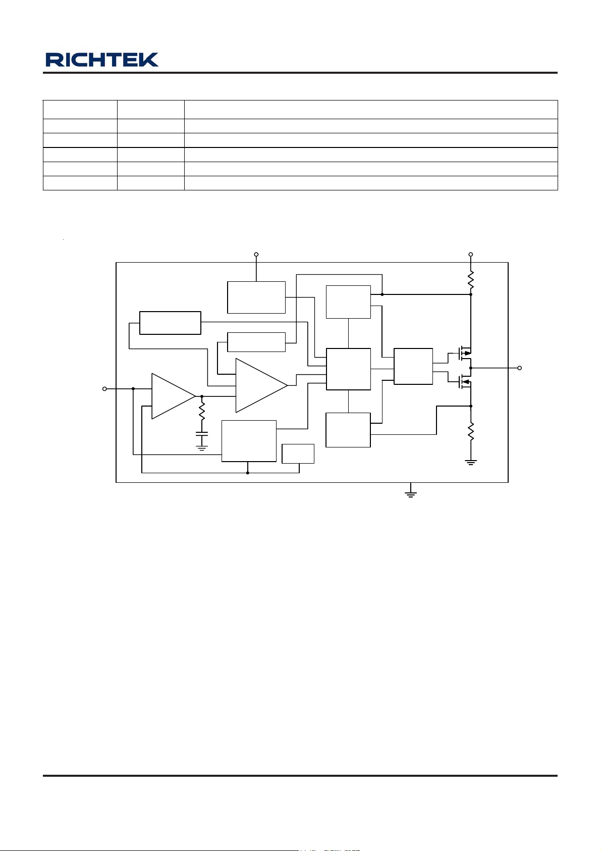
Function Block Diagram
RT8008
FB/VOUT
Slope
Compensation
Error
Amplifier
RC
COMP
EN
OSC &
Shutdown
Control
Current
Sense
PWM
Comparator
UVLO &
Power Good
Detector
V
REF
Current
Limit
Detector
Control
Logic
Zero
Detector
Driver
GND
VIN
RS1
LX
RS2
DS8008-07 March 2011 www.richtek.com
3
RT8008
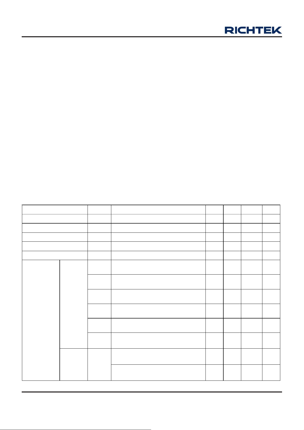
Absolute Maximum Ratings (Note 1)
Supply Input Voltage ------------------------------------------------------------------------------------------------------ 6.5V
Enable, FB Voltage ------------------------------------------------------------------------------------------------------- V
Power Dissipation, P
@ TA = 25°C
D
SOT-23-5, TSOT-23-5 ----------------------------------------------------------------------------------------------------- 0.4W
Package Thermal Resistance (Note 2)
SOT-23-5, TSOT-23-5, θJA----------------------------------------------------------------------------------------------- 250°C/W
SOT-23-5, TSOT-23-5, θJC----------------------------------------------------------------------------------------------- 130°C/W
Junction Temperature Range-------------------------------------------------------------------------------------------- 150°C
Lead Temperature (Soldering, 10 sec.) ------------------------------------------------------------------------------- 260°C
Storage Temperature Range -------------------------------------------------------------------------------------------- −65°C to 150°C
ESD Susceptibility (Note 3)
HBM (Human Body Mode) ---------------------------------------------------------------------------------------------- 2kV
MM (Machine Mode) ------------------------------------------------------------------------------------------------------ 200V
Recommended Operating Conditions (Note 4)
Supply Input Voltage ------------------------------------------------------------------------------------------------------ 2.5V to 5.5V
Junction Temperature Range-------------------------------------------------------------------------------------------- −40°C to 125°C
Ambient Temperature Range -------------------------------------------------------------------------------------------- −40°C to 85°C
+ 0.6V
IN
Electrical Characteristics
(V
= 3.6V, V
IN
Input Voltage Range
Quiescent Current
Shutdown Current
Refere nce Voltage
Adjustable Output Range
Output V olt age
Accuracy
4
OUT
= 2.5V, V
= 0.6V, L = 2.2μH, C
REF
Parameter Symbol Test Conditions Min Typ Max Unit
V
IN
I
I
Q
I
SHD N
V
REF
V
OUT
ΔV
OU T
ΔV
OU T
ΔV
OU T
Fix
ΔV
OU T
ΔV
OU T
ΔV
OU T
Adj ustable
ΔV
OU T
= 4.7μF, C
IN
OUT
= 10μF, T
= 25°C, I
A
= 600mA unless otherwise specified)
MAX
2.5 -- 5.5 V
= 0mA, VFB = V
OUT
REF
+ 5%
EN = GND -- 0.1 1
-- 50 100
μA
μA
For adjustable output voltage 0.588 0.6 0.612 V
V
= 2.2 to 5.5V, V
IN
0A < I
V
IN
0A < I
V
IN
0A < I
V
IN
0A < I
V
IN
0A < I
V
IN
0A < I
VIN = V
0A < I
V
IN
0A < I
< 600mA
OUT
= 2.2 to 5.5V, V
< 600mA
OUT
= 2.2 to 5.5V, V
< 600mA
OUT
= 2.2 to 5.5V, V
< 600mA
OUT
= 2.8 to 5.5V, V
< 600mA
OUT
= 3.5 to 5.5V, V
< 600mA
OUT
OUT
< 600mA
OUT
= V
OUT
< 600mA
OUT
= 1.0V
OU T
= 1.2V
OU T
= 1.5V
OU T
= 1.8V
OU T
= 2.5V
OU T
= 3.3V
OU T
+ 0.2V to 5.5V, VIN ≧ 3.5V
+ 0.4V to 5.5V, VIN ≧ 2.2V
V
REF
−3 -- 3 %
−3
−3
−3
−3
−3
−3 -- 3 %
−3
--
V
− 0.2
IN
-- 3 %
-- 3 %
-- 3 %
-- 3 %
-- 3 %
-- 3 %
V
To be continued
DS8008-07 March 2011www.richtek.com
RT8008
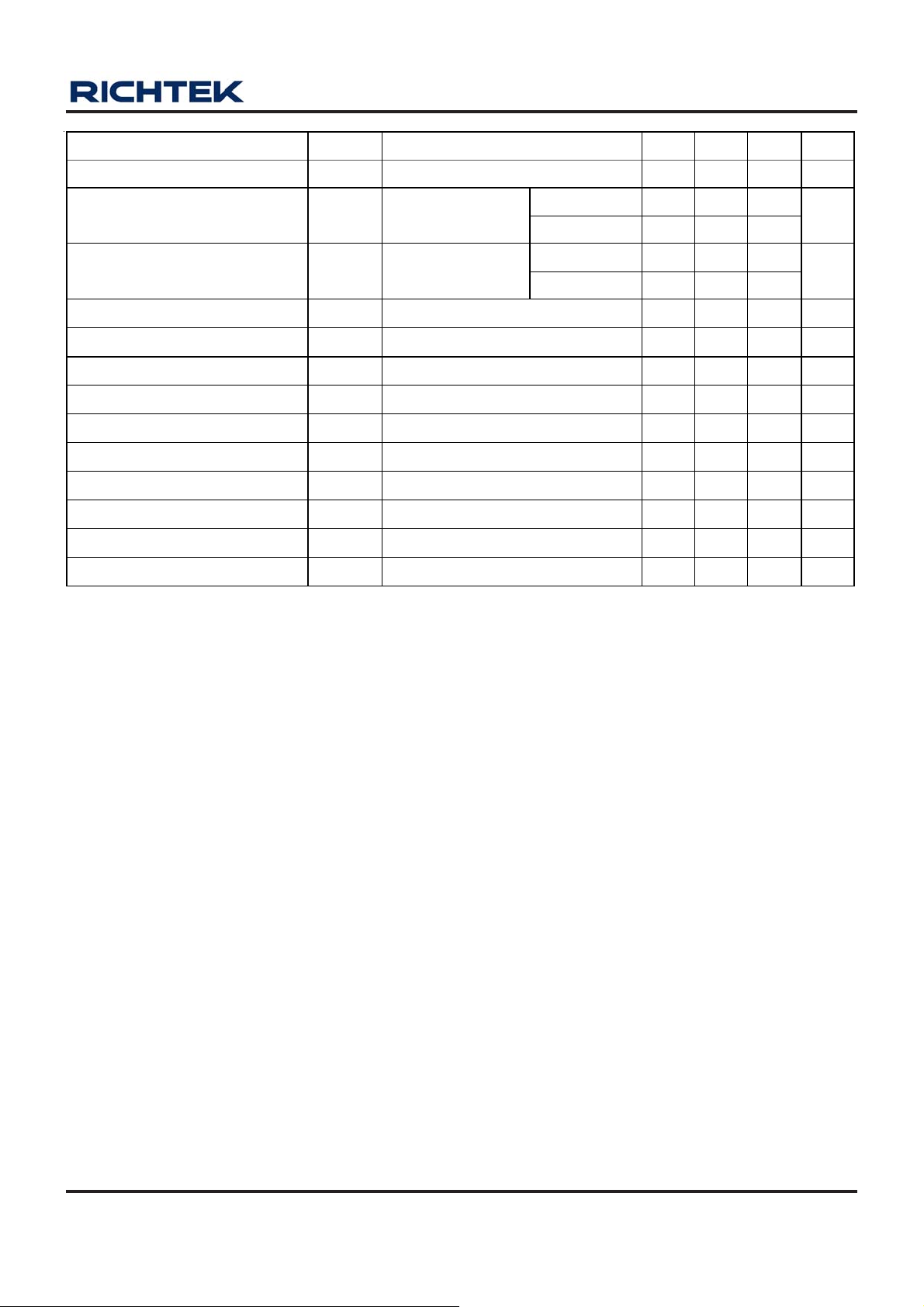
Parameter Symbol Test Conditions Min Typ Max Unit
FB Input Current
PMOSFET RON P
NMOSFET RON N
P-Channel Current Limit
EN High-Level Input Voltage
EN Low-Level Input Voltage
I
V
FB
RDS(ON)
RDS(ON)
I
V
P(LM)
V
VIN = 2.5V to 5.5V
ENH
V
VIN = 2.5V to 5.5V
ENL
= V
FB
I
= 200mA
OUT
I
= 200mA
OUT
= 2.5V to 5.5 V
IN
IN
V
= 3.6V
IN
V
= 2.5V
IN
V
= 3.6V
IN
V
= 2.5V
IN
−50 -- 50 nA
-- 0.3 --
Ω
-- 0.4 --
-- 0.25 --
Ω
-- 0.35 --
1 -- 1.8 A
1.5 -- -- V
-- -- 0.4 V
Under Voltage Lockout Threshold -- 1.8 -- V
Hysteresis -- 0.1 -- V
Oscillator Frequency
Thermal Shutdown Temperature
V
f
OSC
T
SD
= 3.6V, I
IN
OUT
= 100mA
-- 160 -- °C
1.2 1.5 1.8 MHz
Min. On Time -- 50 -- ns
Max. Duty Cycle 100 -- -- %
LX Leakage Current V
Note 1. Stresses listed as the above “Absolute Maximum Ratings” may cause permanent damage to the device. These are for
stress ratings. Functional operation of the device at these or any other conditions beyond those indicated in the
operational sections of the specifications is not implied. Exposure to absolute maximum rating conditions for extended
periods may remain possibility to affect device reliability.
Note 2. θ
Note 3. Devices are ESD sensitive. Handling precaution recommended.
Note 4. The device is not guaranteed to function outside its operating conditions.
is measured in the natural convection at TA = 25°C on a low effective single layer thermal conductivity test board of
JA
JEDEC 51-3 thermal measurement standard. Pin 2 of SOT-23-5/TSOT-23-5 packages is the case position for θ
measurement.
= 3.6V, V
IN
= 0V or V
LX
= 3.6V −1 -- 1 μA
LX
JC
DS8008-07 March 2011 www.richtek.com
5
 Loading...