

RT8203
High-Efficiency, Quad Output, Main PowerControllers for Notebook Computers
General Description
The RT8203 dual step-down, Switch Mode Power Supply
(SMPS) controllers generate logic-supply voltages in
battery-powered systems. The RT8203 include two pulsewidth modulation (PWM) controllers, adjustable from 2V
to 5.5V or fixed at 5V a nd 3.3V . These devices feature two
linear regulators providing 5V and 3.3V always-on outputs.
Each linear regulator provides up to 100mA output current
with automatic linear regulator bootstrapping to the main
SMPS outputs. The RT8203 include on-board power-up
sequencing, a power good (PGOOD) output, internal softstart, and soft-shutdown output discharge that prevents
negative voltages on shutdown. Richtek's proprietary Mach-
PWMTM “instant-on” response, constant on-time PWM
control scheme operates without sense resistors and
provides 100ns response to load transients while
maintaining a relatively constant switching frequency . The
unique ultrasonic mode maintain s the switching frequency
above 25kHz, which eliminates noise in audio a pplications.
Other features include diode-emulation, which maximizes
efficiency in light-load applications, and fixed-frequency
PWM mode, which reduces RF interference in sensitive
applications. The RT8203 provides a pin-selectable
switching frequency, allowing either 200kHz/300kHz or
400kHz/500kHz operation of the 5V/3.3V SMPSs,
respectively . The RT8203 is available in SSOP-28 package.
Ordering Information
RT8203
Package Type
A : SSOP-28
Lead Plating System
P : Pb Free
G : Green (Halogen Free and Pb Free)
Note :
Richtek products are :
` RoHS compliant and compatible with the current require-
ments of IPC/JEDEC J-STD-020.
` Suitable for use in SnPb or Pb-free soldering processes.
Features
zz
z No Current Sense Resistor Needed
zz
zz
z 1.5% Output V oltage Accura cy
zz
zz
z 3.3V and 5V 100mA Bootstra pped Linear Regulators
zz
zz
z Internal Soft-Start and Soft-Shutdown Output
zz
Discharge
zz
z Mach-PWM with 100ns Load Step Response
zz
zz
z 3.3V and 5V Fixed or Adjustable Outputs
zz
zz
z 7V to 24V Input Voltage Range
zz
zz
z Ultrasonic Mode Operation 25kHz (min.)
zz
zz
z Power Good (PGOOD) Signal
zz
zz
z Over Voltage Protection
zz
zz
z Under Voltage Protection
zz
zz
z Over Temperature Protection
zz
zz
z RoHS Compliant and 100% Lead (Pb)-Free
zz
Applications
z Notebook and Subnotebook Computers
z PDAs and Mobile Communication Devices
z 3- and 4-Cell Li+ Battery-Powered Devices
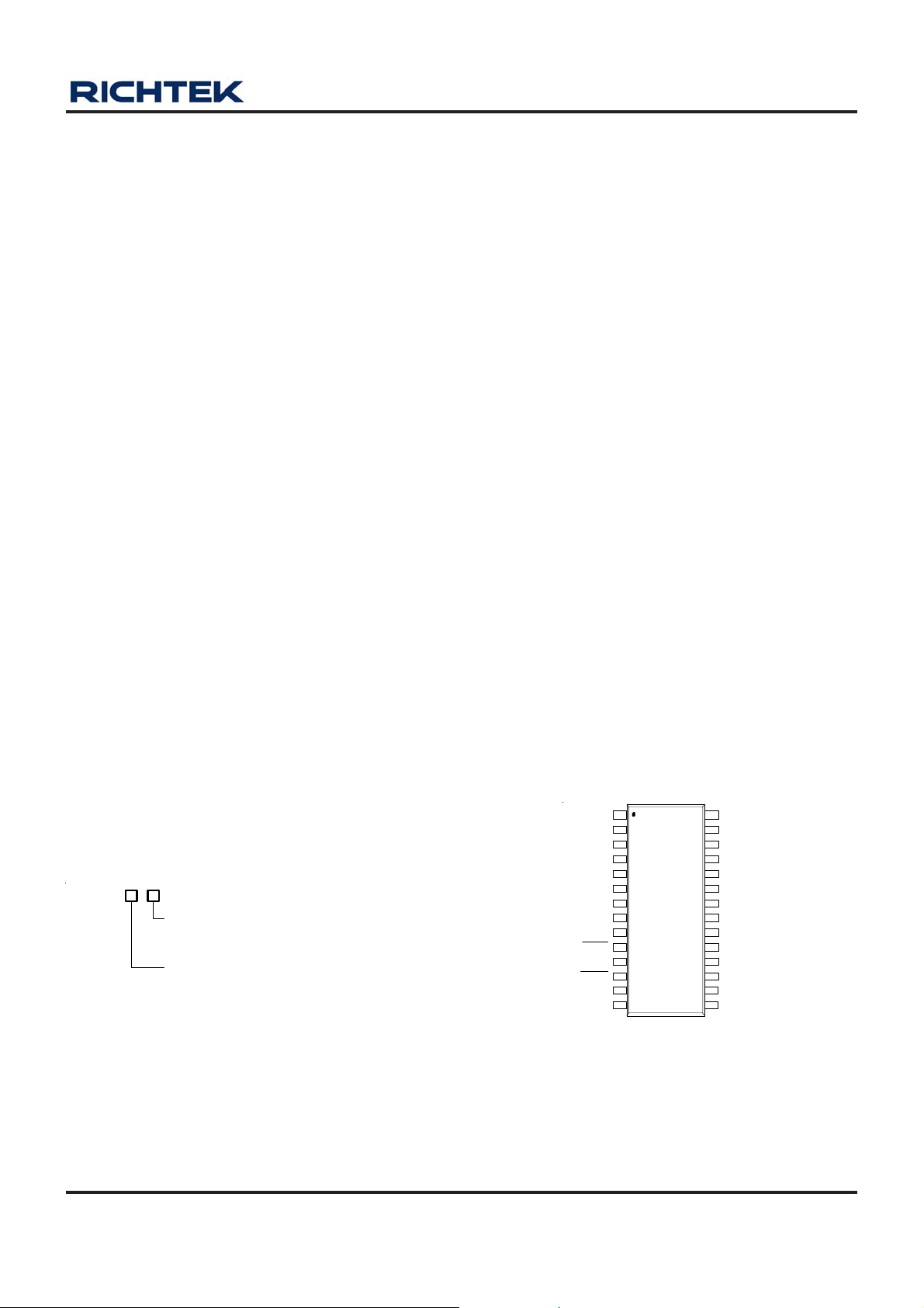
Pin Configurations
NC
PGOOD
ON3
ON5
ILIM3
EN
FB3
VREF
FB5
PRO
ILIM5
SKIP
TON
BOOT5
Supply
(TOP VIEW)
28
2
3
4
5
6
7
8
9
10
11
12
13
14
27
26
25
24
23
22
21
20
19
18
17
16
SSOP-28
15
SSOP-28
BOOT3
PHASE3
UGATE3
LDO3
LGATE3
GND
VOUT3
VOUT5
VIN
LGATE5
LDO5
VCC
UGATE5
PHASE5
DS8203-05 April 2011 www.richtek.com
1
RT8203
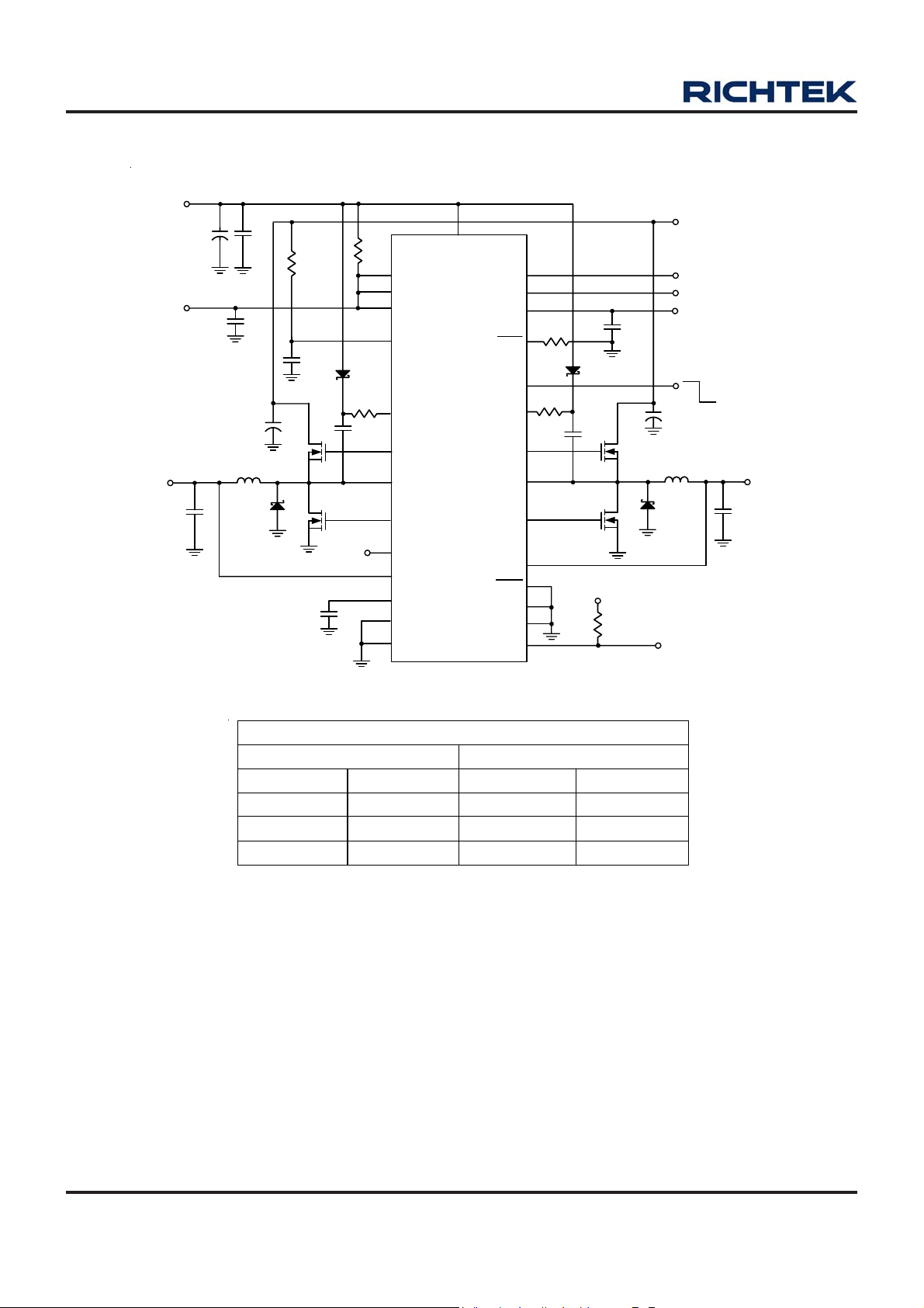
Typical Application Circuit
5V
ALWAYS ON
V
CC
V
OUT5
5V
C10
C1
4.7µF
+
C2
1µF
C3
1µF
C6
10µF
L1
AO4702
D3
R1
3.9
C5
0.1µF
Q1
C12
0.22µF
D1
BSC119N03
TABLE
BAT254
R3
2.2
C8
0.1µF
SEE
R2
47
17
5
11
20
14
16
15
19
13
21
8
9
23
VCC
ILIM3
ILIM5
VIN
BOOT5
UGATE5
PHASE5
LGATE5
TON
VOUT5
VREF
FB5
GND
18
LDO5
RT8203
V
IN
7V to 24V
3
ON3
4
ON5
25
LDO3 3.3V ALWAYS ON
PRO
BOOT3
UGATE3
PHASE3
LGATE3
VOUT3
SKIP
FB3
PGOOD
EN
NC
R6
1M
10
6
R4
2.2
28
26
27
24
BSC119N03
22
12
7
1
2
D2
BAT254
C9
0.1µF
V
CC
R5
100k
C4
4.7µF
Q2
AO4702
Q4Q3
V
REF
V
CC
ON
C7
10µF
L2
D4
Power-Good
INDICATOR
OFF
C11
V
OUT3
3.3V
Frequen cy-depe ndent Components
VOUT5 VOUT3
TON = VCC TON = GND TON = VCC TON = GND
f = 200kHz f = 400kHz f = 300kHz f = 500kHz
L1 = 7.6μH L1 = 5.6μH L2 = 4.7μH L2 = 3μH
C10 = 330μF C10 = 150μF C11 = 470μF C11 = 220μF
Figure 1. Fixed V oltage Regulator
DS8203-05 April 2011www.richtek.com
2
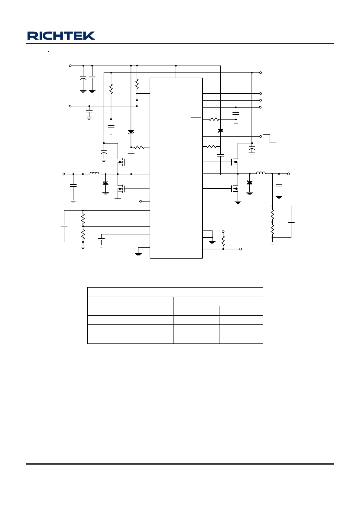
5V
ALWAYS ON
4.7µF
V
CC
V
OUT5
5V
C10
C13
0.1µF
C1
+
R7
15k
R8
10k
C2
1µF
C3
1µF
C6
10µF
L1
AO4702
D3
C12
0.22µF
R1
3.9
C5
0.1µF
Q1
BSC119N03
BAT254
D1
SEE
TABLE
R2
47
R3
2.2
C8
0.1µF
17
5
11
20
14
16
15
19
13
21
9
8
23
VCC
ILIM3
ILIM5
VIN
BOOT5
UGATE5
PHASE5
LGATE5
TON
VOUT5
FB5
VREF
GND
18
LDO5
RT8203
V
IN
7V to 24V
3
ON3
4
ON5
25
LDO3 3.3V ALWAYS ON
PRO
BOOT3
UGATE3
PHASE3
LGATE3
VOUT3
FB3
SKIP
PGOOD
EN
NC
R6
1M
10
6
R4
2.2
28
26
27
24
BSC119N03
22
7
12
1
2
D2
BAT254
C9
0.1µF
V
CC
100k
R5
C4
4.7µF
Q2
AO4702
Q4Q3
Power-Good
INDICATOR
C7
10µF
D4
L2
V
V
ON
REF
CC
OFF
R9
6.5k
R10
10k
RT8203
V
OUT3
3.3V
C11
C14
0.1µF
Frequen cy-depe ndent Components
VOUT5 VOUT3
TON = VCC TON = GND TON = VCC TON = GND
f = 200kHz f = 400kHz f = 300kHz f = 500kHz
L1 = 7.6μH L1 = 5.6μH L2 = 4.7μH L2 = 3μH
C10 = 330μF C10 = 150μF C11 = 470μF C11 = 220μF
Figure 2. Adjustable V oltage Regulator
DS8203-05 April 2011 www.richtek.com
3
RT8203
Functional Pin Description
Pin No. Pin Name Pin Function
1 NC Connect to GND.
2 PGOOD
3 ON3
4 ON5
5 ILIM3
6 EN
7 FB3
8 VREF
9 FB5
10
11 ILIM5
PRO
Po wer Goo d O p en D rain Outpu t. PGO OD is pul le d low if either outp ut i s disa ble or is
more than 8.75% bel ow its normal val ue.
VOUT 3 Enabl e In put. T he 3.3V SMP S i s ena ble if ON 3 is greater than the on leve l
and disa bl e i f ON3 is less t han the off l evel . If ON 3 i s co nnec ted to V
SMPS starts after the 5V SMPS reached regul ation(delay start). Force ON3 below the
clear fault level to reset the fault latched.
VOUT5 Enable Input. The 5V SMPS is enable if ON5 is greater than the on level and
disab le i f ON 5 is le ss than the off level . If ON 5 is connec ted t o VRE F, the 5 V SMP S
starts after the 3.3V SMPS reached regulation(delay start). Force ON5 below the clear
fault level to reset the fault latched.
VOUT3 Current Limit Adjustment. The GND-PHASE3 current limit threshold defaults
to 100mV if ILIM3 is tied to VCC. In adjustable mode, the current limit threshold is 1/10
the voltage seen at ILIM3 over 0.5V to 3V range. The logic threshold for switch over to
100mV default value is approxi mately VCC − 1V.
Enable Control Input. The device enters its 15μA supply current shutdown mode if EN
is less than the EN input falling edge trip level and does not restart until EN is greater
than the E N input risin g edg e tr ip lev el. Co nnect E N to VI N for auto mat icall y star tu p.
EN can be connected to VIN through a resistive voltage divider to implement a
programmable undervoltage lockout.
VOUT3 Feedback Input. Connect FB3 to GND for fixed 3.3V operation. Connect FB3
to a resistive voltage divider from VOUT3 to GND to adjust the output from 2V to 5.5V.
2V Reference Output. Bypass to GND with a 0.22μF
up to 10 0μA f or ex terna l l oad s. Loa din g V REF degr a des FBx and V O UTx accu ra cy
according to the VREF load regulation error.
VOUT5 Feedback Input. Connect FB5 to GND for fixed 5V operation. Connect FB5 to
a resistive voltage divider from VOUT5 to GND to adjust the output from 2V to 5.5V.
Over Vo lta ge and Under Voltage Fault P rotecti on En able/Disa ble. Conn ect PRO to
VCC to disabl e Over Voltage and Under Voltage protection. Connect PRO to GND to
enable Ov er Voltage and Under Voltage protection.
VOUT5 Current Limit Adjustment. The GND − PHASE5 cu rrent limit threshold defaults
to 100mV if ILIM5 is tied to VCC. In adjustable mode, the current limit threshold is 1/10
the voltage seen at ILIM5 over 0.5V to 3V range. The logic threshold for switch over to
100mV default value is approxi mately VCC − 1V.
REF
capacitor. VRE F can source
(MIN)
, the 3.3V
12
13 TON
14 BOOT5
4
SKIP
Operation Mode Input Control. Connect SKIP to GND for diode-emulation mode
(DEM ) or to VCC fo r CCM m ode(f ixed frequency). Conn ect to VREF or flo ating for
ultrason ic mode.
Fr eque ncy S elec t Inp ut. C onne ct to V CC f or 200 k Hz/300k Hz ope ratio n an d to G ND
for 400kHz /500kHz operation (VOUT5/VOUT3 switching frequency respectively).
Bo ost Capac i tor Conn ec tio n for 5V S MP S. Co nnect an e xt ernal c eram ic c apac itor to
PHAS E5 and an exte rnal diode t o LDO5.
To be continued
DS8203-05 April 2011www.richtek.com

Pin No. Pin Name Pin Function
15 PHASE5
16 UGATE5
17 VCC
18 LDO5
19 LGATE5
20 VIN
21 VOUT5
22 VOUT3
23 GND Anal og and Pow er Ground.
24 LGATE3
25 LDO3
26 UGATE3
27 PHASE3
28 BOOT3
Inductor Connection for 5V SMPS. PHASE5 is the internal lower supply rail for the
UGATE5 high side gate driv er , and the current sense input for the 5V SMPS.
High Side N-MOSFET Floating Gate-Driver Output for VOUT5. Swings between
PH ASE5 a nd BOOT 5.
Analog Supply Voltage Input for the inter nal analog integrated circuit. Bypass to GND
with a 1μF cera mic capaci tor.
5V Linear Regulator Output. LDO5 is the gate driver supply for the external
MOSFETs. LDO5 can provide a total of 100mA, including the MOSFET gate-driver
requirements and external loads. If VOUT5 is greater than the LDO5 switchover
threshold, the LDO5 regulator shuts down and LDO5 pin connects to VOUT5 through
a 1. 4Ω switch. Bypass a 4.7μF ceramic capacitor to GND.
Low side N-MOSFET Gate-Drive Output for VOUT5. Swings between GND and
LDO5.
Power-Supply Input. VIN powers the LDO5/LDO3 linear regulators and is also used
for PWM contr ol circuits. Connect VI N to the batter y input or the AC adapte r output .
VOUT5 Sense Input . Connec t to the 5V outp ut. VO UT5 is an i nput to the PWM co nt ro l
circuit. It also serves as the 5V feedback input in fixed-voltage mode. If VOUT5 is
greater than the LDO5 switchover threshold, the LDO5 shuts down and LDO5
co nnect s to VOUT 5 through 1.4Ω switch .
VOUT3 Sense Input. Connect to the 3.3V output. VOUT3 is an input to the PWM
control circuit. It also serves as the 3.3V feedback input in fixed voltage mode. If
VOUT3 is greater than the LDO3 switchover threshold, the LDO3 shuts down and
LDO 3 connects to VOUT3 throug h 1.5Ω swi t ch.
Low side N-MOSFET Gate-Drive Output for VOUT3. Swings between GND and
LDO5.
3.3V Linear Regulator Output . LDO 3 can provide a total of 100mA to external loads. If
VOUT3 is greater than the LDO3 switchover threshold, the LDO3 regulator shuts
down and LDO3 pin connects to VOUT3 through a 1.5Ω switch. Bypass a 4.7μF
ceramic capacitor to GND.
High Side N-MOSFET Floating Gate-Driver Output for VOUT3. Swings between
PH ASE3 a nd BOOT 3.
Inductor Connection f or 3.3V SMPS. PHASE3 is the internal lower supply rail for the
UGATE3 high side gate driv er, and th e current sense inpu t fo r the 3.3V SMPS.
Boost Capacitor Con nec tion f or 3.3V SMPS. Connect an ext er nal ceramic capacitor to
PHASE3 and an external diode to LDO5.
RT8203
DS8203-05 April 2011 www.richtek.com
5
RT8203
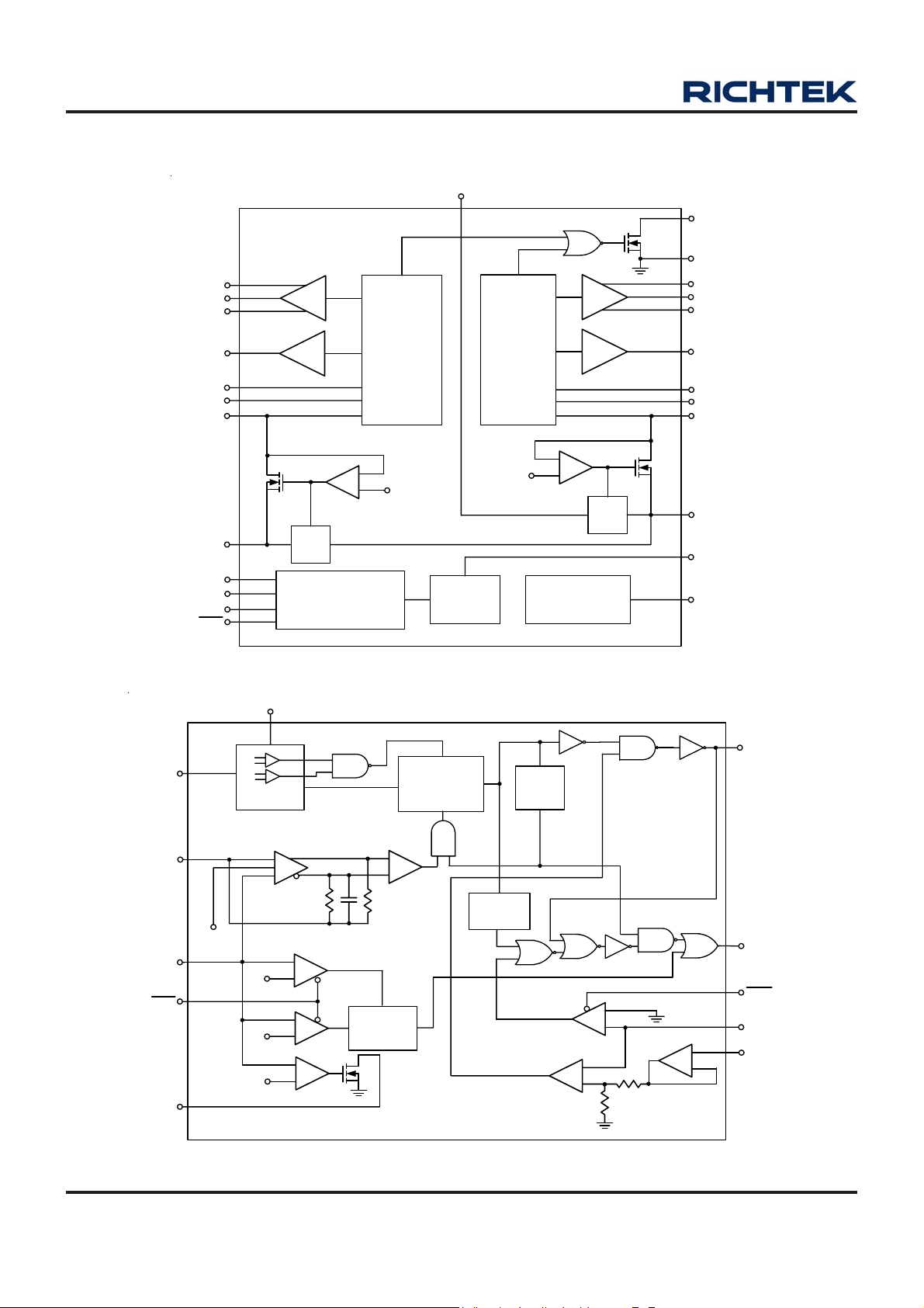
Function Block Diagram
BOOT3
UGATE3
PHASE3
LGATE3
ILIM3
FB3
VOUT3
Driver
Driver
VIN
U3 U5
VOUT3
L3 L5
PWM
Controller
VOUT5
PWM
Controller
Driver
Driver
PGOOD
GND
BOOT5
UGATE5
PHASE5
LGATE5
ILIM5
FB5
VOUT5
VOUTx
VREF
FBx
PRO
PGOOD
LDO3
ON3
ON5
EN
PRO
SS
(internal)
VIN
On-time
Compute
1.1xV
REF
0.7xV
REF
0.9xV
REF
EN3
LDO
(3V)
Power Sequence
+
GM
-
+
-
+
+
Logic
OV
UV
+
-
S2
2.93V
LDO5
+
Comp
S1
Latch
Thermal
Shutdown
1-SHOT
R
Ton
TRIG
Q
PWM Controller
Ton
QN
Detector
4.65V
25Khz
TRIG
QN
Min. Toff
1-SHOT
Detector
Current
Limit
+
-
2V
Reference
Zero
+
EN5
LDO
(5V)
+
+
-
LDO5
VCC
VREF
Ux
Lx
SKIP
PHASEx
ILIMx
DS8203-05 April 2011www.richtek.com
6
Absolute Maximum Ratings (Note 1)
RT8203
z Input Voltage, V
z BOOTx to GND ------------------------------------------------------------------------------------------------- −0.3V to 30V
z PHASEx to BOOTx-------------------------------------------------------------------------------------------- −6V to 0.3V
z PHASEx to GND------------------------------------------------------------------------------------------------ −1V to 25V
z VCC, LDOx, VOUTx, ONx, VREF, FBx, SKIP, PRO, PGOOD to GN D --------------------------- −0.3V to 6V
z UGATEx to PHASEx ------------------------------------------------------------------------------------------ −0.3V to (V
z ILIMx to GND ---------------------------------------------------------------------------------------------------- −0.3V to (V
z LGA TEx to G ND ------------------------------------------------------------------------------------------------ −0.3V to (V
z TO N to G ND------------------------------------------------------------------------------------------------------ −0.3V to 6V
z LDOx, VREF Short Circuit to GN D------------------------------------------------------------------------- Momentary
z LDOx Circuit (Internal Regulator) Continuous ----------------------------------------------------------- 100mA
z LDOx Circuit (Switchover to VOUTx) Continuous ------------------------------------------------------ 200mA
z Power Dissipation, P
, EN to GND ------------------------------------------------------------------------------ −0.3V to 25V
IN
@ TA = 25°C
D
BOOTx
CC
LDO5
SSOP-28 -------------------------------------------------------------------------------------------------------- 1.053W
z Package Thermal Resistance (Note 2)
SSOP-28, θJA---------------------------------------------------------------------------------------------------- 95°C/W
z Junction T emperature------------------------------------------------------------------------------------------ 150°C
z Lead T e mperature (Soldering, 10 sec.)-------------------------------------------------------------------- 260°C
z Storage T emperature Range --------------------------------------------------------------------------------- –65°C to 150°C
z ESD Susceptibility (Note 3)
HBM (Human Body Mode) ----------------------------------------------------------------------------------- 2kV
MM (Ma chine Mode)------------------------------------------------------------------------------------------- 200V
+ 0.3V)
+ 0.3V)
+ 0.3V)
Recommended Operating Conditions (Note 4)
z Input V oltage, V
z Control Voltage, V
z Junction T emperature Range--------------------------------------------------------------------------------- –10°C to 125°C
z Ambient T emperature Range--------------------------------------------------------------------------------- –10°C to 85°C
----------------------------------------------------------------------------------------------- 7V to 24V
IN
------------------------------------------------------------------------------------------- 5V ± 5%
CC
Electrical Characteristics
(VIN = 12V, No load on LDOx, VOUTx and VREF, ONx = VCC, VEN = 5V, TA = 25°C, unless Otherwise specification)
Parameter Symbol Test Conditions Min Typ Max Unit
Main SMPS Controllers
Input Voltage Range VIN LDO5 in regulation 7 -- 24 V
V
VOUT3 Output V oltage in Fixed
Mode
VOUT5 Output V oltage in Fixed
Mode
V
OUT3
V
OUT5
Output Voltage in Adj ustable Mode VIN = 7V to 24V, either SMPS 1.975 2.00 2.025 V
Output Voltage Adjust Range Either SMPS 2 -- 5.5 V
FBx Adjustable-Mode Threshold
Voltage
Dual-Mode comparator 0.12 -- 0.22 V
= 7V to 24V, FB3 = GND,
IN
= 5V
V
SKIP
= 8V to 24V, FB5 = GND,
V
IN
= 5V
V
SKIP
3.285 3.330 3.375 V
4.975 5.059 5.125 V
To be continued
DS8203-05 April 2011 www.richtek.com
7
RT8203
Parameter Symbol Test Conditions Min Typ Max Unit
DC Loa d Regul ation ΔV
Line R egula ti on ΔV
Curre nt-Limit Thresho ld
(P ositive, Default)
Curre nt-Limit Thresho ld
(P osit ive , Adjustable)
I
Zero-Current Threshold
Ei th er SMP S, V
LOAD
Ei th er SMP S, V
Ei th er SMP S, V
Ei th er SMP S, 7V < VIN <24V --- 0.005 -- %/V
LINE
= VCC, GND to PHASEx 90 100 110 mV
LIMx
V
= 0.5V, GND to PHASEx 40 50 60
ILIMx
V
= 1V, GN D to PHASEx 90 100 110
ILIMx
= 2V, GN D to PHASEx 185 200 215
V
ILIMx
SKIP = GND, I
= 5V, 0 to 5A -- −0.1 --
SKIP
= GND, 0 to 5A -- −1.5 --
SKIP
= 2V, 0 to 5A
SKIP
= VCC, GND − PH ASEx
LIMx
-- −1.7 --
-- 3 -- mV
%
mV
Soft-Start Ramp Time Zero to full limit -- 1.5 --- ms
5V SMPS -- 200 -- V
3.3V SMPS -- 3 00 - 5V SMPS -- 400 --
kHz
3.3V SMPS -- 5 00 - 25 -- --
REF
V
V
V
V
V
V
V
V
= 5.05V 1.854 2.060 2.265
OUT5
= 3.33V 0.821 0.912 1.003
OUT3
= 5.05V 0.876 1.030 1.184
OUT5
= 3.33V 0.467 0.546 0.625
OUT3
= 5.05V -- 92 --
OUT5
= 3.33V -- 88 --
OUT3
= 5.05V -- 84 --
OUT5
= 3.33V -- 80 --
OUT3
μs
%
Operating Frequency f
On-Time Pulse Width
Minimu m Off -time t
Ma x imu m Duty Cycle
= 5V ,
TON
V
= VCC
SKIP
OSC
V
TON
V
SKIP
= G ND
= VCC
SKIP = V
V
= 5V
TON
V
= G ND
TON
300 400 500 ns
OFF
V
= 5V
TON
V
= G ND
TON
Internal Regulator And Reference Voltage
LDO5 Output Voltage
ONx = GND, 7 V < V
0 < I
< 100mA (Note 5)
LDO5
< 24V,
IN
4.90 5.0 5.10 V
LDO 5 Short-Circuit Cu rrent LDO 5 = GND -- 3 50 - - mA
VCC Unde r-Vo lt age
Lockout Fault Threshold
LDO5 Bootstrap Switch
Threshold
LDO5 Bootstrap Switch
Resistance
LDO3 Output Voltage
LDO 5 to VOUT 5, V OUT5 = 5V -- 1.4 3.2 Ω
Falling edge of VCC,
hysteresis = 1%
Fall ing edge of VOUT5 , risi ng edge at
VOUT5 r egul ati on poi nt
ONx = GND, 7 V < V
0 < I
< 100mA (Note 5)
LDO3
< 24V,
IN
3.95 4.25 4.55 V
4.52 4.65 4.78 V
3.28 3.35 3.42 V
LDO 3 Short-Circuit Cu rrent LDO 3 = GND -- 1 75 - - mA
LDO3 Bootstrap Switch
Threshold
Fall ing edge of VOUT3 , risi ng edge at
VOUT3 r egul ati on poi nt
2.82 2.93 3.04 V
To be continued
DS8203-05 April 2011www.richtek.com
8

Parameter Symbol Test Conditions Min Typ Max Unit
LDO3 Bootstrap Switch
Resistance
VREF Output Voltage V
RT8203
LDO3 to VOUT3 , VO UT 3
No external load 1.98 2 2.02 V
REF
= 3.2V -- 1.5 3.5 Ω
VREF Load Regulation 0 < I
< 50μA -- -- 10 mV
LOAD
VRE F Sink Curr ent VREF in regulat ion 10 -- -- μA
VI N Standby Supply
Current
VI N Shutdow n Supply
Current
Quiescen t Power
Consumption
I
Standby
I
V
SD
= 7V to 24V, both SMPSs off,
V
IN
incl udes I
= 7V to 24V -- 15 25 μA
IN
EN
-- 150 250 μA
Both SMP Ss on,
FBx = SKIP = GND,
= 3.5V, V
V
OUT3
OUT5
= 5.3V (Note 6)
-- 3.5 5 mW
Fa ul t D et ec t io n
Over Voltage Trip
Threshold
Over Voltage Fault
Pr opagation Delay
PGOOD Threshold
FBx delay wi th 50mV overdrive - - 20 -- μs
FBx with respect to nominal regulation
point
FBx with respect to nominal output,
falling edge, typical hysteresis = 1%
8 11 14 %
−11.25 −8.75 −6.25 %
PGOOD Propagation Delay Falling edge, 50m V overdrive -- 5 -- μs
PG OOD O ut put Low
Voltage
I
PG OOD Leakage Current High sta te, forced to 5.5V
Ther ma l Sh utdo wn
Threshold
Output Undervoltage
Shut dow n Thr eshold
Output Undervoltage
Shut dow n Bl ank ing Time
-- 150 -- °C
T
SD
ΔT
SD
From ONx signal going high 10 22 35 ms
= 4mA -- -- 0.3 V
SINK
FBx with respect to nominal output
voltage
--
65 70 75 %
-- 1 μA
Inputs and Outputs
Feedback Input Leakage
Current
PRO Input Threshold
Voltage
SKIP In put Thre shol d
Voltage
TON Input Threshold
Voltage
V
= 2.2V −200 40 200 nA
FBx
Low le vel -- -- 0.6
High level 1.5 - - -Low le vel -- -- 0.8
Float level 1 -- 2.3
High level 2.4 - - -Low le vel -- -- 0.8
High level 2.4 - - --
V
V
V
Cl ear fault lev el/SM PS off level -- -- 0.8
ON3, ON5 Input Threshold
Voltage
Input Leakage Curr ent
Del ay sta rt level 1.3 -- 2.3
SMPS on level 2.4 - - --
V
or V
PRO
= 0 or 5V −2 -- 2
V
ONx
= 0 or 5V
TON
−1 -- 2
V
μA
To be continued
DS8203-05 April 2011 www.richtek.com
9

RT8203
Parameter Symbol Conditions Min Typ Max Unit
−1 -- 5
μA
V
EN I nput Trip level
V
= 0 or 5V
SKIP
VEN = 0 or 24V −1 -- 3 Input Leakage Current
V
= 0 or 2V −0.2 -- 0.2
ILIMx
Rising edge 1.2 1.6 2
Falling edge 0.96 1 1.04
UGATEx Driver
Sink/Source
UGATEx forced to 2V -- 2 -- A
Current
LGATEx Driver Source
Current
LGATEx Driver Sink
Current
UGATEx Driver
On-Resistance
LGATEx Driver
On-Resistance
VOUTx Discharge-Mode
On-Resistance
Note 1. Stresses listed as the above “Absolute Maximum Ratings” may cause permanent damage to the device. These are for
stress ratings. Functional operation of the device at these or any other conditions beyond those indicated in the
operational sections of the specifications is not implied. Exposure to absolute maximum rating conditions for extended
periods may remain possibility to affect device reliability.
Note 2. θ
Note 3. Devices are ESD sensitive. Handling precaution is recommended.
Note 4. The device is not guaranteed to function outside its operating conditions.
Note 5. I
Note 6. P
is measured in the natural convection at TA = 25°C on a low effective single layer thermal conductivity test board of
JA
JEDEC 51-3 thermal measurement standard.
LDO3
VIN
+ I
+ P
LDO5
VCC
< 150mA
LGATE x (source) forced to 2V - - 1.7 -- A
LGATEx (sink) forced to 2V -- 3.3 -- A
(BOOTx to PHASEx) forced to 5V -- 1.5 4 Ω
LGATEx, High State (pull up) -- 2.2 5.0
LGATEx, Low State (pull down) -- 0.6 1.5
-- 17.7 40 Ω
Ω
10
DS8203-05 April 2011www.richtek.com
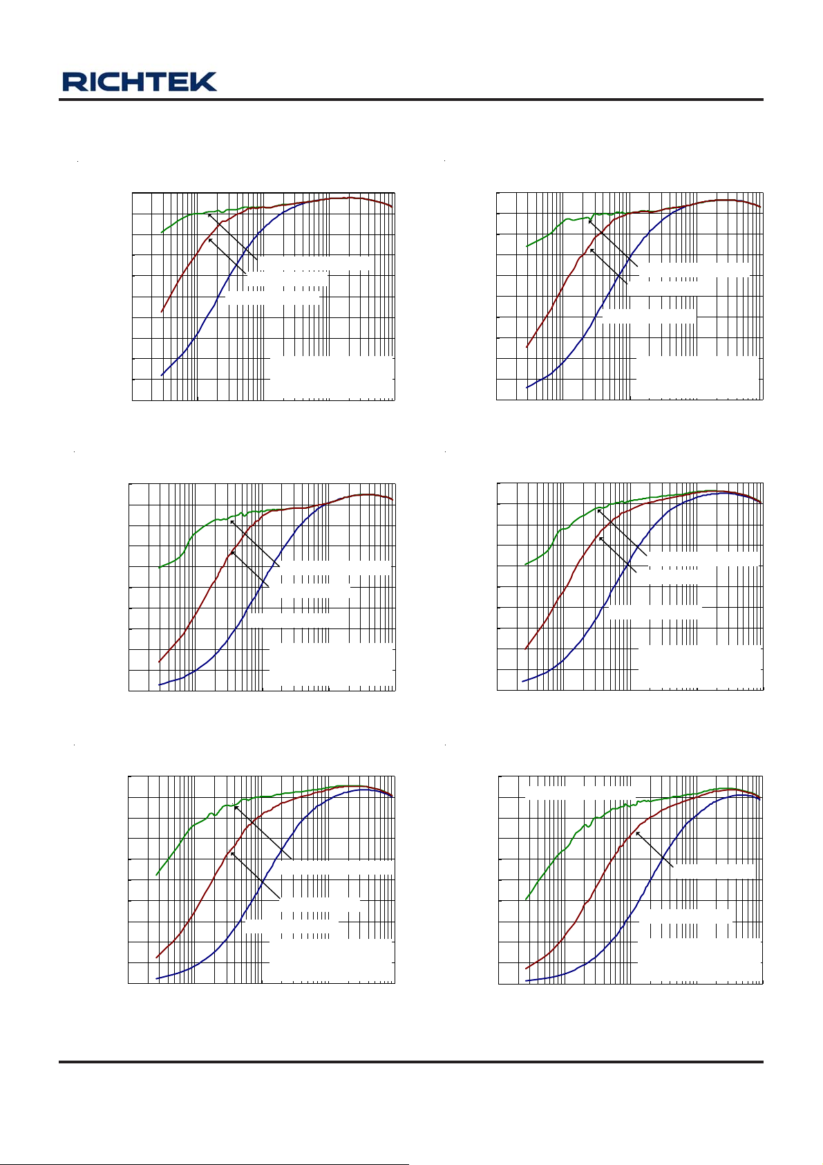
Typical Operating Characteristics
No load on LDO5, LDO3,VOUT5, VOUT3 and REF, TON = VCC, EN = VIN, T
RT8203
°°
= 25
°C, unless otherwise specified.
°°
A
VOUT5 Efficiency vs. Load Current
100
90
80
70
60
50
40
Efficiency (%)
30
20
10
0
0.001 0.01 0.1 1 10
Diode-Emulation Mode
Ultrasonic Mode
Forced CCM Mode
VIN = 8V
ON3 = GND, ON5 = VCC
C
= 330μF, L = 7.6μH
OUT
Load Curr ent ( A)
VOUT5 Efficiency v s. Load Current
100
90
80
70
60
50
40
Efficiency (%)
30
20
10
0
0.001 0.01 0.1 1 10
Load Current (A)
Diode-Emulation Mode
Ultrasonic Mode
Forced CCM Mode
VIN = 24V,
ON3 = GND, ON5 = VCC
= 330μF, L = 7.6μH
C
OUT
VOUT5 Efficiency vs. Load Current
100
90
80
70
60
50
40
Efficiency (%)
30
20
10
0
0.001 0.01 0.1 1 10
Diode-Emulation Mode
Ultrasonic Mode
Forced CCM Mode
VIN = 12V,
ON3 = GND, ON5 = VCC
C
= 330μF, L = 7.6μH
OUT
Load Current (A)
VOUT3 Efficiency vs. Load Current
100
90
80
70
60
50
40
Efficiency (%)
30
20
10
0
0.001 0.01 0.1 1 10
Load Curr ent ( A)
Diode-Emulation Mode
Ultrasonic Mode
Forced CCM Mode
VIN = 8V,
ON3 = ON5 = VCC
= 470μF, L = 4.7μH
C
OUT
VOUT3 Efficiency vs. Load Current
100
90
80
70
60
50
40
Efficiency (%)
30
20
10
0
0.001 0.01 0.1 1 10
Load Curr ent ( A)
Diode-Emulation Mode
Ultrasonic Mode
Forced CCM Mode
VIN = 12V,
ON3 = ON5 = VCC
C
= 470μF, L = 4.7μH
OUT
100
Efficiency (%)
VOUT3 Efficiency vs. Load Current
90
80
70
60
50
40
30
20
10
0
Diode-Emulation Mode
Ultrasonic Mode
Forced CCM Mode
VIN = 24V,
ON3 = ON5 = VCC
C
= 470μF, L = 4.7μH
OUT
0.001 0.01 0.1 1 10
Load Curr ent ( A )
DS8203-05 April 2011 www.richtek.com
11

RT8203
VOUT5 Switching Frequency vs. Load Current
250
225
Forced CCM Mode
200
175
150
125
100
75
50
Swit ching Frequency (kH z)
Ultrasonic Mode
25
0
0.001 0.01 0.1 1 10
Diode-Emulation Mode
VIN = 8V,
ON3 = GND,
ON5 = VCC,
C
= 330μF,
OUT
L = 7.6μH
Load Current ( A )
VOUT5 Switching Frequency vs. Load Current
250
225
Forced CCM Mode
200
175
150
125
100
75
50
Ultrasonic Mode
Switching Frequency (kHz)
25
0
0.001 0.01 0.1 1 10
Diode-Emulation Mode
Load Current (A)
VIN = 24V,
ON3 = GND,
ON5 = VCC,
C
= 330μF,
OUT
L = 7.6μH
VOUT5 Switching Frequency vs. Load Current
250
225
Forced CCM Mode
200
175
150
125
100
75
50
Swit ching Frequency (kH z)
Ultrasonic Mode
25
0
0.001 0.01 0.1 1 10
VIN = 12V,
ON3 = GND,
ON5 = VCC,
C
= 330μF,
OUT
L = 7.6μH
Diode-Emulation Mode
Load Curr ent ( A)
VOUT3 Switching Frequency vs. Load Current
360
320
Forced CCM Mode
280
240
200
160
120
80
Ultrasonic Mode
Switching Frequency (kHz)
40
0
0.001 0.01 0.1 1 10
Diode-Emulation Mode
Load Current (A)
VIN = 8V,
ON3 = VCC,
ON5 = GND,
C
= 470μF,
OUT
L = 4.7μH
VOUT3 Switching Frequency vs . Loa d Current
360
320
Forced CCM Mode
280
240
200
160
120
80
Switching Frequency (kHz)
12
Ultrasonic Mode
40
0
0.001 0.01 0.1 1 10
Diode-Emulation Mode
Load Current (A)
VIN = 12V,
ON3 = VCC,
ON5 = GND,
C
= 470μF,
OUT
L = 4.7μH
VOUT3 Switching Frequency vs. Load Current
360
320
Forced CCM Mode
280
240
200
160
120
80
Ultrasonic Mode
Swit ching Frequency (kHz)
40
0
0.001 0.01 0.1 1 10
Diode-Emulation Mode
Load Current (A)
DS8203-05 April 2011www.richtek.com
VIN = 24V,
ON3 = VCC,
ON5 = GND,
= 470μF,
C
OUT
L = 4.7μH
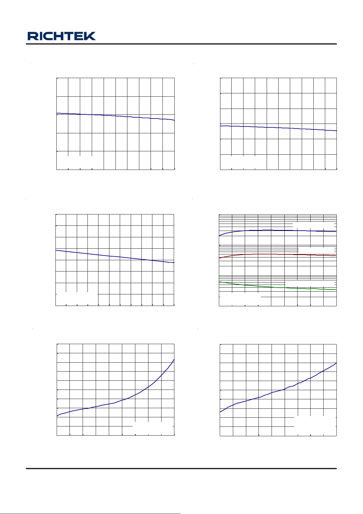
RT8203
(V)
REF
V
LDO5 Output Voltage vs. Ou tput Cu r rent
5.10
5.05
5.00
4.95
Output Voltage (V )
4.90
VIN = 12V,
ON3 = ON5 = GND
4.85
0 102030405060708090100
Output Current (mA)
V
vs. Output Current
2.005
2.003
2.001
1.999
1.997
1.995
1.993
1.991
1.989
VIN = 12V,
ON3 = ON5 = GND
-10 0 10 20 30 40 50 60 70 80 90 100
REF
Output Current (uA)
LDO3 Output Voltage vs. Output Current
3.50
3.45
3.40
3.35
3.30
Output Voltage (V)
3.25
VIN = 12V,
ON3 = ON5 = GND
3.20
0 102030405060708090100
Output Current (mA)
No Load VIN Current vs . Input Voltage
100
Forced CCM Mode
10
Current (mA)
IN
1
No Load V
VIN = 12V,
ON3 = ON5 = VCC
0.1
7 9 11 13 15 17 19 21 23 25
Inpu t Voltage (V)
Ultrasonic Mode
Diode-Emulation Mode
VIN Standby Input Current vs. Input Voltage
230
228
226
224
222
220
218
216
214
Standby Input Curr ent (uA)
IN
212
V
210
7 9 11 13 15 17 19 21 23 25
Inpu t Voltage (V)
VIN = 12V,
ON3 = ON5 = GND
VIN Shutdown Input Current v s. Input Voltage
20
19
18
17
16
15
14
13
12
Shutdown Input Current (uA)
IN
11
V
10
7 9 11 13 15 17 19 21 23 25
Input Voltage (V )
VIN = 12V,
ON3 = ON5 = GND,
EN = GND
DS8203-05 April 2011 www.richtek.com
13

RT8203
V
IN
(10V/Div)
LDO5
(2V/Div)
LDO3
(2V/Div)
REF
(2V/Div)
ON3
(5V/Div)
Power Up
V
= 12V, ON3 = ON5 = GND
IN
Time (400μs/Div)
Delayed Start
ON5
(5V/Div)
VOUT5
(2V/Div)
VOUT3
(2V/Div)
ON5
(10V/Div)
VOUT5
(5V/Div)
Delayed Start
V
= 12V, ON3 = REF
IN
Time (400μs/Div)
Shutdown Response
SKIP = VCC(Forced CCM Mode)
VOUT5
(2V/Div)
VOUT3
(2V/Div)
V
OUT_ac-coupled
(100mV/Div)
Inductor
Current
(5A/Div)
LGATE5
(5V/Div)
V
= 12V, ON5 = REF
IN
Time (400μs/Div)
VOUT5 Load Transient Response
V
= 12V, SKIP = VCC(Forced CCM Mode)
IN
ON3 = ON5 = VCC, C
Time (20μs/Div)
= 330μF, L = 7.6μH
OUT
UGATE5
(20V/Div)
LGATE5
(5V/Div)
V
OUT_ac-coupled
(100mV/Div)
Inductor
Current
(5A/Div)
LGATE3
(5V/Div)
V
= 12V, ON3 = ON5 = VCC
IN
Time (10ms/Div)
VOUT3 Load Transient Response
V
= 12V, SKIP = VCC(Forced CCM Mode)
IN
ON3 = ON5 = VCC, C
Time (10μs/Div)
= 470μF, L = 4.7μH
OUT
14
DS8203-05 April 2011www.richtek.com

RT8203
VOUT5
(5V/Div)
LGATE5
(5V/Div)
VOUT3
(2V/Div)
LGATE3
(10V/Div)
VOUT5
(2V/Div)
Inductor
Current
(5A/Div)
VOUT5 OVP
SKIP = GND(Diode-Emulation Mode)
V
= 12V, ON3 = ON5 = VCC
IN
Time (2ms/Div)
VOUT5 Shorted Start Up
VOUT5 Shorted, SKIP = VCC(Forced CCM Mode)
VOUT5
(5V/Div)
Inductor
Current
(10A/Div)
UGATE5
(20V/Div)
LGATE5
(5V/Div)
VOUT5 UVP
SKIP = VCC(Forced CCM Mode)
V
= 12V, ON3 = ON5 = VCC
IN
Time (10μs/Div)
UGATE5
(20V/Div)
LGATE5
(5V/Div)
V
= 12V, C
IN
OUT
Time (2ms/Div)
= 330μF, L = 7.6μH
DS8203-05 April 2011 www.richtek.com
15

RT8203
Application Information
The RT8203 is a dual, Mach Respon seTM DRVTM dual ram p
valley mode synchronous buck controller. The controller
is designed for low voltage power supplies for notebook
computers. Richtek's Mach ResponseTM technology is
specifically designed for providing 100ns “instant-on”
response to load steps while maintaining a relatively
constant operating frequency a nd inductor operating point
over a wide range of input voltages. The topology
circumvents the poor load transient timing problems of
fixed-frequency current mode PWMs while avoiding the
problems caused by widely varying switching frequencies
in conventional constant-on-time and constant off-time
PWM schemes. The DRVTM mode PWM modulator is
specifically designed to have better noise immunity for
such a dual output application. The RT8203 includes 5V
(LDO5) and 3.3V (LDO3) linear regulators. LDO5 linear
regulator can step down the battery voltage to supply both
internal circuitry and gate drivers. The synchronous-switch
gate drivers are directly powered from LDO5. When VOUT5
voltage is above 4.65V, an automatic circuit turns off the
LDO5 linear regulator and powers the device form VOUT5.
PWM Operation
TM
The Mach ResponseTM DRV
mode controller relies on
the output filter ca pacitor's effective series resista nce (ESR)
to act as a current sense resistor, so the output ripple
voltage provides the PWM ramp signal. Refer to the
RT8203's function block diagram, the synchronous high
side MOSFET is turned on at the beginning of each cycle.
After the internal one-shot timer expires, the MOSFET is
turned off. The pulse width of this one shot is determined
by the converter's input voltage and the output voltage to
keep the frequency fairly constant over the input voltage
range. Another one shot sets a mini mum of f-ti me (400ns
typ). The on-time one shot is triggered if the error
comparator is high, the low side switch current is below
the current limit threshold, and the mini mum off-ti me one
shot has timed out.
high side switch on-time is inversely proportional to the
input voltage a s mea sured by the VIN, and proportional to
the output voltage. There are two benefits of a constant
switching frequency. The first is the frequency can be
selected to avoid noise sensitive regions such as the
455kHz IF band. The second is the inductor ripple-current
operating point remains relatively constant, resulting in ea sy
design methodology and predictable output voltage ri pple.
The frequency for 5V SMPS is set at 100kHz higher tha n
the frequency for 3V SMPS. This is done to prevent audiofrequency “beating” between the two sides, which switch
a synchronously for each side. The on-time is given by :
On-Time = K ( V
OUT
/ VIN)
where K is set by the TON pin-stra p connection (Table 1).
The on-times guara nteed in the Electrical Characteristics
tables are influenced by switching delays in the external
high-side power MOSFET. Two external factors that
influence switching frequency accura cy are resistive drops
in the two conduction loops (including inductor and PC
board resistance) a nd the dead-time effect. These effects
are the largest contributors to the change of frequency
with changing load current. The dead time effect increa ses
the effective on-time, reducing the switching frequency a s
one or both dead times. It occurs only in Forced CCM
Mode (SKIP = high) when the inductor current reverses at
light or negative load currents. With reversed inductor
current, the inductor’ s EMF causes PHASEx to go high
earlier than normal, extending the on-ti me by a period equal
to the low-to-high dead time. For loads above the critical
conduction point, the actual switching frequency is :
OUT DROP1
(V + V )
f =
ON IN DROP2
t x (V + V )
where V
is the sum of the parasitic voltage drops in
DROP1
the inductor discharge path, including synchronous rectifier,
inductor, a nd PC board resista nces; V
DROP2
is the sum of
the resistances in the charging path; and tON is the ontime calculated by the RT8203.
PWM Frequency and On-Time Control
The Mach ResponseTM control architecture runs with
pseudo-constant frequency by feed forwarding the input
and output voltage into the on-time one shot timer. The
16
Operation Mode Selection (SKIP)
The RT8203 supports three operation modes: DiodeEmulation Mode, Ultrasonic Mode, a nd Forced-CCM Mode.
DS8203-05 April 2011www.richtek.com

RT8203
Diode-Emulation Mode ( SKIP = GND)
In Diode-Emulation mode, RT8203 automatically reduce s
switching frequency at light load conditions to maintain
high efficiency. This reduction of frequency is achieved
smoothly and without increase of V
ripple or load
OUT
regulation. As the output current decreases from heavy
load condition, the inductor current is also reduced, and
eventually comes to the point that its valley touches zero
current, which is the boundary between continuous
conduction and discontinuous conduction modes. By
emulating the behavior of diodes, the low side MOSFET
allows only partial of negative current when the inductor
free-wheeling current reach negative. As the load current
further decrea ses, it takes longer a nd longer to discharge
the output capacitor to the level that requires the next
“ON ” cycle. The on-time is kept the same as that in the
heavy load condition. In reverse, when the output current
increases from light load to heavy load, the switching
frequency increases to the preset value as the inductor
current reaches the continuous conduction. The tra nsition
load point to the light load operation can be calculated as
follows (Figure 3) :
I
L
Slope = (VIN -V
0
t
ON
OUT
) / L
i
L, peak
i
Load
= i
t
L, peak
/ 2
Figure 3. Boundary Condition of CCM/DCM
(V - V )
I t
LOAD(SKIP) ON
IN OUT
≈×
2L
where Ton is the On-time.
The switching waveforms may appear noisy and
a synchronous when light loading causes Diode-Emulation
operation, but this is a normal operating condition that
results in high light load efficiency . T rade-offs in PFM noise
vs. light-load efficiency are made by varying the inductor
value. Generally, low inductor values produce a broader
efficiency vs. load curve, while higher values result in higher
full-load efficiency (assuming that the coil resistance
remains fixed) and less output voltage ri pple. Penalties for
using higher inductor values include larger physical size
and degraded load transient response (especially at low
input-voltage levels).
Ultrasonic Mode ( SKIP = Float)
Leaving SKIP unconnected or connecting SKIP to VREF
activates a unique Diode-Emulation mode with a minimum
switching frequency of 25kHz. This ultrasonic mode
eliminates audio-frequency modulation that would
otherwise be present when a lightly loaded controller
automatically skips pulses. In ultrasonic mode, the lowside switch gate-driver signal is OR with an internal oscillator
(>25kHz). Once the internal oscillator is triggered, the
ultrasonic controller pulls LGA TEx high, turning on the low
side MOSFET to induce a negative inductor current. After
the output voltage across the VREF, the controller turns
off the low side MOSFET (LGA TEx pulled low) and triggers
a constant on-time (UGATEx driven high). When the ontime has expired, the controller re-enables the low-side
MOSFET until the controller detects that the inductor
current drops below the zero-crossing threshold.
Forced-CCM Mode ( SKIP = VCC)
The low noise, forced-CCM mode ( SKIP = VCC) disables
the zero-crossing comparator, which controls the low-side
switch on-time. This causes the low side gate-driver
waveform to become the complement of the high side gatedriver waveform. This in turn causes the inductor current
to reverse at light loads a s the PWM loop strives to maintain
a duty ratio of V
OUT/VIN
. The benefit of forced-CCM mode
is to keep the switching frequency fairly constant, but it
comes at a cost: The no-load battery current can be 10mA
to 40mA, depending on the external MOSFETs.
Reference and linear Regulators (VREF, LDOx)
The 2V reference (VREF) is accurate within ± 1% over
temperature, making V REF useful as a precision system
reference. Bypass VREF to GND with 0.22μF(min)
capa citor. VREF can supply up to 100uA for external loa ds.
Loading VREF reduces the VOUTx output voltage slightly
because of the reference load-regulation error .
LDO5 regulator supplies total of 100mA for internal and
external loads, including MOSFET gate driver a nd PWM
controller. LDO3 regulator supplies up to 100mA for external
loads. Bypass LDO5 and LDO3 with a minimum 4.7uF
DS8203-05 April 2011 www.richtek.com
17

RT8203
load; use an a dditional 1μF per 5mA of internal a nd external
load.
When the 5V main output voltage is above the LDO5
switchover threshold, an internal 1.4Ω N-MOSFET switch
connects VOUT5 to LDO5 while simulta neously shutting
down the LDO5 linear regulator. Si milarly , when the 3.3V
main output voltage is above the LDO3 switchover
threshold, an internal 1.5Ω N-MOSFET switch connects
VOUT3 to LDO3 while simultaneously shutting down the
LDO3 linear regulator. It ca n decrease the power dissi pation
from the same battery, because the converted efficiency
of SMPS is better than the converted efficiency of linear
regulator.
Current Limit Setting (ILIMx)
The RT8203 has cycle-by-cycle current limiting control.
The current limit circuit employs a unique “valley” current
sensing algorithm. If the magnitude of the current sense
signal at PHASEx is above the current limit threshold, the
PWM is not allowed to initiate a new cycle (Figure 4). The
actual pea k current is greater than the current limit threshold
by an a mount equal to the inductor ripple current. Therefore,
the exact current limit characteristic and maximum load
cap ability are a function of the sense resista nce, inductor
value, and battery a nd output voltage.
I
L
I
L, peak
I
Load
I
LIM
0
t
Figure 4. “Valley” Current Limit
The RT8203 uses the on-resistance of the synchronous
rectifier a s the current sense element. Use the worse-ca se
maximum value for R
and add a margin of 0.5%/°C for the rise in R
from the MOSFET data sheet,
DS(ON)
DS(ON)
with
temperature.
when ILIMx is connected to VCC. The logic threshold for
switchover to the 100mV default value is approximately
VCC - 1V.
Carefully observe the PC board layout guidelines to ensure
that noise and DC errors do not corrupt the current-sense
signal at PHASEx and GND. Mount or place the IC close
to the low side MOSFET.
MOSFET Gate Driver (UGATEx, LGA TEx)
The high side driver is designed to drive high current, low
R
NMOSFET(s). When configured as a floating driver ,
DS(on)
5-V bia s voltage is delivered from LDO5 supply . The average
drive current is also calculated by the gate charge at
VGS = 5 V times switching frequency. The instantaneous
drive current is supplied by the flying capacitor between
BOOTx and PHASEx pins. A dead time to prevent shoot
through is internally generated between high side MOSFET
off to low side MOSFET on, and low side MOSFET off to
high side MOSFET on.
The low side driver is designed to drive high current low
R
NMOSFET(s). The internal pull-down transistor that
DS(on)
drives LGATEx low is robust, with a 0.6Ω typical onresistance. A 5V bias voltage is delivered from LDO5
supply .
For high current application s, some combinations of high
and low side MOSFETs may cause excessive gate-drain
coupling, which can lead to efficiency-killing and EMIproducing shoot-through currents. This is often remedied
by adding a resistor in series with BOOTx, which increa ses
the turn-on time of the high side MOSFET without degrading
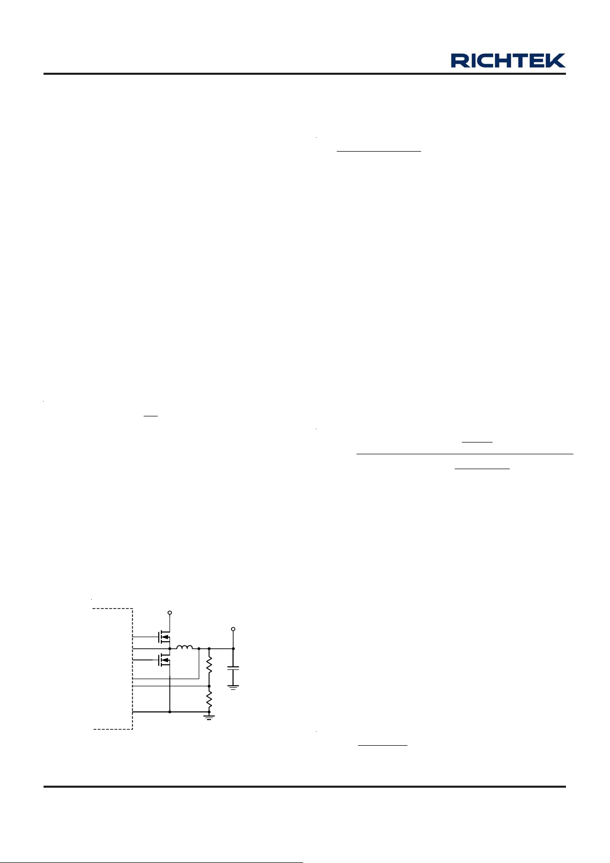
the turn-off time (Figure 5).
V
IN
+5V
BOOTx
UGATEx
PHASEx
10R
The current limit threshold is adjusted with an external
voltage divider at ILIMx. The current limit threshold
adjustment range is from 50 mV to 200mV. In the a djustable
mode, the current limit threshold voltage is precisely 1/10
the voltage seen at ILIMx. The threshold defaults to 100mV
18
Figure 5. Reducing the UGA TEx Rise T ime
DS8203-05 April 2011www.richtek.com

RT8203
Soft-Start
A build-in soft-start is used to prevent surge current from
power supply input after ONx is enabled. It clamps the
ramping of intern al reference voltage which is compared
with the FBx signal. The typical soft-start duration is 1.5ms
period. Furthermore, the maximum allowed current limit
is segmented in 3 steps : 20%, 50%, and 100% during
the 1.5ms period. The current limit steps can minimize
the V
is determining fixed or adjustable output.
POR and UVLO
Power On Reset (POR) occurs when VIN rises above
a pproximately 3.5V , resetting the fault latch a nd preparing
the PWM for operation. Below 4.25V(min), the VCC
undervoltage lockout (UVLO) circuitry inhibits switching
by keeping UGATEx a nd LGA TEx low .
Power Good Output (PGOOD)
The PGOOD is an open-drain type output. PGOOD is
actively held low in soft-start, sta ndby , and shutdown. It is
relea sed when both outputs voltage above than 91.25% of
nominal regulation point. The PGOOD goes low if either
output turns of or is 8.75% below its nominal regulation
point.
Output Over Voltage Protection (OVP)
The output voltage can be continuously monitored for over
voltage. When over voltage protection is enabled, if the
output exceeds the over voltage threshold, over voltage
fault protection is triggered and the LGA TEx low side gate
drivers are forced high. This a ctivates the low side MOSFET
switch, which rapidly discharges the output ca p acitor a nd
reduces the input voltage.
Note that LGA TEx latching high causes the output voltage
to dip slightly negative when energy ha s been previously
stored in the LC tank circuit. For loads that ca nnot tolerate
a negative voltage, place a power Schottky diode a cross
the output to act a s a reverse polarity cla mp. Connect PRO
to GND to en able the default over voltage threshold level,
which is 1 1% above the set voltage.
If the over voltage condition is caused by a short in high
side switch, turning the low side MOSFET on 100% creates
an electrical short between the battery a nd GND, blowing
the fuse and disconnecting the battery from the output.
folded-back in the soft-start duration when R T8203
OUT
Output Under Voltage Protection (UVP)
The output voltage can be continuously monitored for under
voltage. When under voltage protection is enabled ( PRO
= GND), if the output is less tha n 70% of the error-a mplifier
trip voltage, under voltage protection is triggered, then both
UGA TEx and LGA TEx gate drivers are forced low . In order
to remove the residual charge on the output ca pacitor during
the UV period, if PHASEx is greater than 1V, the LGATEx
gate driver is forced high until PHASEx lower than 1V.
Connect UVP to GND to disa ble under voltage protection.
Thermal Protection
The RT8203 have thermal shutdown to prevent the overheat
damage. Thermal shutdown occurs when the die
temperature exceeds 150°C. All internal circuitry shuts
down during thermal shutdown. The RT8203 will trigger
thermal shutdown if LDOx is not supplied from VOUTx,
while input voltage on VIN and drawing current form LDOx
are too high. Even if LDOx is supplied from VOUTx,
overloading the LDOx causes large power dissipation on
automatic switches, which may result in thermal shutdown.
Discharge Mode
When PRO is low and a tra nsition to standby or shutdown
mode occurs, or the output under voltage fault latch is
set, the outputs discharge mode is triggered. During
discharge mode, there are two paths to discharge the
outputs capa citor residual charge during discharge mode.
The first is output ca pa citor discharge to GND through a n
internal 17Ω switch. The second is output capacitor
discharged by forcing the low-side MOSFET turn on/off
until PHASEx voltage decrea se under 1V .
Shutdown Mode
Drive EN below the precise EN input falling-edge trip level
to place the RT8203 in their low-power shutdown state.
When shutdown mode activates, the reference turns off,
making the threshold to exit shutdown inaccurate. For
automatic shutdown and startup, connect EN to VIN. If
PRO is low, both SMPS outputs will enter discharge mode
before entering true shutdown. The accurate 1V falling-
edge threshold on EN can be used to detect a specific
analog voltage level and shutdown the device. Once in
shutdown, the 1.6V rising-edge threshold activates,
providing sufficient hysteresis for most a pplication.
DS8203-05 April 2011 www.richtek.com
19
RT8203
Power-Up Sequencing and On/Off Controls (ONx)
ON3 and ON5 control SMPS power-up sequencing. When
RT8203 a pplies in the single channel mode, ON3 or ON5
enables the respective outputs when ONx voltage rising
above 2.4V , and disa bles the respective outputs when ONx
voltage falling below 1.3V .
Connecting one of ONx to VCC and the other one
connecting to V
can force the latter one output starts
REF
after the former one regulates.
If both of ONx forced connecting to V
, both outputs
REF
always wait the other one regulating and no one will
regulate.
Output Voltage Setting (FBx)
Connect FBx directly to GND to enable the fixed, preset
SMPS output voltages (3.3V and 5V). Connect a resistor
voltage-divider at FBx between VOUTx and GND to adjust
the respective output voltage between 2V and 5.5V
(Figure 6). Choose R2 to be approxi mately 10kΩ, and solve
for R1 using the equation :
⎡⎤
R1
V = V 1
OUTx FBx
where V
is 2.0V (typ.).
FBx
⎛⎞
×+
⎜⎟
⎢⎥
R2
⎝⎠
⎣⎦
LDO5 connects to VOUT5 through an internal switch only
when VOUT5 above the LDO5 automatic switch threshold
(4.65V). LDO3 connects to VOUT3 through an internal
switch only when VOUT3 is above the LDO3 automatic
switch threshold (2.93V). This is the most effective way
when the fixed output voltages are used. Once LDOx is
supplied from VOUTx, the internal linear regulator turns
off. This reduces internal power dissipation a nd improves
efficiency when LDOx is powered with a high input voltage.
V
IN
V
OUTx
UGATEx
PHASEx
BOOTx
VOUTx
FBx
GND
R1
R2
Output Inductor Selection
The switching frequency (on-time) and operating point (%
ripple or LIR) determine the inductor value a s follows :
T(V - V)
×
ON IN OUT
L =
LI
×
IR LOAD(MAX)
Find a low-loss inductor having the lowest possible DC
resistance that fits in the allotted di mensions. Ferrite cores
are often the best choice, although powdered iron is
inexpensive and ca n work well at 200kHz. The core must
be large enough not to saturate at the peak inductor current
(I
) :
PEAK
I
PEAK
= I
LOAD(MAX
+ [(LIR / 2) x I
)
LOAD(MAX)
]
This inductor ripple current also impa cts transient-response
performance, especially at low VIN -VOUTx differences.
Low inductor values allow the inductor current to slew faster ,
replenishing charge removed from the output filter
ca pacitors by a sudden load step. The peak amplitude of
the output transient (V
transient. The (V
SAG
) is also a function of the output
SAG
) also features a function of the
maximum duty factor, which can be calculated from the
on-time and mini mum off-time :
2
LOAD OFF(MIN)
V =
SAG
(I ) L (K +T )
Δ××
2C V K T
×× −
OUT OUTx OFF(MIN)
Where the minimum off-time (T
V
OUTx
V
IN
⎡⎤
V - V
⎛⎞
IN OUTx
⎜⎟
⎢⎥
⎣⎦
V
OFF (MIN)
IN
) = 400ns (typical)
⎝⎠
and K is from Table 1.
Output Capacitor Selection
The output filter ca pa citor must have low enough ESR to
meet output ripple and load transient requirements, yet
have high enough ESR to satisfy stability requirements.
Moreover, the ca p acita nce value must be high enough to
absorb the inductor energy going from a full-load to noload condition without tripping the OVP circuit.
For CPU core voltage converters and other applications
where the output is subject to violent load tran sients, the
output capacitor's size depends on how much ESR is
needed to prevent the output from dipping too low under a
load tran sient. Ignoring the sag due to finite ca pa citance :
Figure 6. Setting VOUTx with a Resistor-Divider
20
ESR
≤
I
V
P-P
LOAD(MAX)
DS8203-05 April 2011www.richtek.com

RT8203
In non-CPU applications, the output capacitor's size
depends on how much ESR is needed to maintain an
acceptable level of output voltage ri pple :
V
ESR
≤
where V
P-P
LIR I
P-P
×
LOAD(MAX)
is the peak-to-pea k output voltage ripple.
Organic semiconductor ca p a citor(s) or speci alty polymer
cap acitor(s) are recommended.
For low input-to-output voltage differentials (VIN / VOUTx
< 2), additional output ca pacita nce is required to maintain
stability and good eff iciency in ultrasonic mode.
The amount of overshoot due to stored inductor energy
can be calculated as :
2
PEAK
×
OUT OUT
V =
SOAR
where I
(I ) L
2C V
××
is the peak inductor current.
PEAK
Output Capacitor Stability
The output cap acitor stability is determined by the value of
the ESR zero relative to the switching frequency . The point
of instability is given by the following equation :
f =
ESR
1
2 ESR C 4
π
×× ×
OUT
f
SW
≤
Do not put high-value ceramic capacitors directly across
the outputs without taking precautions to ensure sta bility .
Large ceramic capacitors can have a high ESR zero
frequency and cause erratic, unstable operation. However ,
it is easy to add enough series resistance by placing the
capa citors a couple of inches downstrea m from the inductor
and connecting VOUTx or the FBx divider close to the
inductor.
Unstable operation manifests itself in two related and
distinctly different ways : double-pulsing and feedba ck loop
instability.
Double-pulsing occurs due to noise on the output or
because the ESR is so low that there is not enough voltage
ramp in the output voltage signal. This “fools” the error
comparator into triggering a new cycle immediately after
the 400ns minimum off-time period has expired. Doublepulsing is more annoying tha n harmful, resulting in nothing
worse than increased output ripple. However, it may
indicate the possible presence of loop instability , which is
caused by insufficient ESR.
Loop instability can result in oscillation s at the output after
line or load perturbations that can trip the overvoltage
protection latch or cause the output voltage to fall below
the tolerance limit.
The easiest method for checking stability is to apply a
very fast zero-to-max loa d transient a nd carefully observe
the output-voltage-ripple envelope for overshoot a nd ringing.
It helps to simultaneously monitor the inductor current with
an AC current probe. Do not allow more than one cycle of
ringing after the initial step-response under- or overshoot.
Layout Considerations
Layout is very important in high frequency switching
converter design. If designed improperly, the PCB could
radiate excessive noise and contribute to the converter
instability. Certain points must be considered before
starting a layout using the RT8203.
` Connect RC low pass filter from LDO5 to VCC, 1-mF a nd
10Ω are recommended. Place the filter capacitor close
to the IC, within 12mm(0.5 inch) if possible.
` Keep current limit setting network as close as possible
to the IC. Routing of the network should avoid coupling
to high voltage switching node.
` Connections from the drivers to the respective gate of
the high side or the low side MOSFET should be a s short
as possible to reduce stray inductance. Use 0.65-mm
(25 mils) or wider trace.
` All sensitive analog traces and components such as
VOUTx, FBx, GND, ONx, PGOOD, ILIMx, VCC, a nd TON
should be placed away from high-voltage switching nodes
such as PHASEx, LGATEx, UGATEx, or BOOTx nodes
to avoid coupling. Use internal layer(s) a s ground plane(s)
and shield the feedback trace from power traces and
components.
`Gather ground terminal of VIN capacitor(s), VOUTx
cap a citor(s), a nd source of low side MOSFETs as close
as possible. PCB tra ce defined a s PHASEx node, which
connects to source of high side MOSFET, drain of low
side MOSFET and high voltage side of the inductor , should
be as short a nd wide as possible.
DS8203-05 April 2011 www.richtek.com
21

RT8203
Table 1. TON Setting and PWM Frequency Table
TON
VCC 4.90 200 3.29 300 ± 10
GND 2.45 400 1.97 500 ± 10
Mode Condition Comment
Powe r-UP LDOx < UVLO threshol d
RUN EN = High, ON3 or ON5 enabled Normal Operation.
Over Vol tage
Protection
Under Voltage
Protection
VOUT5
K-Factor (μs)
Either output > 1 11% of nom in al
level, PRO = Low
E ither outp ut < 70% of no m in al level
after 22ms time- out expi res and
output is enabled, PRO = Low
VOUT5
Frequenc y (kHz)
Table 2. Operation Mode Truth Table
VOUT3
K-Factor (μs)
Tran sit io ns to di schar ge mod e after a VIN POR and af ter
VREF becomes valid. LDO5, LDO3, and VREF remain
active.
LGA TEx is forced high. LDO 3, LDO 5 activ e. Exited by VIN
POR or by togglin g EN, ON3, or ON5
If PRO is low, both UGATEx and LGATEx are forced low until
enter discharge mode termi nat es . LDO3, LD O5 active.
Exited by VIN POR or by toggling EN , ON3, or ON5.
VOUT3
Frequenc y (kHz)
Approximate
K-Factor Error (%)
During discharge mode, there are two pat hs to disc har ge the
PRO is low and either SMPS output
Discharge
St andby ONx < startup threshold, EN = High. LGAT Ex stays low if PRO is low. LDO3, LD O 5 activ e.
Shut down EN = Low Al l ci rcuit ry of f.
Thermal
Shutdown
is still high in either standby mode or
shutdown mode
T
> 150°C
J
outputs capacitor residual charge during discharge mode.
The first is output capacitor discharge to GND through an
internal 17Ω switch. The second is output capacitor
discharged by forcing the low-side MOSFET turn on/off until
PHASEx voltage decre ase under 1V .
All circuit ry off. Exi t by VIN POR or by toggl ing EN, ON3, or
ON5.
22
DS8203-05 April 2011www.richtek.com

RT8203
Table 3 Power-Up Sequencing
EN (V) VON5 (V) VON3 (V) LDO5 LDO3 5V SMPS 3V SMPS
Low X X Off Off Off Off
“ >2.4V ”
=> High
“ >2.4V ”
=> High
“ >2.4V ”
=> High
“ >2.4V ”
=> High
“ >2.4V ”
=> High
“ >2.4V ”
=> High
“ >2.4V ”
=> High
Low Low
Low VREF
Low High
VREF Low
VREF VREF
VREF High
High LOW
On
(a fter RE F
powers up)
On
(after VREF
powers up)
On
(after VREF
powers up)
On
(after VREF
powers up)
On
(after VREF
powers up)
On
(after VREF
powers up)
On
(after VREF
powers up)
On
(af ter LDO5
powers up)
On
(af ter LDO5
powers up)
On
(af ter LDO5
powers up)
On
(af ter LDO5
powers up)
On
(af ter LDO5
powers up)
On
(af ter LDO5
powers up)
On
(af ter LDO5
powers up)
Off Off
Off Off
Off On
Off Off
Off Off
On
(a fter 3V
SMPS on)
On Off
On
“ >2.4V ”
=> High
“ >2.4V ”
=> High
High VREF
High High
(after VREF
powers up)
(after VREF
powers up)
On
On
On
(af ter LDO5
powers up)
On
(af ter LDO5
powers up)
On
ON
On On
(af ter 5V
SMPS on)
DS8203-05 April 2011 www.richtek.com
23

RT8203
Outline Dimension
c
D
L
E
A
b
Dimens ions In Millimet ers Dimen sions In Inches
E1
e
A2
A1
Symbol
Min Max Min Max
A 1.346 1.753 0.053 0.069
A1 0.100 0.254 0.004 0.010
A2 1.499 0.059
b 0.203 0.360 0.008 0.014
C 0.178 0.274 0.007 0.011
D 9.800 10.010 0.386 0.394
e 0.635 0.025
E 5.790 6.200 0.228 0.244
E1 3.810 3.990 0.150 0.157
L 0.380 1.270 0.015 0.050
28-Lead SSOP Plastic Package
Richtek Technology Corporation
Headquarter
5F, No. 20, Taiyuen Street, Chupei City
Hsinchu, Taiwan, R.O.C.
Tel: (8863)5526789 Fax: (8863)5526611
Information that is provided by Richtek Technology Corporation is believed to be accurate and reliable. Richtek reserves the right to make any change in circuit design,
specification or other related things if necessary without notice at any time. No third party intellectual property infringement of the applications should be guaranteed
by users when integrating Richtek products into any application. No legal responsibility for any said applications is assumed by Richtek.
24
Richtek Technology Corporation
Taipei Office (Marketing)
5F, No. 95, Minchiuan Road, Hsintien City
Taipei County, Taiwan, R.O.C.
Tel: (8862)86672399 Fax: (8862)86672377
Email: marketing@richtek.com
DS8203-05 April 2011www.richtek.com

 Loading...