

Richtek RT9012-FMPQV, RT9012-FMPQW, RT9012-FSPQW, RT9012-GMPQV, RT9012-GMPQW Schematic [ru]
...
300mA Dual LDO Regulator with POR
RT9012
General Description
RT9012 is a dual channel, low noise, and low dropout with
the sourcing ability up to 300mA and power-on reset
function. The range of output voltage is from 1.2V to 3.6V
by operating from 2.5V to 5.5V input.
The RT9012 offers 2% accuracy, extremely low dropout
voltage (240mV @ 300mA), and extremely low ground
current, only 27uA per LDO. The shutdown current is near
zero current which is suitable for battery-power devices.
Other features include current limiting, over temperature,
output short circuit protection.
The RT9012 is short circuit thermal folded back protected.
The IC lowers its OTP trip point from 165°C to 110°C when
output short circuit occurs (VOUT < 0.4V) providing
maximum safety to end users.
The RT9012 can operate stably with very small ceramic
output capacitors, reducing required board space and
component cost. The RT9012 is available in fixed output
voltages in the
WDFN-8L 2x2 package.
Ordering Information
RT9012-
Package Type
QW : WDFN-8L 2x2 (W-Type)
Features
z Wide Operating Voltage Ranges : 2.5V to 5.5V
z Low-Noise for RF Application
z No Noise Bypass Capa citor Required
z Fast Response in Line/Load Transient
z TTL-Logic-Controlled Shutdown Input
z Low Temperature Coefficient
zz
z Dual LDO Outputs (300mA/300mA)
zz
zz
z Ultra-low Quiescent Current 27uA/LDO
zz
zz
z High Output Accuracy 2%
zz
zz
z Short Circuit Protection
zz
zz
z Thermal Shutdown Protection
zz
zz
z Current Limit Protection
zz
zz
z Short Circuit Thermal Folded Back Protection
zz
zz
z Tiny 8-Lead WDFN Package
zz
zz
z RoHS Compliant and 100% Lead (Pb)-Free
zz
Applications
zz
z CDMA/GSM Cellular Handsets
zz
zz
z Battery-Powered Equipment
zz
zz
z Laptop, Palmtops, Notebook Computers
zz
zz
z Hand-Held Instruments
zz
zz
z PCMCIA Cards
zz
zz
z Portable Information Appliances
zz
Lead Plating System
P : Pb Free
G : Green (Halogen Free and Pb Free)
Output Voltage : VOUT1/VOUT2
VOUT2 > VOUT1 is Recommended
Note :
Pin Configurations
(TOP VIEW)
1
VIN
2
EN1
3
EN2
4
SET
WDFN-8L 2x2
8
VOUT1
7
VOUT2
POR
6
9
5
GND
Richtek products are :
` RoHS compliant and compatible with the current require-
ments of IPC/JEDEC J-STD-020.
` Suitable for use in SnPb or Pb-free soldering processes.
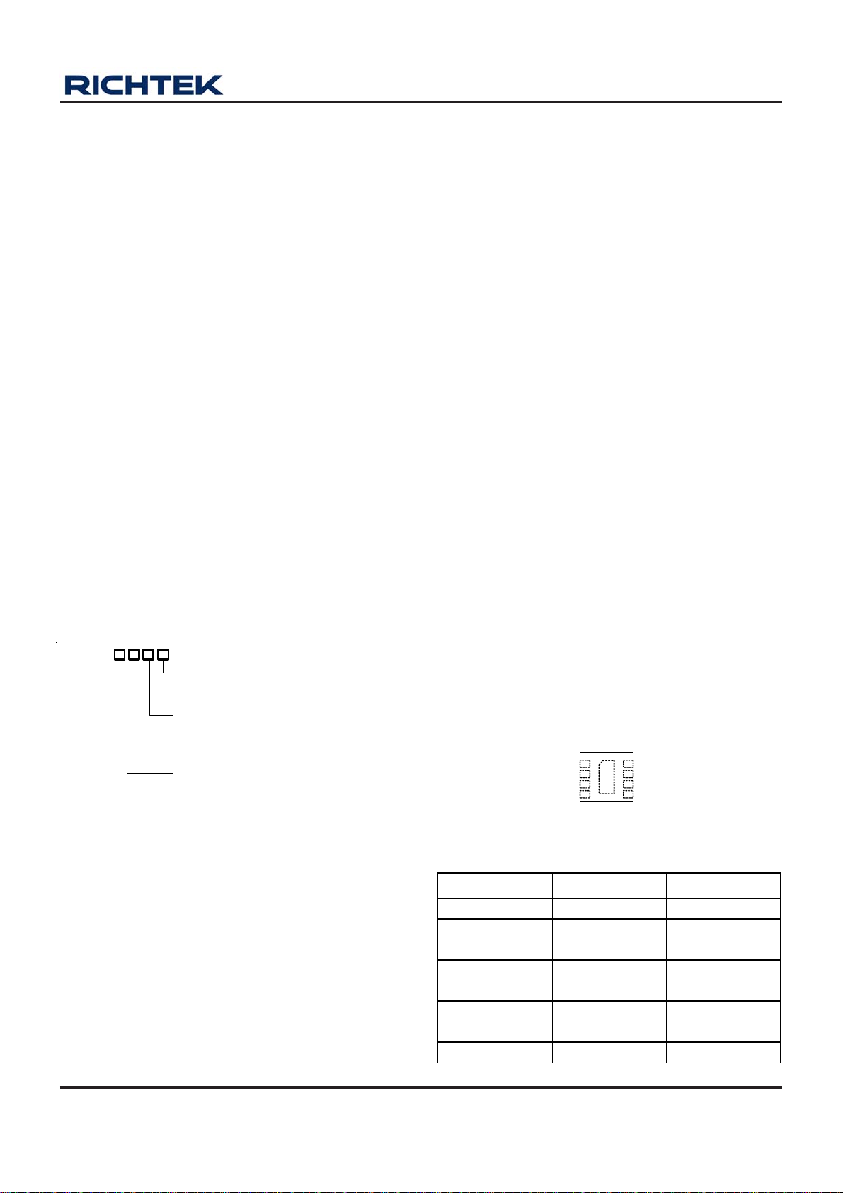
Marking Information
For marking information, contact our sales representative
directly or through a Richtek distributor located in your
area.
Available Voltage Version
Code Voltage Code Voltage Code Voltage
A 3.5 B 1.3 C 1.2
D 1.85 E 2.1 F 1.5
G 1.8 H 2 J 2.5
K 2.6 L 2.7 M 2.8
N 2.85 P 3 Q 3.1
R 3.2 S 3.3 T 2.65
V 2.9 W 1.6 X 3.15
Y 1.9
DS9012-09 April 2011 www.richtek.com
1
RT9012
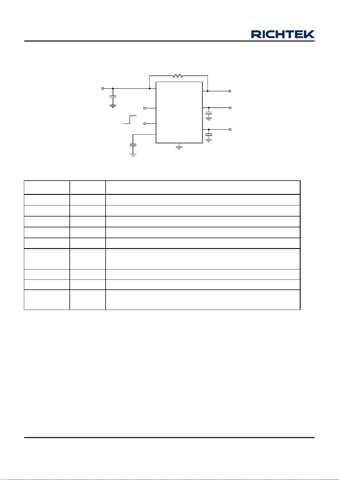
Typical Application Circuit
100K
V
IN
C
IN
1uF
Chip Enable
C
DELAY
VIN
EN1
EN2
SET
RT9012
VOUT1
VOUT2
GND
Functional Pin Description
Pin No. Pin Na me P in Func tion
1 VIN Supply Input.
2 EN1 Chip Enable1 (Active High).
3 EN2 Chip Enable2 (Active High).
4 SET Delay Set Input. Connect external capacitor to GND to set the internal delay.
5 GND Common Ground.
POR
C
OUT1
1uF
C
OUT2
1uF
V
V
OUT1
OUT2
6 POR
7 VOUT2 Channel 2 Output Voltage.
8 VOUT1 Channel 1 Output Voltage.
9 (Exposed Pad) GND
Power-On Reset Output : Open-drain output. Active low indicates an output
under-voltage condition on regulator 2.
The exposed pad must be soldered to a large PCB and connected to GND
for maximum power dissipation.
DS9012-09 April 2011www.richtek.com
2
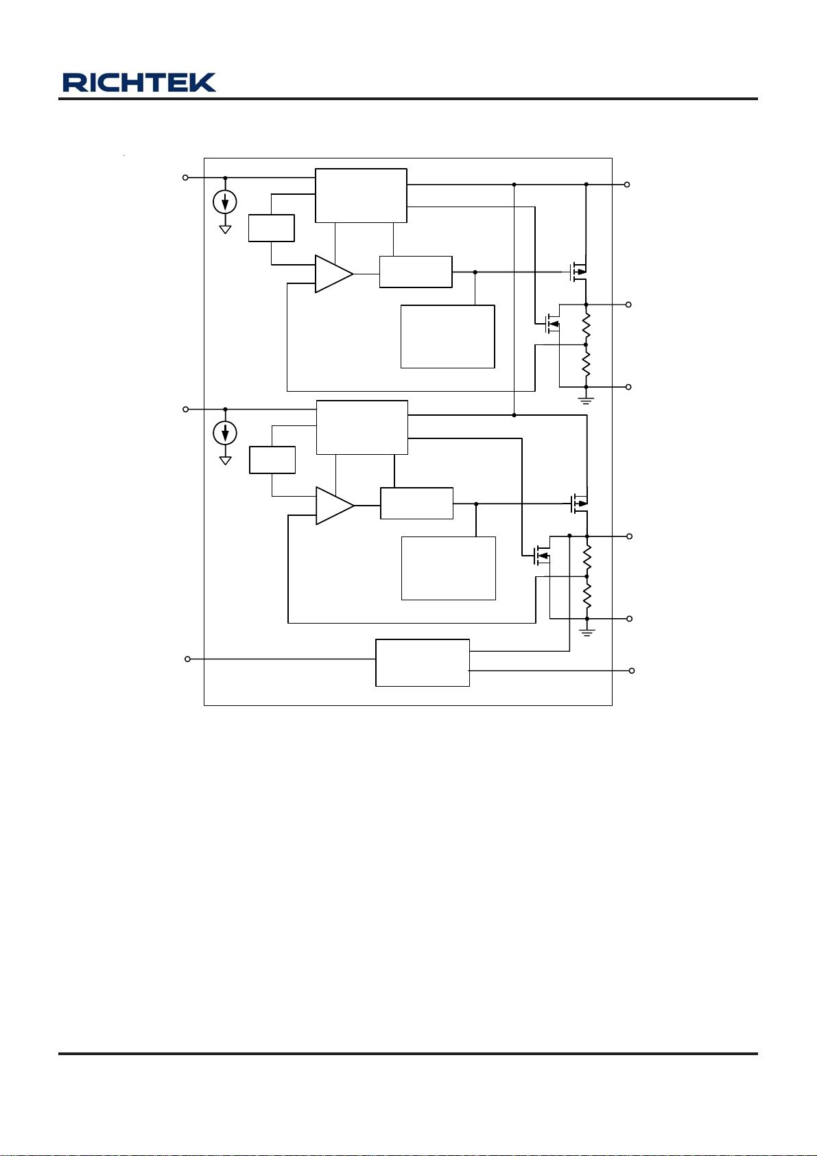
Function Block Diagram
RT9012
EN1
EN2
0.2uA
0.2uA
Shutdown
and
Logic Control
V
REF
-
+
Error
Amplifier
Shutdown
Logic Control
V
REF
-
+
Error
Amplifier
MOS Driver
Current-Limit
and
Thermal
Protection
and
MOS Driver
Current-Limit
and
Thermal
Protection
VIN
VOUT1
GND
VOUT2
SET
POR& Delay
GND
POR
DS9012-09 April 2011 www.richtek.com
3
RT9012
Absolute Maximum Ratings (Note 1)
z Supply Input Voltage ------------------------------------------------------------------------------------------------------ 6V
z Other I/O Pin Voltages --------------------------------------------------------------------------------------------------- 6V
z Power Dissipation, P
WDFN-8L 2x2 -------------------------------------------------------------------------------------------------------------- 0.606W
z Package Thermal Resistance (Note 2)
WDFN-8L 2x2, θJA--------------------------------------------------------------------------------------------------------- 165°C/W
z Junction Temperature ----------------------------------------------------------------------------------------------------- 150°C
z Lead Temperature (Soldering, 10 sec.) ------------------------------------------------------------------------------- 260°C
z Storage Temperature Range -------------------------------------------------------------------------------------------- −65°C to 150°C
z ESD Susceptibility (Note 3)
HBM (Human Body Mode) ---------------------------------------------------------------------------------------------- 2kV
MM (Machine Mode) ------------------------------------------------------------------------------------------------------ 200V
Recommended Operating Conditions (Note 4)
z Supply Input Voltage ------------------------------------------------------------------------------------------------------ 2.5V to 5.5V
z Enable Input Voltage ------------------------------------------------------------------------------------------------------ 0V to 5.5V
z Operation Junction Temperature Range ------------------------------------------------------------------------------ −40°C to 125°C
z Operation Ambient Temperature Range ------------------------------------------------------------------------------ −40°C to 85°C
@ T
D
= 25°C
A
Electrical Characteristics
(V
= V
OUT
+ 1V, V
IN
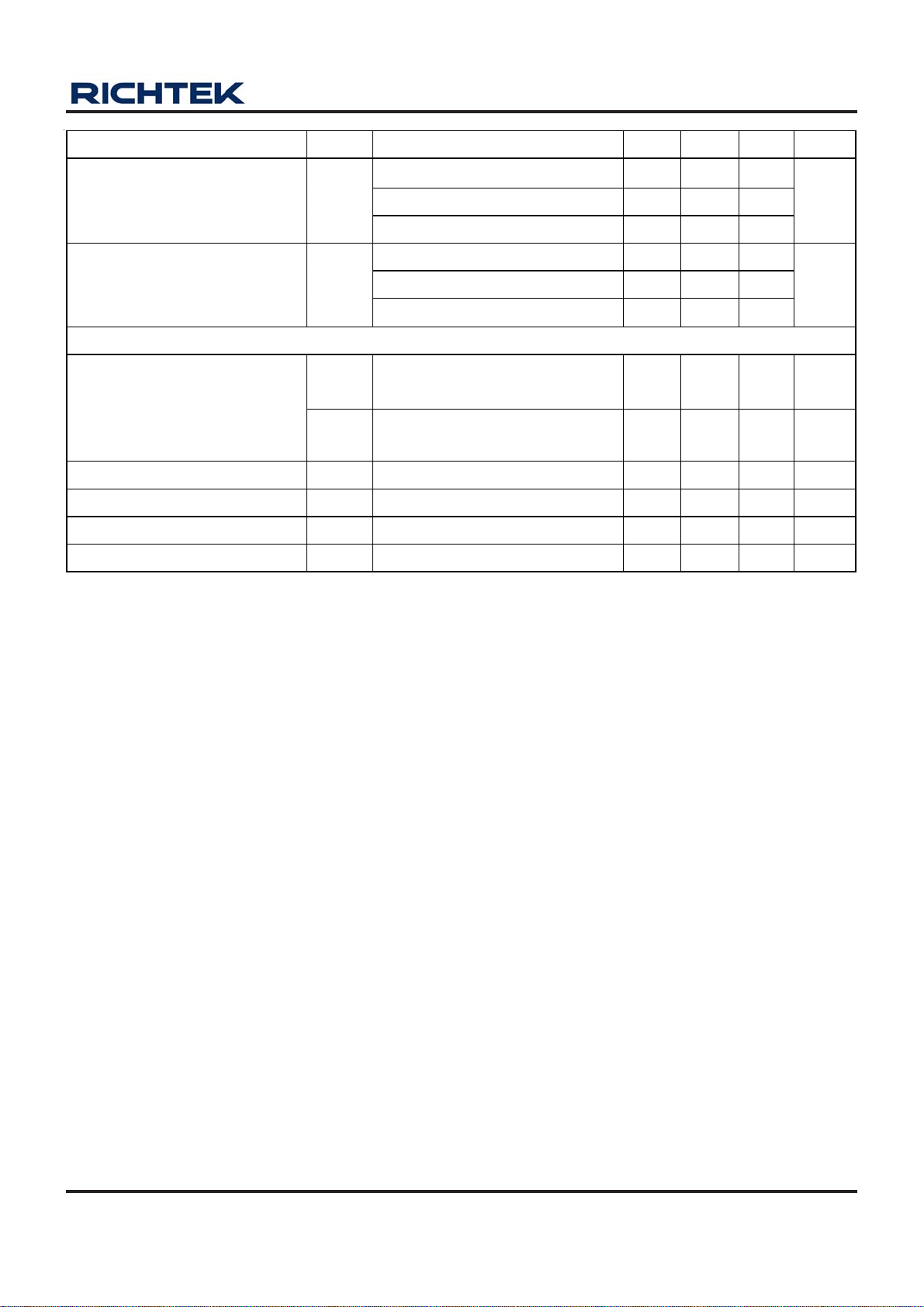
Parameter Symbol Test Conditions Min Typ Max Unit
Input Voltage
Dropout Voltage (Note 5)
Output voltage range
V
Accuracy
OUT
Line Regulation
Load Regulation
Current Limit
Quiescent Current
Shutdown Current
EN Threshold
Output Voltage TC -- 100 -- ppm/°C
= VIN, C
EN
= C
IN
= 1μF, TA = 25°C, unless otherwise specified.)
OUT
V
V
IN
V
DROP
V
OUT
ΔV
ΔV
LINE
ΔV
LOA D
I
VEN > 1.5V
Q
I
VEN < 0.4V
Q_SD
VIH V
V
V
IL
= 2.5V to 5.5V
IN
I
= 150mA
OU T
= 300mA
I
OU T
1.2 -- 3.6 V
I
= 1mA
OU T
V
= (V
IN
> 2.5V, whichever is larger
V
IN
1mA < I
R
LOA D
= 2.5V to 5.5V, Power On
IN
= 2.5V to 5.5V, Shutdown
IN
+ 0.3V) to 5.5V or
OUT
< 300mA
OUT
= 1Ω
2.5 -- 5.5 V
-- 120 --
mV
-- 240 -- mV
-2 -- +2 %
-- -- 0.2 %/V
-- -- 0.6 %
330 450 700 mA
-- 58 80 μA
-- -- 1 μA
1.5 -- -V
-- -- 0.4
Thermal Shutdown
Thermal Shutdown Hysteresis
4
T
ΔT
SD
SD
-- 170 -- °C
-- 40 --
°C
To be continued
DS9012-09 April 2011www.richtek.com
Parameter Symbol Test Conditions Min Typ Max Unit
PSRR
I
= 10mA
LOAD
PSRR
I
= 150mA
LOAD
Power Good
PSRR
PSRR
RT9012
f =100Hz -- 65 --
f =1kHz -- 60 --
f =10k Hz -- 50 --
f =100Hz -- 65 --
f =1kHz -- 50 --
f =10k Hz -- 50 --
dB
dB
V
THL
Low Threshold, % of nominal
V
(Flag On)
OUT2
90 -- -- %
Reset Threshold
POR Output Logic Low Voltage
POR Leakage Current I
Set pin Current Source
V
THH
V
OL
POR
High Threshold, % of nominal
I
V
OUT2
LOW
(Flag Off)
= 250uA
Flag Off -1 0.01 1 μA
= 0
V
SET
-- -- 96 %
-- 0.02 0.1 V
0.60 1.25 1.70 μA
Set pin Threshold POR = high -- 1.4 -- V
Note 1. Stresses listed as the above "Absolute Maximum Ratings" may cause permanent damage to the device. These are for
stress ratings. Functional operation of the device at these or any other conditions beyond those indicated in the
operational sections of the specifications is not implied. Exposure to absolute maximum rating conditions for extended
periods may remain possibility to affect device reliability.
Note 2. θ
Note 3. Devices are ESD sensitive. Handling precaution is recommended.
Note 4. The device is not guaranteed to function outside its operating conditions.
Note 5. The dropout voltage is defined as V
is measured in the natural convection at TA = 25°C on a low effective thermal conductivity test board of
JA
JEDEC 51-3 thermal measurement standard.
-V
IN
, which is measured when V
OUT
OUT
is V
OUT(NORMAL)
− 100mV.
DS9012-09 April 2011 www.richtek.com
5

RT9012
Typical Operating Characteristics
Output Voltage vs. Temperature
1.9
RT9012-GS, V
1.85
1.8
Output Voltage (V)
1.75
1.7
-50 -25 0 25 50 75 100 125
OUT1
Temperature
(°C)
Quiescent Current vs. Temperature
70
RT9012-GS
VIN = V
CIN = C
65
60
55
Quiescent Current (uA)
EN
OUT1
= 4.3V
= C
OUT2
= 1uF/X7R
Output Voltage vs. Temperature
3.4
RT9012-GS, V
3.35
3.3
3.25
Output Voltage (V)
3.2
-50 -25 0 25 50 75 100 125
OUT2
Temperature
(°C)
Dropout Voltage vs. Load Current
350
RT9012-GS, V
300
250
200
150
100
Dropout Voltage (mV)
50
OUT2
TJ = 125°C
TJ = 25°C
TJ = -40°C
50
-50 -25 0 25 50 75 100 125
Temperature
(°C)
PSRR
20
RT9012-FM, V
VIN = 4.3V ± 0.1V
0
CIN = C
-20
-40
PSRR (dB)
-60
-80
0.01 0.1 1 10k 100k 1000k
10 100 1000 10000 100000 1000000
OUT1
OUT1
= C
= 1uF/X7R
OUT2
Frequency (Hz)
(Hz)
I
LOAD
I
= 100mA
LOAD
= 50mA
I
LOAD
= 10mA
0
0 50 100 150 200 250 300
Load Curre nt (mA)
POR Delay
10000
POR Delay Time (ms)
RT9012-FM
1000
100
10
1
0.1
0.01
0.0001 0.0010 0.0100 0.1000 1.0000
POR Setting Capacitance (uF)
DS9012-09 April 2011www.richtek.com
6

RT9012
4.8
V
IN
(V)
3.8
V
OUT2
(10mV/Div)
V
OUT1
(10mV/Div)
4.8
V
IN
(V)
3.8
V
OUT2
(10mV/Div)
Line Transient Response
RT9012-GS, Both I
V
= 3.8V to 4.8V
IN
= 1mA
LOAD
Time (100μs/Div)
Line Transient Response
RT9012-GS, Both I
V
= 3.8V to 4.8V
IN
LOAD
= 50mA
4.8
V
IN
(V)
3.8
V
OUT2
(10mV/Div)
V
OUT1
(10mV/Div)
4.8
V
IN
(V)
3.8
V
OUT2
(10mV/Div)
Line Transient Response
RT9012-GS, Both I
V
= 3.8V to 4.8V
IN
= 10mA
LOAD
Time (100μs/Div)
Line Transient Response
RT9012-GS, Both I
V
= 3.8V to 4.8V
IN
LOAD
= 100mA
V
OUT1
(10mV/Div)
I
OUT
(50mA/Div)
V
OUT1
(20mV/Div)
V
OUT2
(20mV/Div)
Time (100μs/Div)
Load Transient Response
RT9012-GS, I
V
= V
IN
EN
CIN = C
OUT1
= 10mA to 50mA
LOAD
= 4.3V
= C
= 1uF/X7R
OUT2
Time (250μs/Div)
V
OUT1
(10mV/Div)
I
OUT
(100mA/Div)
V
OUT1
(20mV/Div)
V
OUT2
(20mV/Div)
Time (100μs/Div)
Load Transient Response
RT9012-GS, I
V
= V
IN
EN
CIN = C
OUT1
= 10mA to 100mA
LOAD
= 4.3V
= C
= 1uF/X7R
OUT2
Time (250μs/Div)
DS9012-09 April 2011 www.richtek.com
7

RT9012
(5V/Div)
(1V/Div)
V
EN
(5V/Div)
RT9012-FM, V
I
= I
OUT1
OUT2
V
EN
RT9012-FM
Both I
LOAD
= 10mA
Start Up
= 5V
IN
= 50mA
V
V
OUT1
Time (5μs/Div)
Power-On
OUT2
(5V/Div)
(1V/Div)
150
100
50
EN Pin Shutdown Response
RT9012-FM, V
I
= I
OUT1
OUT2
V
EN
V
V
= 5V
IN
= 50mA
OUT2
OUT1
Time (50μs/Div)
Noise
RT9012-GS, No LOAD
V
= V
IN
C
IN
= 4.5V(By battery)
EN
= C
= C
OUT1
OUT2
= 1uF/X7R
V
OUT1
(1V/Div)
V
OUT2
(2V/Div)
POR
(5V/Div)
300
200
100
-100
Noise (μV/Div)
-200
-300
RT9012-GS, I
V
= V
IN
C
= C
IN
0
Time (10μs/Div)
= 50mA
LOAD
= 4.5V(By battery)
EN
= C
OUT2
= 1uF/X7R
OUT1
Noise
Noise (μV/Div)
0
-50
-100
-150
Time (10ms/Div)
Time (10ms/Div)
DS9012-09 April 2011www.richtek.com
8

Applications Information
RT9012
Like any low-dropout regulator, the external capacitors used
with the RT9012 must be carefully selected for regulator
stability and performance. Using a capacitor whose value
is > 1μF on the RT9012 input and the amount of
capacitance can be increased without limit. The input
capacitor must be located a distance of not more than 0.5
inch from the input pin of the IC and returned to a clean
analog ground. Any good quality ceramic or tantalum can
be used for this capacitor. The capacitor with larger value
and lower ESR (equivalent series resistance) provides
better PSRR and line-transient response.
The output capacitor must meet both requirements for
minimum amount of capacitance and ESR in all LDOs
application. The RT9012 is designed specifically to work
with low ESR ceramic output capacitor in space-saving
and performance consideration. Using a ceramic capacitor
whose value is at least 1μF with ESR is > 20mΩ on the
RT9012 output ensures stability. The RT9012 still works
well with output capacitor of other types due to the wide
stable ESR range. Figure 1. shows the curves of allowable
ESR range as a function of load current for various output
capacitor values. Output capacitor of larger capacitance
can reduce noise and improve load transient response,
stability, and PSRR. The output capacitor should be located
not more than 0.5 inch from the VOUT pin of the RT9012
and returned to a clean analog ground.
Thermal Considerations
Thermal protection limits power dissipation in RT9012.
When the operation junction temperature exceeds 170°C,
the OTP circuit starts the thermal shutdown function and
turns the pass element off. The pass element turn on again
after the junction temperature cools by 40°C. RT9012
lowers its OTP trip level from 170°C to 110°C when output
short circuit occurs (V
< 0.4V) as shown in Figure 2. It
OUT
limits IC case temperature under 100°C and provides
maximum safety to customer while output short circuit
occurring.
V
Short to GND
OUT
0.4V
V
OUT
I
OUT
TSD
°
170 C
110 C
OTP Trip Point
IC Temperature
°
110 C
80 C
°
°
Region of Stable C
100
10
ESR (Ω)
ESR (Ω)
OUT
OUT
1
0.1
ESR vs. Load Current
OUT
Unstable Range
Stable Range
RT9012-FM, V
C
= C
=
OUT1
= 1uF/X7R
C
IN
OUT2
IN
= 5V
Figure 2. Short Circuit Thermal Folded Back Protection
when Output Short Circuit Occurs (Patent)
For continuous operation, do not exceed absolute
maximum operation junction temperature 125°C. The
power dissipation definition in device is :
PD = (V
IN
− V
OUT
) x I
+ VIN x I
OUT
Q
The maximum power dissipation depends on the thermal
resistance of IC package, PCB layout, the rate of
0.01
Region of Stable C
Region of Stable C
0.001
0 50 100 150 200 250 300
Figure 1. Stable Cout ESR Range
Simulation Verify
Load Current (mA)
surroundings airflow and temperature difference between
junction to ambient. The maximum power dissipation can
be calculated by following formula :
P
Where T
D(MAX)
= ( T
J(MAX)
J(MAX)
temperature, T
A
− T
) /θ
A
JA
is the maximum operation junction
is the ambient temperature and the θ
JA
the junction to ambient thermal resistance.
DS9012-09 April 2011 www.richtek.com
is
9

RT9012
For recommended operating conditions specification of
RT9012, the maximum junction temperature is 125°C. The
junction to ambient thermal resistance (θJA is layout
dependent) for WDFN-8L 2x2 package is 108°C/W on the
standard JEDEC 51-3 single-layer thermal test board. The
maximum power dissipation at TA = 25°C can be calculated
by following formula :
P
= ( 125°C − 25°C ) / 108 = 0.926W for
D(MAX)
WDFN-8L 2x2 packages
The maximum power dissipation depends on operating
ambient temperature for fixed T
resistance θ
. For RT9012 packages, the Figure 3 of
JA
and thermal
J(MAX)
derating curves allows the designer to see the effect of
rising ambient temperature on the maximum power
allowed.
0.8
0.7
0.6
0.5
0.4
0.3
0.2
Power Dissipation (W)
0.1
0
0 25 50 75 100 125
WDFN-8L 2x2
Ambient Temperature
(°C)
Figure 3. Derating Curves for RT9012 Packages
10
DS9012-09 April 2011www.richtek.com

Outline Dimension
RT9012
D
E
A
A3
A1
D2
L
E2
SEE DETAIL A
1
e
b
2
1
1
2
DETAIL A
Pin #1 ID and Tie Bar Mark Options
Note : The configuration of the Pin #1 identifier is optional,
but must be located within the zone indicated.
Dimensions In Millimeters Dimensions In Inches
Symbol
Min Max Min Max
A 0.700 0.800 0.028 0.031
A1 0.000 0.050 0.000 0.002
A3 0.175 0.250 0.007 0.010
b 0.200 0.300 0.008 0.012
D 1.950 2.050 0.077 0.081
D2 1.000 1.250 0.039 0.049
E 1.950 2.050 0.077 0.081
E2 0.400 0.650 0.016 0.026
e 0.500 0.020
L 0.300 0.400
Richtek Technology Corporation
Headquarter
5F, No. 20, Taiyuen Street, Chupei City
Hsinchu, Taiwan, R.O.C.
Tel: (8863)5526789 Fax: (8863)5526611
0.012 0.016
W-Type 8L DFN 2x2 Package
Richtek Technology Corporation
Taipei Office (Marketing)
5F, No. 95, Minchiuan Road, Hsintien City
Taipei County, Taiwan, R.O.C.
Tel: (8862)86672399 Fax: (8862)86672377
Email: marketing@richtek.com
Information that is provided by Richtek Technology Corporation is believed to be accurate and reliable. Richtek reserves the right to make any change in circuit
design, specification or other related things if necessary without notice at any time. No third party intellectual property infringement of the applications should be
guaranteed by users when integrating Richtek products into any application. No legal responsibility for any said applications is assumed by Richtek.
DS9012-09 April 2011 www.richtek.com
11

 Loading...